This Week's Assignment
Once again the requirements for this week were very broad: add an output to a board that you designed and program it to do something.
I decided to make a board that acts as a shield for a 16x2 character LCD display. My overall experimentation goals for this week were:
- Add a character LCD to a new board (the bare minimum requirement)
- Try doing a double sided PCB on the Denford PCB Engraver
- Program a blank (i.e. no bootloader present) PSoC 4 chip
- Get a debugger working for the PSoC 4
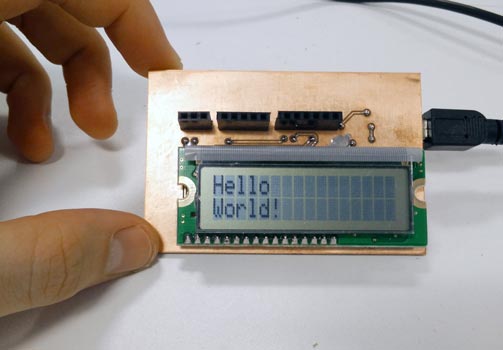
Here's the final outcome:
What Does It Do?
I often find myself working on projects where I want to display variables on a screen while I'm developing, but don't want to have to dedicate 7 pins to an LCD. I almost always have a UART, I2C or SPI bus in a project though. I also find that many character LCD displays have a set working voltage (e.g. 5V or 3.3V), but my projects tend to have variable voltage supplies depending on what I'm making.
With that in mind, I wanted my board for this week to have the following functionality:
- Allow writing data to a character LCD display using either UART, SPI or I2C
- Allow communication from 1.8V to 5.5V
- Allow display of standard variable types (e.g. int, float etc) when only their raw bits are sent to the board.
That last requirement is my way of getting rid of bloated printf() functionality from boards I'm working on. Instead, I can just send the variable directly across the bus and have the display board do the string conversion.
Designing The Board
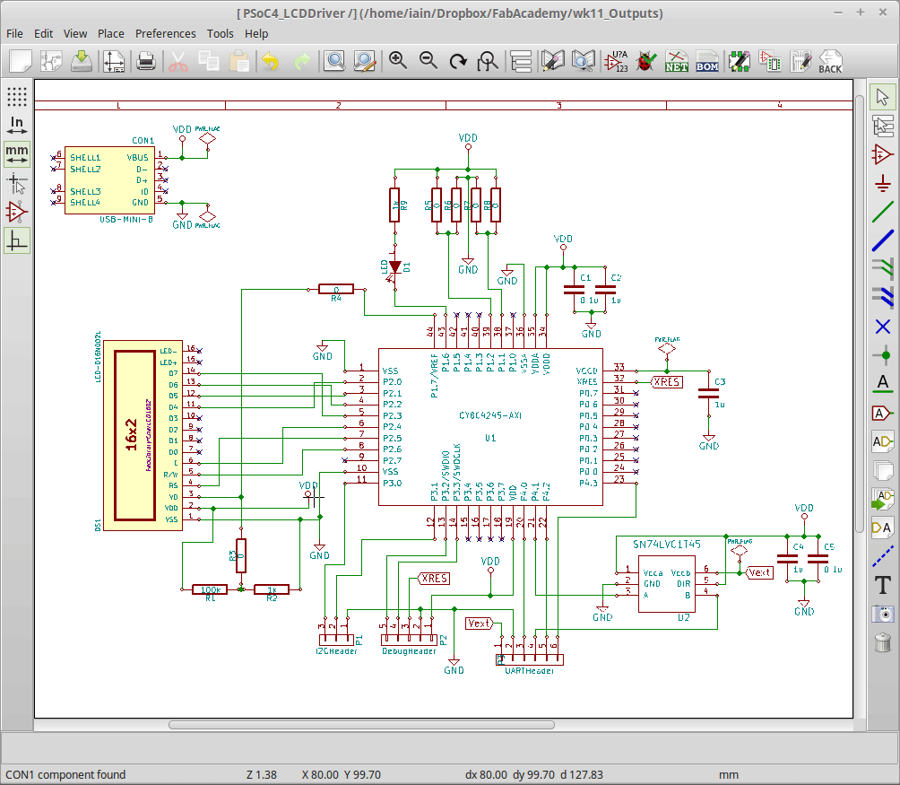
Here's the schematic for the board:
A couple of parts are worth talking about:
-
Designed to run off USB power directly at 5V
-
There are two ways to control the contrast of the display:
- Add the 0Ω resistor (or solder jumper) R3 to use the voltage divider consisting of R1 and R2 to set the contrast. The 100kΩ and 1kΩ values were copied from Neil's LCD board.
- Add the 0Ω resistor R4 to connect P1.7 of the PSoC to the contrast pin of the LCD. The idea was to use PWM to control the contrast in software. I had no idea if this would work, hence the jumper connections.
-
The PSoC 4 can be set to use LVTTL levels for inputs. That means that an input as low as 2V gets counted as logic HIGH. That's pretty nifty for getting the communication buses to work at a range of voltage levels, as it means I only have to shift the voltage of signals generated by the PSoC 4 (assuming that the source board Vdd is not higher than the display board running at Vusb). Each protocol needs voltage translation handled slightly differently:
- I2C uses pull-up resistors to hold the lines high. That means as long as the pull-ups are tied to the source board voltage, the display board can be an I2C slave with no extra components necessary. I2C gets a dedicated header on the display board.
- SPI Slave/UART only need voltage translation on MISO/Tx. I'm using the same SN74LVC1T45 chip as I used on the PSoC Breakout Board to do the translation. SPI and UART share a header.
-
I broke out P1.1 and P1.2 to be used as jumpers for configuring settings. The original intent was to use them to configure the I2C address of the board but I might have to use one of them to select if the board is in UART or SPI mode. In hindsight I should have added a switch for that...
Board Layout
I started out trying to do a single layer design but it was a nightmare. As luck would have it, we had a delivery of some double sided FR1 that was almost exactly the size I wanted the final board to be. Instead of driving myself insane trying to do a single layer board, I took the opportunity to try and do a double sided PCB on the Denford.
Here's the final layout. Note that this is the fixed version. More on that later...
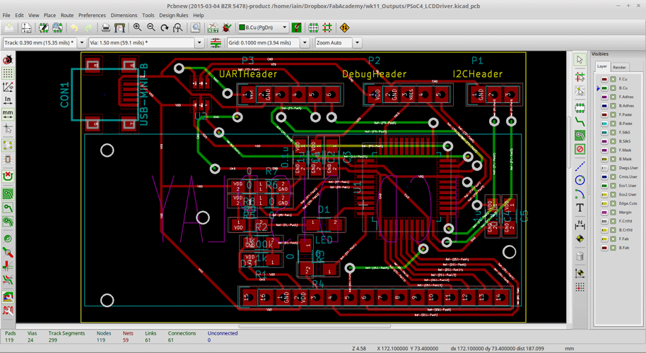
The big vias on the left hand side of the board are registration markers I added to help me flip the board to cut on both sides.
Making The Board
I exported my Gerbers from KiCAD into the Denford software. As before, I had to hand edit the drill file (I really should get round to writing a script for that...). I also added some fake tool changes into the final GCode so that I could give the motor a rest. I started out by milling and drilling the top of the board. Milling used a 1/64th bit and drill holes used a 1mm bit.
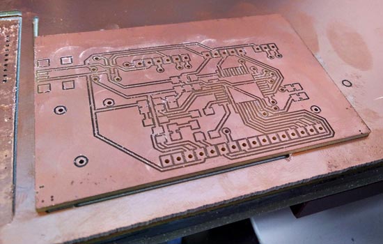
To get a good registration for the second side I mirrored the bottom Gerber in the Denford software and then extracted the GCode for the drill holes for the registration vias into a separate job. I ran the registration hole job with just the sacrificial layer of FR1 (without changing the origin from the first job) and then used some pins to align the flipped board.
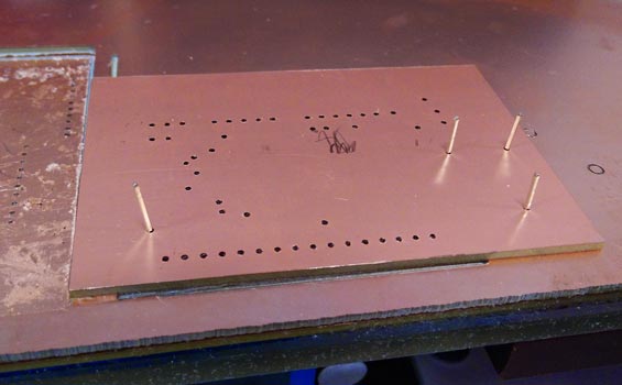
The 1mm drill holes had a bit of slop with the pins I used but the alignment between the layers ended up being pretty good.
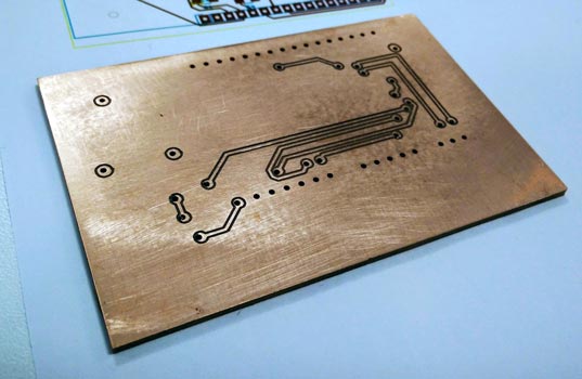
It's by no means perfect (you can see that some of the holes aren't completely surrounded by copper) but certainly functional.
Feeling like things were going a little too well, equilibrium was soon restored when I started soldering the board.
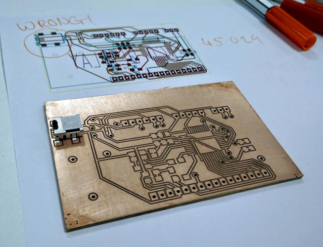
Yup, I had managed to put the USB header on so that it faced into the board. D'oh! As you can see in the picture, I had even printed out my circuit before hand so that I could check the footprint I had made for the PSoC 4 chip. Lesson learnt? Print out your layout and place ALL the parts on it to make sure everything is sensible!
Instead of cutting a new board, I flipped the header, cut the now reversed power traces and used my god-like soldering abilities to attach some jumper wires.
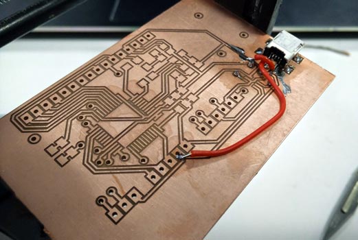
After checking the fix with a DMM, I soldered the rest of the components. Since the vias between layers obviously aren't plated, I just soldered some pins in them to make the connections.
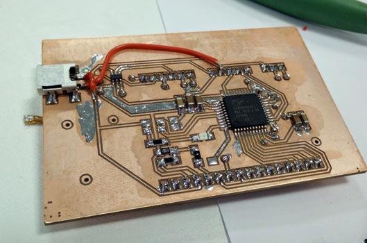
It was now time to cross everything and try to program the board...
Programming The Board
Since I had used a blank PSoC 4 chip, it didn't have a bootloader. I had two options for programming:
- Use a CY8CKIT-049 42xx to program another PSoC4.
- Use the KitProg from my CY8CKIT-042-BLE Bluetooth Low Energy (BLE) Pioneer Kit, which has the added benefit of having debug capabilities (hallelujah!).
I threw together a quick program in PSoC Creator to flash the LED I had added to the board, because that's the universally accepted method of proving a new embedded design workflow. I hooked the board up to the programming pins on the Pioneer kit, said a quick prayer and...
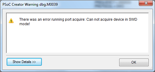
#$@&%*! (AKA Debug Time)
My first thought was that the programmer on the Pioneer BLE kit was locked to only work with PSoC 4 BLE chips, but I connected it to one of the CY8CKIT-049 4200 prototyping kits and had an LED blinking in no time. Hmmm...better check the supply voltages next.
BINGO!
It turns out that my god like soldering was slightly more human after all. In the process of soldering the jumper wires I had managed to rip up the trace going to the via in the top left of the board (the one that takes GND to the chip). A quick solder rework later and I had a custom PSoC 4 board with a flashing LED that I could program AND DEBUG!
Hard bit over it was time to get the LCD running.
Hello World!
I added the CharLCD component to my design (essentially adding a nice library to my program), specified the port the LCD was on and programmed the board.
Nothing. Again.
I was a little suspicious of the 100kΩ and 1kΩ resistor divider Neil had used (the datasheet for the display stated a variable resister of around 10kΩ). To check, I wired a 10K potentiometer on a breadboard, connected it to Vo of the LCD and tried again.
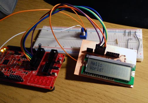
SUCCESS!! I went back and checked my board and it turns out I had soldered the 100kΩ and 1kΩ resistors in the wrong places (essentially tying the contrast to almost 5V and therefore not showing anything on the screen). I took the chance to try connecting the contrast to the PSoC PWM and found that I actually got the best contrast when I just tied the Vo pin of the LCD to ground. Over engineering FTW.
So there we have it, a basic proof of concept. I didn't have time to implement the UART/SPI/I2C component of the design yet, but I can probably count that as part of Networking week.

Get The Files
I'll turn this into a GitHub if it becomes something useful people might actually want to use.
For now though:
Comments
comments powered by Disqus