Fab Lab Barcelona SuperNode /Fab Lab Sevilla /Jose Perez de Lama
hello.arduino.168 example and tutorial / Part.04
[developed april/may 2014]
7./ Detailed fabrication process description
Here we go!
(7.1) Board preparation and milling
The orthodox Fab Academy way to prepare the milling paths and then mill the PCB is using the CAD-CAM tool Fab Modules and directly through it managing the Roland Modela MDX-20. The work flow would be: .cad or .png to paths and paths to fab send). Instrutions for this workflow can be found here:
Fab Modules installation instructions: http://kokompe.cba.mit.edu/
Milling: http://fab.cba.mit.edu/content/processes/PCB/modela.html
However, we still are milling with a Roland I_Modela and haven't connected it yet to Fab Modules. Besides that, the files generated with Fab Modules even if playing with the parameters, seem to be too optimistic for the precission that can be achieved with our I-Modela, and in my experience it is good to modify the files a bit to make sure the milling comes out correctly.
My workflow, then, is as follows.
[1] Open the make_png_dxf Fab Modules module and load the traces.png file. Note down the board size (you might want to use these dimensions to double check unit conversions throughout the process).
With Fab Modules i generate a path dxf path file. My choice is to put a very small mill diameter (0.01 mm), offset vale = 1, and no error pixels = 0, so that i get a dxf path file which is quite approximate to the actual design, that i can use in the next step in a CAD software to generate the actual milling paths. With my installation Fab Modules automatically saves the dxf file in my home folder.

[2] Then i i take the dxf file generated with Fab Modules and open it in a CAD application, in my case i am using Rhinoceros. When importing the files you have to pay attention to units. The Fab Modules file is in inches. With the I-Modela you will eventually be working with mm. My choice in Rhinoceros is workig in mm. To make sure the size is correct i double check with the board size that i noted down in Fab Modules (in this case dx = 45.466 mm; dy = 29.210 mm).
After having milled a couple dozen boards with the I-Modela i have generated my own design rules to redraw the milling paths around paths and tracks, and also for track separation, assuming i will be milling with a (rather) new 1/64'' end mill. My default values are: offset = 0.26 mm, and separattion between track axis 1mm. In some PCB spots this default values cannot be satisfied - signficantly between the microcontroller pin pads. Between the microcontroller pads i am drawing a single line (path), so that the size of the pads is not unnecessarily reduced. In other critical spots, such as the areas in between the ISP connector pads, i try to keep the separations as close to my default values as possible. In this case, and in order to make the milling process, and later the stuffing process, easier, and as a consequence of applying my design rules, i made the board a bit larger that the original. Right now i am going for a single offset, which seems to be enough. Of course it would be desirable to mill away all non necessary copper, but this process takes quite a lot of time and end-mill life.
(*) These are the values that i actually used for the second board (Fabkit) presented further down. The hello.arduino.168 board that i am showing here i milled with two offsets which laying quite close ended up being redundant. Only between the microcontroller pads i opted for a single offset, that later on, in "my design rules", commented above, i simplified even more to a single milling trajectory.
(Because i am a bit obsessive,) i have generated a graphic (Rhinoceros) data base with the various component pads that i use to make sure the files generated with Fab Modules are good enough, and they of course are, - even if sometimes the microcontoller pads are a bit smaller than they could be. The pad sizes and topolgy you can get from the respective data sheets. components_3dm
In this phase i add a name to the board which is always useful to remember later on what they are. I recommend to join all lines before exporting the file for milling. This makes the milling process smoother. For me it is useful to include the board perimeter in the milling file to make it easier to calculate how to position it in the milling surface.
This is a Rhinoceros screenshot of the milling file. The actual files can be dowloaded with links at the end of this section.

Image of the hello.arduino.168 milling path.
[3] Eventually i export the file as an .ai format, that can be imported by the I_Modela software.
Here you can download my milling hello.arduino milling file in Rhinoceros and .ai format.
hello_arduino_3dm | hello_arduino_ai
(7.2) Milling the board
Even if we are spreaking of "digital fabrication" as far as i am concerned, milling PCBs in an I_Modela is as much a craft as an "art". What i mean by this, is that it sin't such a straight forward process as one first imagines.
To begin with, as you want to use an 1/64'' inch (0.397 mm) end mill (flat end) which comes with an 1/8'' (3.175 mm) shaft diameter, you need a special collet (adaptor) to fix it to the machine. This you need to get from Roland, and didn't use to be an easy task, at least in Spain. The end mills are also difficult to find, and expensive, too, and they don't have a long life (three or four boards...). We have been using mills provided by the Fab Lab Network [see pictures and models].
[1] Physical part of the process
General instructions are well described here: http://fab.cba.mit.edu/content/processes/PCB/modela.html.
First of all fix the board to the milling bed (it should be protected with a "martyr" board) with double sided tape. Four pieces next tp the corners, not too small, should be enough.
Once the board is taped, calibrating the board planarity is one of the key steps to achieve a succesful result... Compared to the precision we need to work (around 0.01 mm in the z-axis) the boards are never planar enough. My own way is to "scan" a grid of points in the area i am planning to mill within the board, in the z -axis using I-Controller (the I_Modela software used to move the mill around and set the milling coordinates), and a thin piece of paper, and find out the actual z variations [see image below]. Then i choose the point with the lowest z value and set there the user coordinate z = 0.00. X and y users coordinate zeros can be set independently and i try to pay attention setting them so that the size of the PCB to mill does fit in the board (we are using 2 * 5 inches boards; 50.8 mm * 76.2 mm).
This is a rather boring part of the process, and it usually takes me around 20 minutes, but it is essential - in my experience - if yoy want the work to come out well.

Tracking the z-axis calibration process and milling results
[2] Setting the CAM parameters
Milling parameters are set with I-Creator. My recommendations here are:
Place the lower-left corner of the board in the 0,0 position of the I-Creator interface. This is important, because you might need to re-mill parts of the board later on, and if you want to mill the perimeter of the board with the Modela using a larger end mill (1/32'').
My milling parameters: mode, engraving; diameter 0.4 mm (not relevant as it will mill on top of the lines); speed 30/40 mm/s and 20/30 mm/s for vertical movement (rather slow but i believe this is a good choice); 0.01 mm for layer depth (again this seems to be the default value the machine works whatever data you input).
[3] Milling
Once you have this set out you can press "Cut" and the machine starts milling.
Even if you were careful setting up the end mill in the z axis watch the machine working in the initial part of the process to make sure it is actually cutting the copper away. If for some reason it is not, stop it and reset the z coordinates and mill position and fix to the collet again.
While milling keep an eye on the I-Controller interface, and manually stop the milling process when it has done the whole process to a 0.01 mm depth. The board should be ready with one layer.
As the machine doesn't do it automatically, i like to keep track of the time taken by the machine, so i try to write down starting and ending time, - as well as the milling parameters thay i have used. This is useful for future works.
(7.2.1) Debugging the milling process
Once the first milling round is done, don't take away the baord from the machine bed before observing it carefully with a good light and magnifier lens.
It often happens, that there are some parts that have not been milled ok. Identify the exact areas / lines, go back to the CAD milling path file and make a new files with only those that have not been milled.
Load the new file, paying careful attention to set it exactly in the same position in the I-Creator interface (lower left corner in 0,0), of course keeping the x and y user coordinates in the machine. Reset the z-axis 0.0 coordinate and end-mill position in the areas that have not been milled. Try to make it in the area which looks lower. Check that the milling parameters in I-Creator are those that you need, and press "Cut" again.
This process doesn't look too scientific... I write it here, because it is when things don't work as they should when beginners get stacked. I hope you don't need to do this, but just in case. Using this procedure we have lately improved enormously in our PCB production...


Then, once you believe the traces have been correctly milled, you can untape the board from the machine. I like to look at it against the light and make sure every path looks good. The board below looks quite good to me, especially the microcontroller pads which are quite regular and wide enough to solder with ease. You probably want to double check for continuity with a multimeter if some paths were looking flimsy. You can also work on the board with a very fine knife to remove small rests or clean up any path if needed. I think i did in this case in the lower right hand corner.

Scrub the board with a conventional dish washer, and apply lacquer so that it doesn't get rust, which is bad for soldering.
Cut the perimeter. Yo can do it in several ways, the orthodox Fab Academy one making it with the Modela using a wider 1/32'' end mill. In this case we cut it with the laser cutter, as mentioned above, placing the board upside down, and finishing it with a manual cutter and abrasive file.
(7.3) Components soldering / stuffing
Here comes the part of the process that has been more difficult for me to master. Again it is a balanced mix of art and craft.
The equipment needed is listed above. I definitely need a quiet moment to do this. This is not a soldering tutorial, of course but i will put down some tips that have been helpful for me.
[1] Have an image of the board with components description in front of you - in the computer screen or paper-printed.
[2] Use magnifier lamp, vise and third hand to fix the board, and components such as connectors, when possible, and tweezers to place the components.
[2] Follow the soldering order suggested by Fabio:
_ Microcontroller
_ LED
_ All other parts except connectors
_ Connectors
[3] Use plenty of flux, especially for the microcontroller pins (this makes a huge difference indeed).
[4] Prestain the pads (unorthodox way but it does make it much easier).
[5] Place with a lot of patience and care the microcontroller in its place, and solder one of its corners pins right. Once you achieve this everything gets easier. Keep applying flux to the pins when soldering. If the micro moves a bit when soldering don't panic... The pins can take a small physical tweaking that you can achieve with a fine kife - or course that is not the optimum scenario, but it has worked for me sometime.
[6] In this example, we are not soldering the 8MHz resonator. However, prestain the pads so that it is easier to solder it in the future.
[6] Soldering the LED you have to pay attention to polarity. Check the PCB image to see which sides correspond to positive and negative ends. Not so easy to identify these ends in the LED though. The negative side has a dark line in the transveral direction that you have to look for with a magnifier. Check the data sheet if needed.
[7] Once you have soldered the microcontroller, all other components look huge in comparison! So everything becomes much easier, even if capacitors can be a bit rebellious.
[8] If something goes wrong with the soldering, relax, and be patient desoldering - you may easily take away pads or tracks if you are too impulsive. My choice for desoldering is braid, and taking it very easy, repeating the process several times until it is done.

Checking that the microcontroller pins can be correctly placed

Prestaining microcontroller pads

Soldered microcontroller... Not the cleanest piece of work. Next time will hopefully be better... (The jigsawed aspect of the milling work is an effect of image compression or who knows what. The real thing is perfectly straight)

Microcontroller, LED, resistors and capacitors stuffed
Now, i forgot to cut the board, and i realized i needed to do it, at least in the part of the FTDI connector... That was a little mistake... I cut the side that i needed to cut with a laser cutter, as mentioned before.

Eventually here is the fully stuffed hello arduino with switch and connectors. Cutting and sanding the board in the middle of the process made it quite dirty...
(7.3.1) Solder testing and debugging
This part, again, is essential, at least for beginners.
Study carefully the connections for each microcontroller pin and use a multimeter to check continuity with connector pins or whatever they are connected to. My recommendation is to make it in order, from 1 to 32, writing down in a diagram the results. The lacquer applied at the end of the milling process can act as isolator, so you often have to go for the sides or edges of the tracks with your multimeter to get continuity. After testing the microcontoller pins test the other components. My score lately amounts to a mean of three to four solder points to fix after the first round.
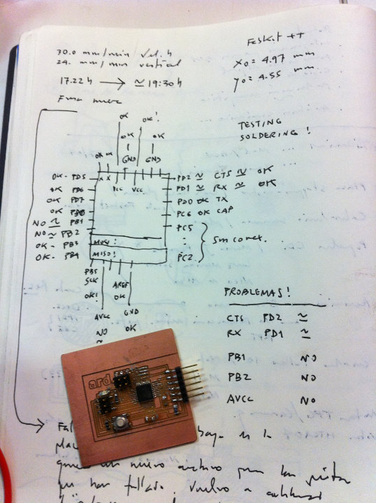
Image: Tracking the solder testing process
Install all your vise and parafernalia again and resolder where needed. Don't forget to use flux for resoldering.
Test again with the multimeter and if everything is working that ir should be, move on to the next section.
(7.3) Bootloading firmware and uploading your first Arduino sketch (program)
Here we go.Bootloading the firmware for the hello.arduino.168 board is not difficult, but of course you have to pay close attention to the process.
Connections
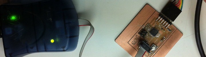
First you have to connect the AVRISP mk II to the board ISP port. Check the board png to identfy it. In order to know how to place the connector check the MISO, VCC, SCK, MOSI, RST, GND distribution on both connectors. The red line in the AVRISP connector corresponds to port number 1 - MISO. (See diagram and pictures below).

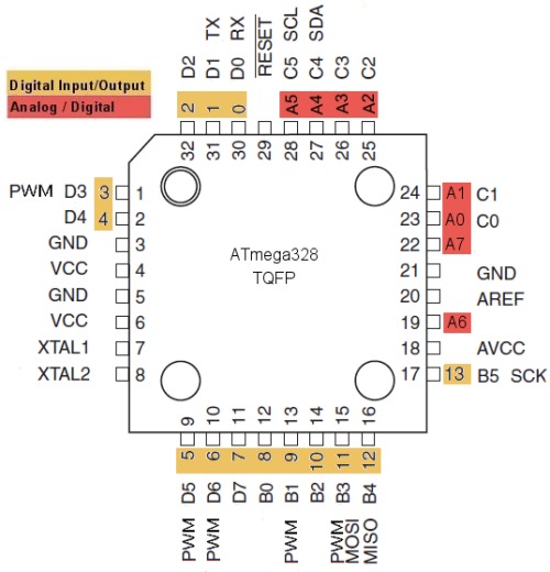
You may also want to consider the ATmega 168 pin layout, to understand how the connections should be made and especially to be able to program the board once it is bootloaded:

Nice image/diagram by pighixxx.com
This second image contains less info but might be easier to read.
When first connecting the AVRISP mkII, to the board ISP port, and on the other end, to the computer USB port a green LED should shine in the ISP, meaning the connection is ok. Otherwise something is wrong and you would have to test what it might be:
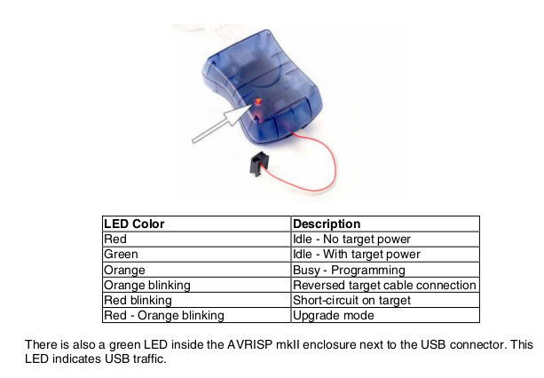
Source: AVRISP mkII User Guide
Then you have to connect the FTDI port with an FTDI cable. I believe it should be a 5V cable. In my cable you can check the voltage written in the USB connector. To know how to connect it check the board layout for the GND pins and put on this side the black (GND) cable of the FTDI connector.


Here you can see the connections: (1) AVRISP to board ISP port; (2) AVRISP to computer USB port; (3) board FTDI port to computer USB port 2. You can see, too, the green LED on the AVRISP, meaning that the connection is ok but idle at the moment.
So, now that the system is connected comes the actual bootloading process. As metioned before, in this tutorial qe are using the Arduino IDE. Previously we should have added the board firmware for this particular version of Arduino which is not included in the default installation. In order to fo this follow the instructions in section 5.5 of this tutorial.
If everything is correctly set up the process is extremely simple. Open the Arduino IDE. By default my Ubuntu 13.10 recognizes the port where the system is connected, so i don't have to do anything about this.
In the Arduino IDE go to the Tools/Board and select the entry Fabkit/Fabduino w/ATmega168 (internal clock).
Go to Tools/Programmer and select AVRISP mkII
Go to Tools/Burn Bootloader and the firmware should start bootloading.
The LED in the AVRISP and in the hello.arduino boards should light or blink for a few seconds.
Ate the end of the process if everything went ok on the bottom of the Arduino IDE a message should prompt saying Done Burning Bootloader. You should be done with this!!!
Now you can disconnect the AVRISP and keeping the FTDI cable connected, try to upload an Arduino sktech to the board to test it is indeed working. The usual thing is to upload the blink sketch that works with the LED incorporated in the board. In the Ardunio IDE go to File/Examples/01.Basics/Blink
This opens the sketch code in the IDE main window.
Click on the Upload button (second one with arrow pointing to the right).
The LED on the Arduino will light for some seconds. After this a prompt at teh bottom will tell you the process has been succesfully completed.
The LED in the Arduino will start blinking with the rythm written in the blink sketch. Now you can start thinking what you want to do next with your new hello-arduino board!!!

This is my first hello.arduino, probably, just after uploading the blink sketch. You can (barely) see the board LED lighted, just below the ISP cable.
A video of the functioning board can be seen here: https://vimeo.com/93672687
Links
Part 01
0./ About this tutorial
1./ Description :: hello.arduino.168/328P
2./ Fab Academy reference files list and location
3./ Tutorials, info sources and URLs
Part 02
4./ Workflow & toolchain
Part 03
5./ System and software requirements & installation
6./ BOM (Bill of Materials) equipment and tools
Part 04
7./ Detailed fabrication process description
7.1/ Board preparation and milling
7.2/ Components soldering and debugging
7.3/ Bootloading firmware and uploading your first Arduino sketch (program)
Part 05
8./ Fabkit fabrication notes (files, ISP cables & connection)
jose_perezdelama @ Fab Academy 2013 final project
jose_perezdelama @ Fab Academy 2013 home page
License & credits
This work is a derivative of documentation collected in the Fab Academy classes and tutorial pages authored by Neil Gershenfeld, Anna Kaziunas/AS220 and Fab Academy collaborators and students as mentioned in the corresponding linked pages for each of the sections.
Unless otherwise stated, information in these pages is downloadable under a Creative Commons Attribution-Share A Like license; attribution for the tutorial reorganization: Jose Perez de Lama / Fab Lab Sevilla / Fab Academy 2013(14).