
WEEK 13
NETWORKING AND COMMUNICATIONS
Group assignment: Send a message between two projects.
Individual assignment: Design, build, and connect wired or wireless node(s) with network or bus addresses.
1. Group assignment
Go to the Sedicupct website
2. Individual Assignment
2.1 introduction I2C communication protocol
This week I am going to communicate my boards using the I2C communication port. So the first thing I have to know is what is the I2C communication port and protocol.
I2C is a serial communication port and protocol, it defines the data frame and physical connections to transfer bits between 2 digital devices. The port includes two communication cables, SDA and SCL. In addition, the protocol allows connecting up to 127 slave devices with these two lines and a single master device, with up to speeds of 100, 400 and 1000 kbits / s. It is also known as IIC or TWI - Two Wire Interface.
Links I2C port documentation:
The I2C protocol is one of the most used to communicate with digital sensors, since unlike the Serial port, its architecture allows to have a confirmation of the received data, within the same frame, among other advantages.
Connecting so many devices to the same bus is one of the main advantages. Furthermore, if we compare I2C with another serial protocol, such as Serial TTL, it includes more bits in its communication frame that allows more complete and detailed messages to be sent.
The messages that are sent through an I2C port include, in addition to the information byte, an address for both the register and the sensor. For the information that is sent there is always a confirmation of receipt by the device. For this reason, it is good to differentiate the different elements involved in this type of communication.
2.2 I2C communication scheme
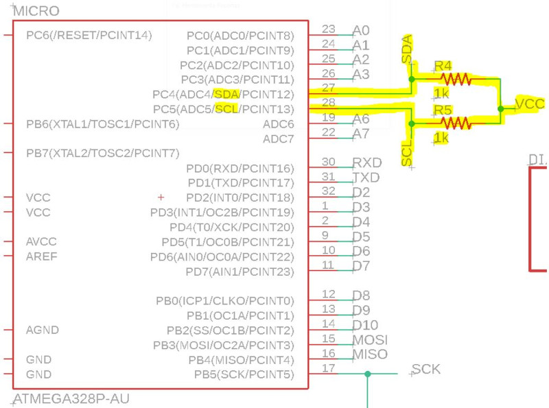
In the case of I2C, there are two basic elements, a MASTER and a SLAVE. The Figure below shows a typical connection of three devices, the bus consists of two lines called, Serial DAta - SDA and Serial CLock - SCL. That is, Serial Data and Serial Clock. In particular, two resistors are connected to the bus in a pull-up arrangement, between 2.2K and 10K. (resistors connected to positive) to ensure a high level when there are NO devices connected to the I2C BUS.
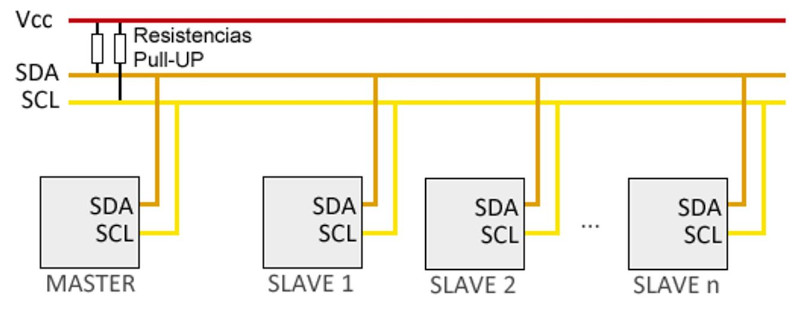
The I2C Master is in charge of controlling the clock cable, for its acronym in English called SCL - Serial CLock. In addition, it is responsible for starting and stopping communication. The serial binary information is sent only by the serial data line or cable, in English it is called SDA - Serial DAta.
The I2C Slave is usually a sensor. This element provides the information of interest to the Teacher. It can act in two ways: slave-transmitter or slave-receiver. A slave I2C device cannot generate the SCL signal.
2.3 I2C port operation
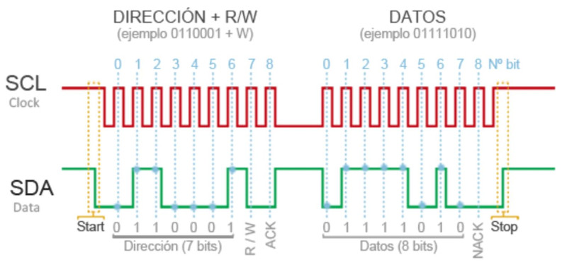
To be able to communicate with just one data cable, the I2C bus uses a wide frame (the format of the data sent).
Communication costs::
- 7 bits to the address of the slave device with which we want to communicate.
- A remaining bit indicates if we want to send or receive information.
- One validation bit
- One or more bytes is the data sent or received from the slave.
- One validation bit.
2.4 Comunicación I2C de mis boards
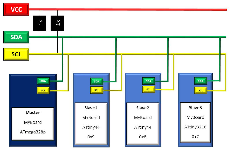
I am going to use the I2C communication protocol to communicate 4 boards, a Master (MyBoard ATmega328p) and 3 slaves (HelloBoard ATtiny44, HelloBoard ATtiny44 and Myboard ATtiny3216).
2.4.1 Master "Myboard ATMEGA328P"
The master device is MyboardATmega328p which designs week 10 "Input Devices".
This board has multiple Digital Input / Output and Analog / Digital and 3 communication protocols:
- FTDI / USART (RX / TX).
- SPI: MOSI-MISO-SCK-SS.
- I2C: SDA-SCL
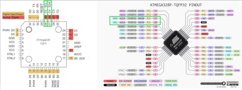
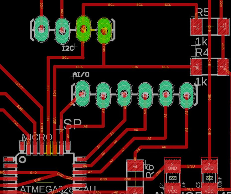
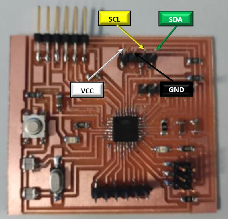
I identify in my Eagle Schematic the SDA, SCL, Vcc and GND pins. Also, I notice that they already have 1K resistors for pullup.
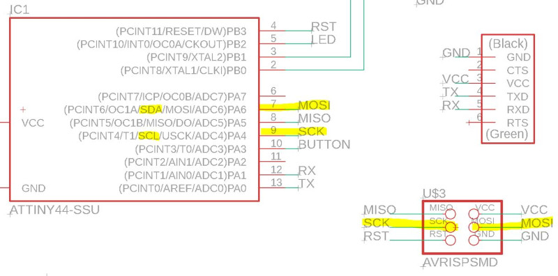
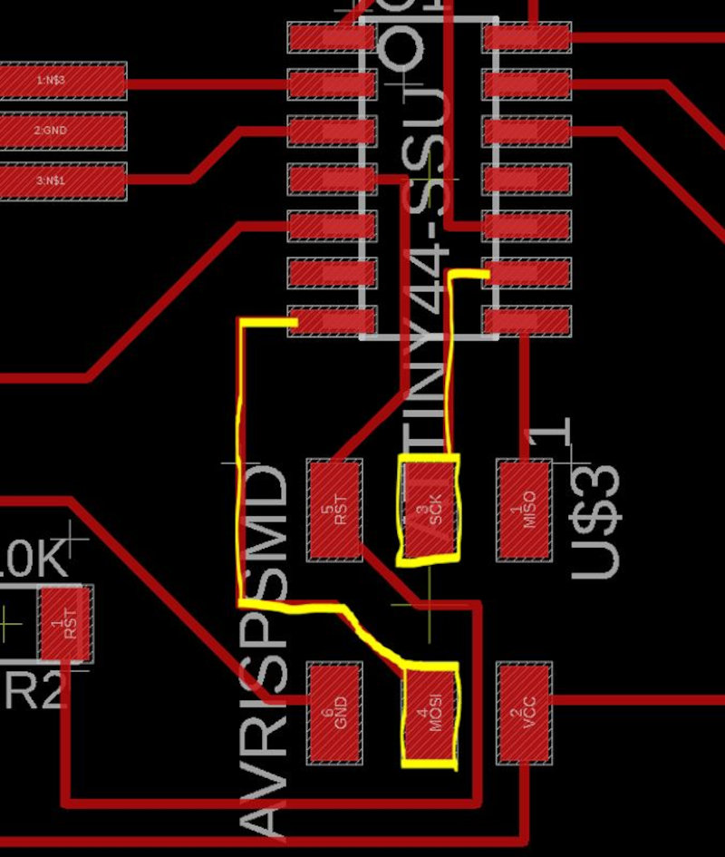
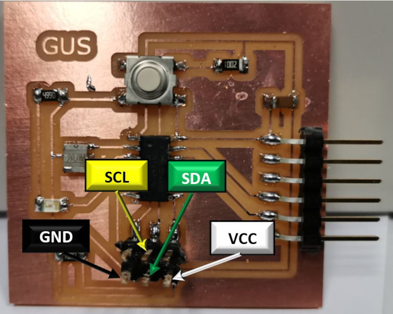
2.4.2 Slave1 HelloBoard ATtiny44 "helloftdi.attiny44"
Slave1 device is MyboardATtiny44 that I designed week 6 "Electronic Design".
This board has 3 communication protocols:
- FTDI / USART (RX / TX).
- SPI: MOSI-MISO-SCK-SS.
- I2C: SDA-SCL
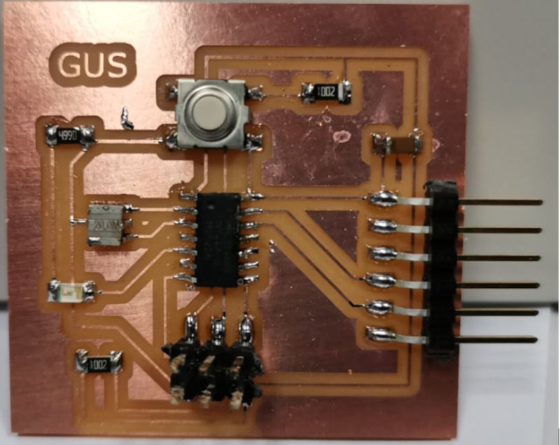
I identify in my Eagle Schematic the SDA, SCL, Vcc and GND pins. I also observe that they do not have pullup resistors.
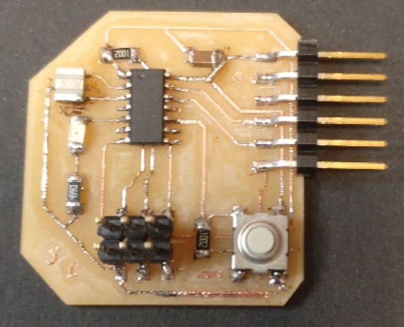
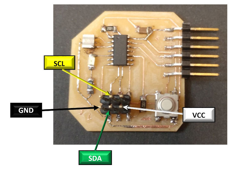
2.4.3 Slave2 Alvaro-HelloBoard ATtiny44 "helloftdi.attiny44"
For Slave2 use the Alvaro-HelloBoard ATtiny44 designed and manufactured by Alvaro Macian. This board has the pins configured the same as my HelloBoard ATtiny44.
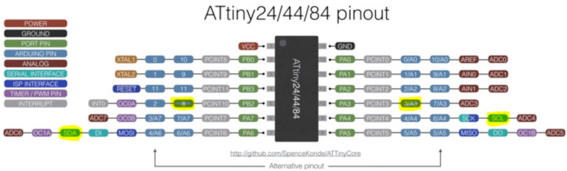
2.4.4 Slave3 MyBoard (ATtiny3216)
In previous regional reviews I was recommended to go one step further and use a microcontroller with an updated technology and better features, so I will design and use the ATtiny3216.
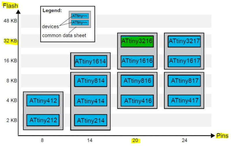
I find information about the ATtiny3216 on the SpenceKonde website.
- Pack of 20 pins.
- Internal clocks 1/4/5/8/10/16 20 MHz.
- 32768 bytes flash memory.
- 256 bytes EEPROM and 2048 bytes SRAM.
- Maximum voltage: 6V; minimum voltage -0.5 V.
- VDD: Supply voltage. GND: ground.
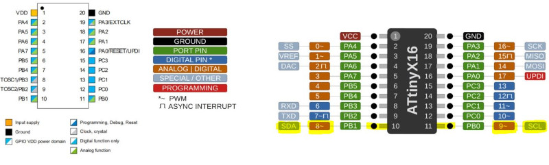
- Digital pins: Port A: PA0, PA1, PA2, PA3, PA4, PA5, PA6, PA7. Port B: PB0, PB1, PB2, PB3, PB4, PB5. Port C: PC0, PC1, PC2, PC3.
- Analog pins: Port A: PA0, PA1, PA2, PA3, PA4, PA5, PA6, PA7. Port B: PB0, PB1, PB4, PB5.
- UPDI programming pin: PA0 (physical pin number 16).
- All I / O pins can be configured with internal pull-out resistance.
Within the communications section there are different types and their pins are different. It is clear that the different communication protocols cannot all be used at the same time, because they have pins in common.
- USART - Universal and Asynchronous Synchronous Receiver and Transmitter: It has the RX (PB3 or PA2) and the TX (PB2 or PA1).
- SPI - Serial Peripheral Interface: It only has MOSI (PA1 or PC2), MISO (PA2 or PC1), SCK (PA3 or PC0), SS (PA4 or PC3).
- TWI - Two Wire Interface (I2C): Has SDA (PB1 or PA1) and SCL (PB0 or PA2).
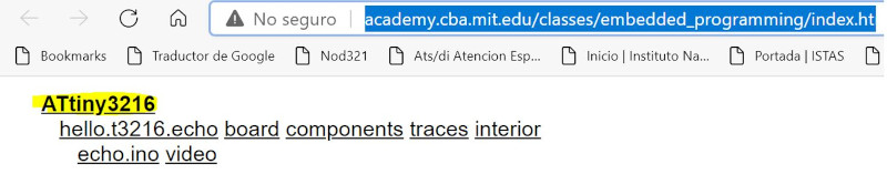
I find information about a Neil board "hello.t3216" in the week of embedded programming.
I am guided by this board for the design, but I'm going to create my board by enabling all the connection pins of the ATtiny3216.
In addition, I will be guided by what Adrian Torres did using an " ATtiny3216 board" in the week of in Input Device.
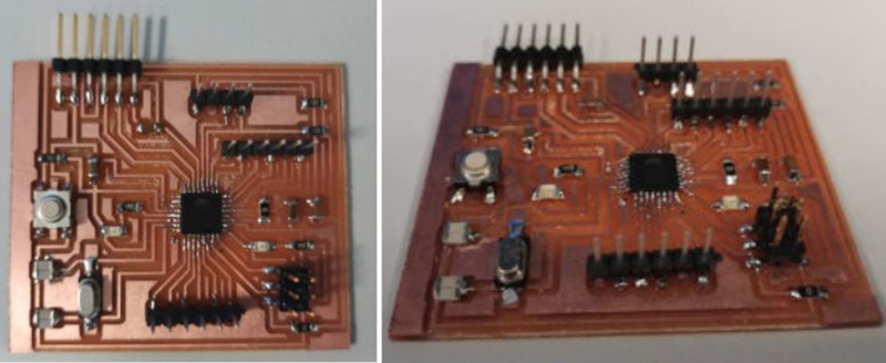
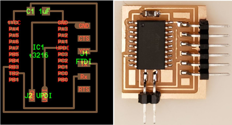
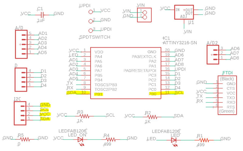
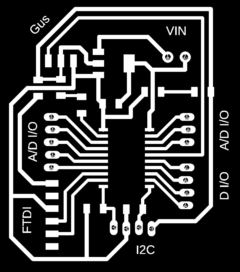
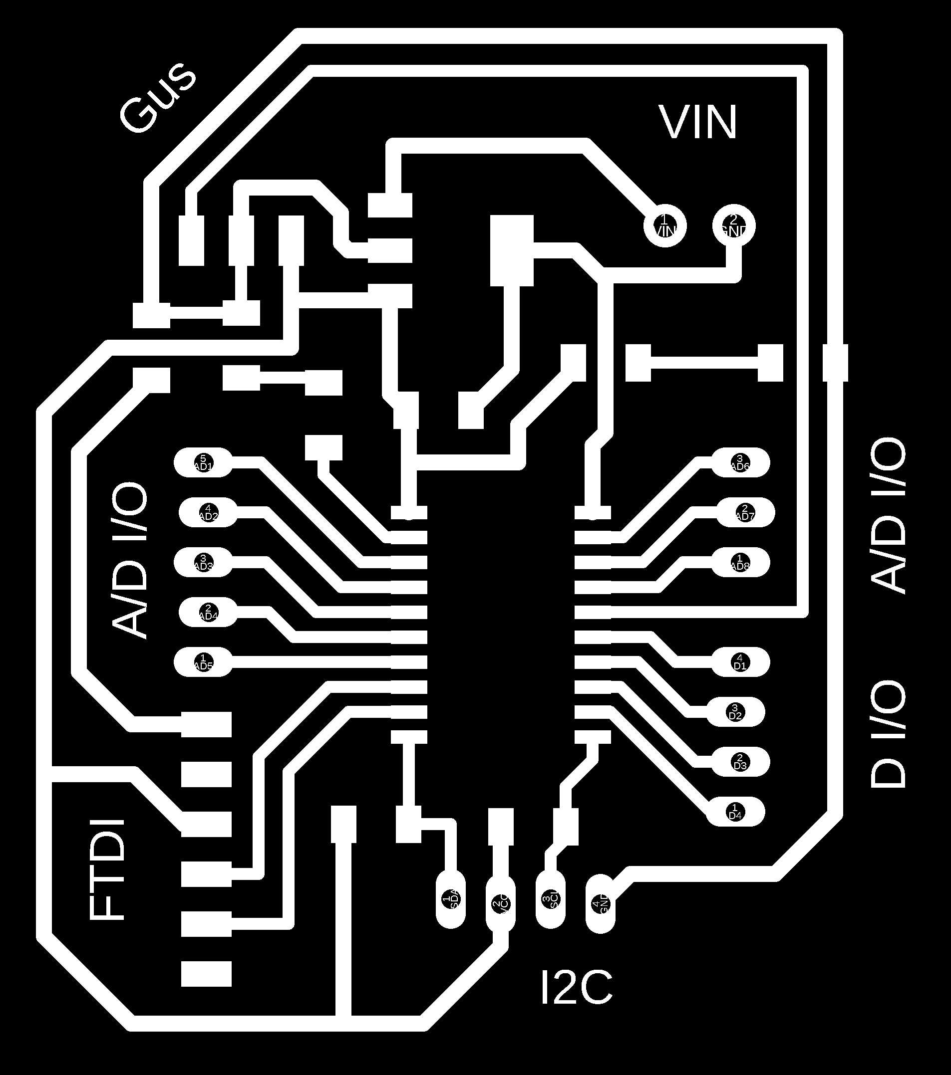
2.4.4.1 Eagle Design by MyBoardATtiny3216
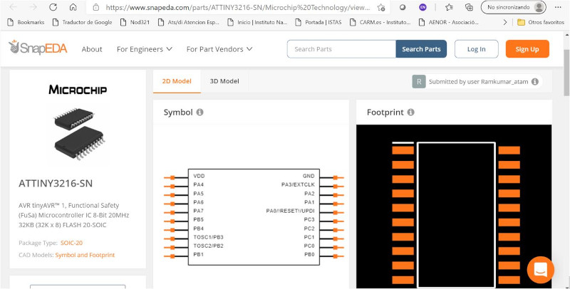
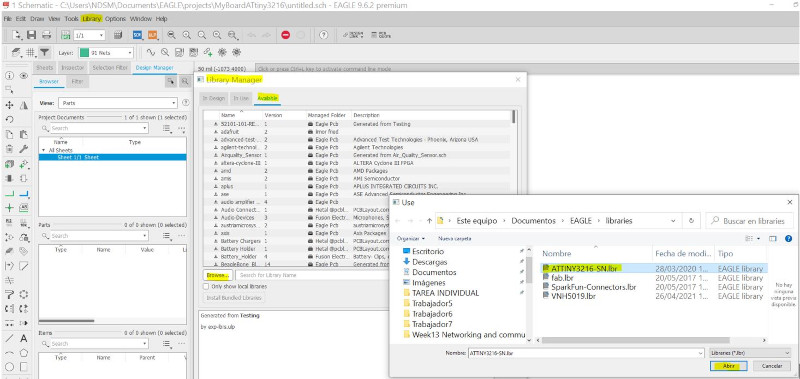
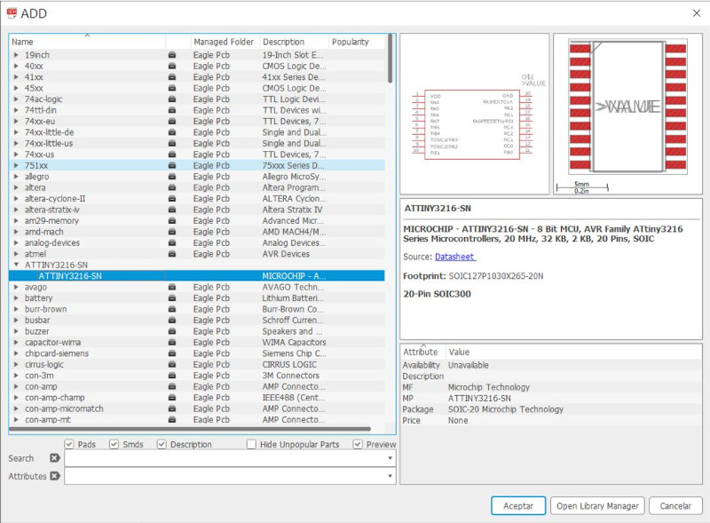
I download the "footprint of the ATtiny3216 micro" on the Snapeda page, I import the library in Eagle and add ATtiny3216.
I include in the design a regulator of (26-5V) that Adrian Torres uses on his board.
In this board I have included connections: I2C, FTDI, UPDI, Input / Output Anolog / Digital and Input / Output Digital. It has a 1x2 terminal to connect an external source up to 26Vdc.
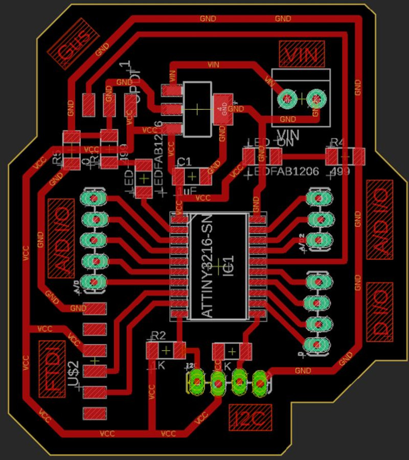
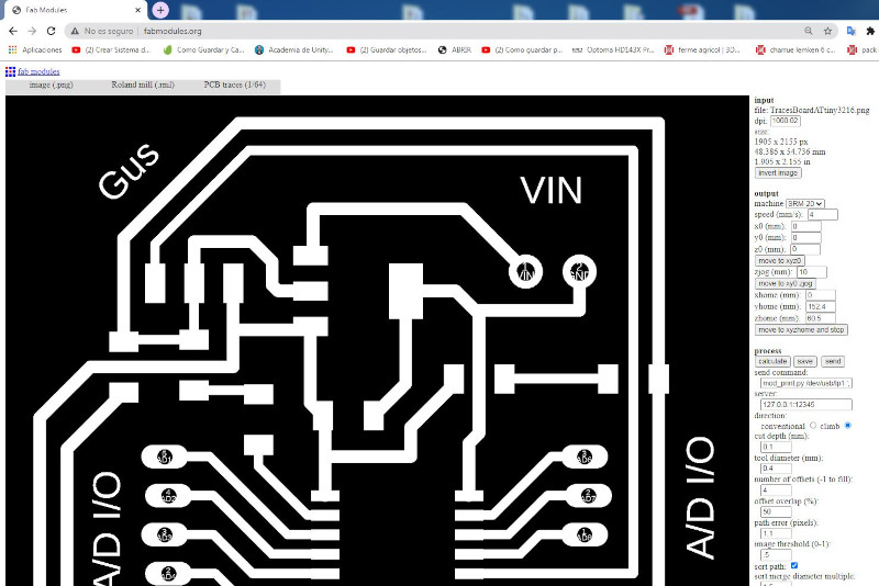
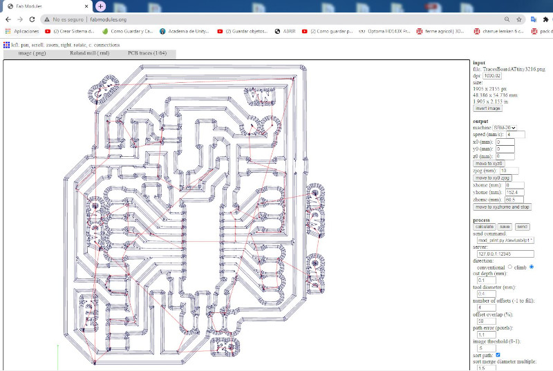
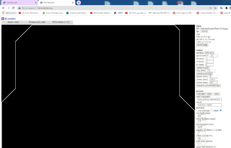
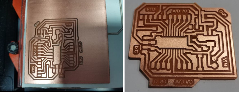
I export the .png images of the trace and the outline.

2.4.4.1 Milling
I have used the fabmodule.org with the RML-20 router to mill my board. I import the .png images of traces and outline.

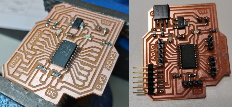
2.4.4.1 Solding
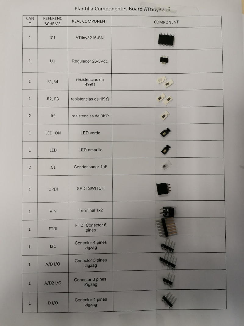
I use a template to identify the electronic components that I am going to solder.

2.5 Programming
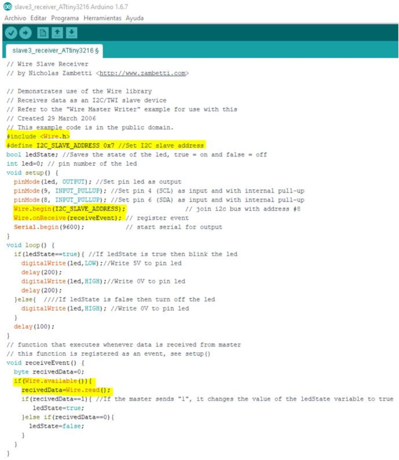
Use the Arduino IDE to program all the boards. The I2C libraries depend on the devices used, in my case the Master device is the ATmega328p and the I2C library used is Wire.h. This library is also used for the slave device3 that corresponds to the ATtiny3216. Unlike the previous ones, the slave1 and slave2 devices use an ATtiny44 that works with the TinyWireM (Master) and TinyWireS (Slave) library.
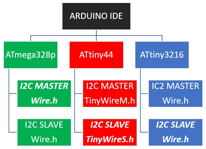
I have followed the assignements that Lola Ojado and Alvaro Macian made in which they use the Wire.h library in Arduino IDE, with the Attiny44 it gives errors because Wire.h works with TWI hardware, however ATtiny44 has USI hardware for communication.
Alvaro Macian and Lola Ojados used these libraries for I2C communication with the attinys:
- TinyWireM.h Library for the master device.
- TinyWireS.h Library for the Slave device.
2.5.1 I2C Master Programming (ATmega328p)
I use the Wire.h library to configure the Master's I2C communication. The program works with a switch button that in HIGH activates the I2C connection and starts the transmission with slave1 (0x9) sending it a byte (1) and in LOW it sends another byte (0).
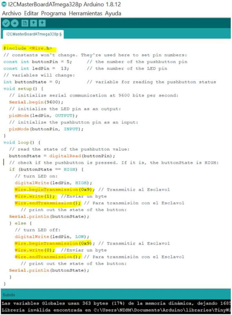
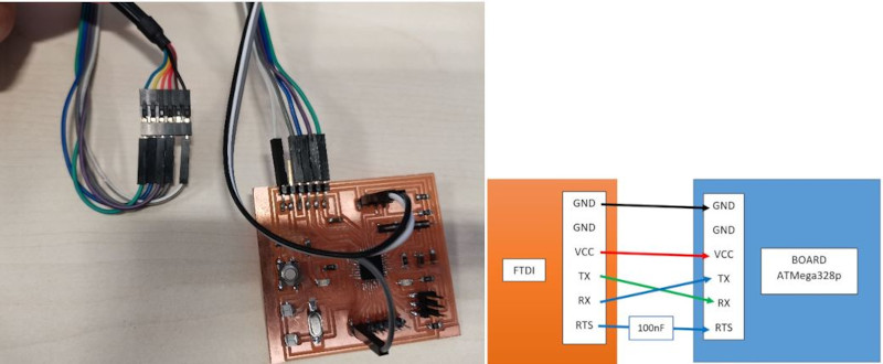
To compile and load the program I use the FTDI connector and connect it to the FTDI of the board by exchanging the TX / RX pins.
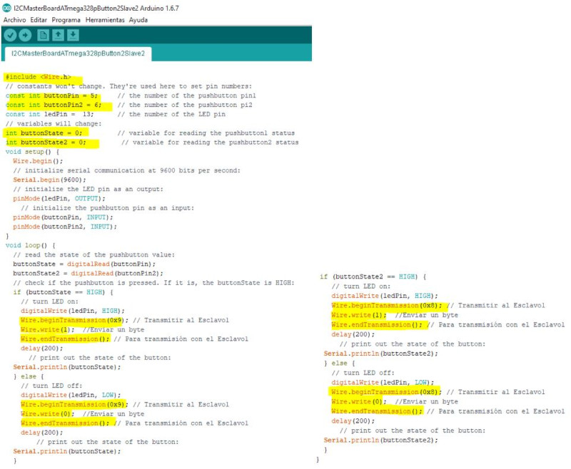
I create another program so that the master can communicate with 2 slaves, I identify the slave1 (0x9) and the slave2 (0x8). Using only one button to enable communication.
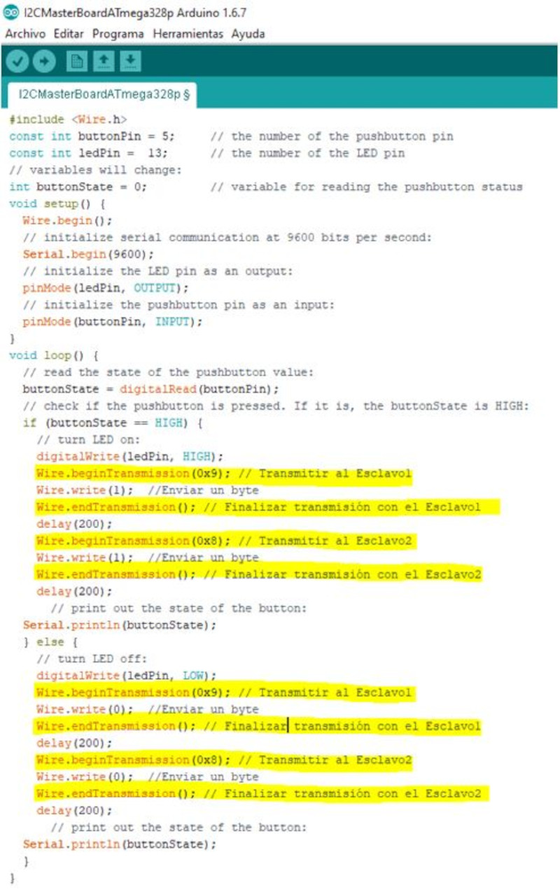
I create another program so that the master can communicate with 2 slaves, I identify the slave1 (0x9) and the slave2 (0x8). Using 2 buttons to enable communication of each slave with a different button.
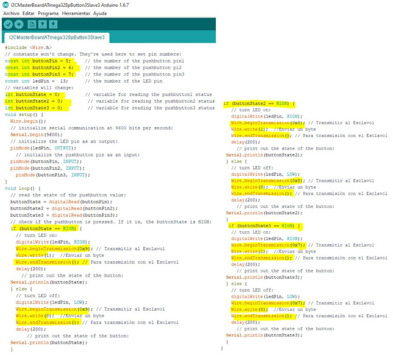
Finally, I include another program for the master to communicate with 3 slaves and with 3 buttons so that each one is enabled independently.
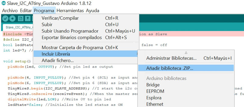
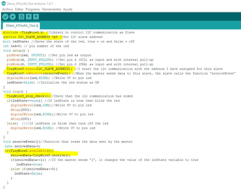
2.5.2 Slave 1 and Slave 2 I2C Programming (ATtiny44)
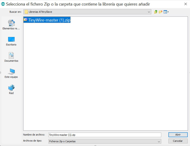
I will use the TinyWireS library.h Library for the secondary device.
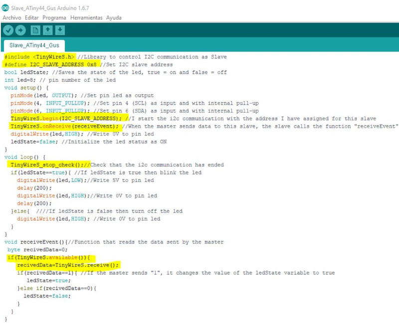
I use two ATtiny44 boards that use the same communication pins and digital output for the led, I just have to change the address of slave2 (I2C_SLAVE_ADDRESS 0x9).
To compile the program I have to connect the ATtiny45 programmer to the computer through the USB connector. The programmer connect it to my ATtiny board through the SPI connector and the ATtiny boad connect it to power through the FTDI connector.
2.5.3 Slave3 I2C Programming (ATtiny 3216)
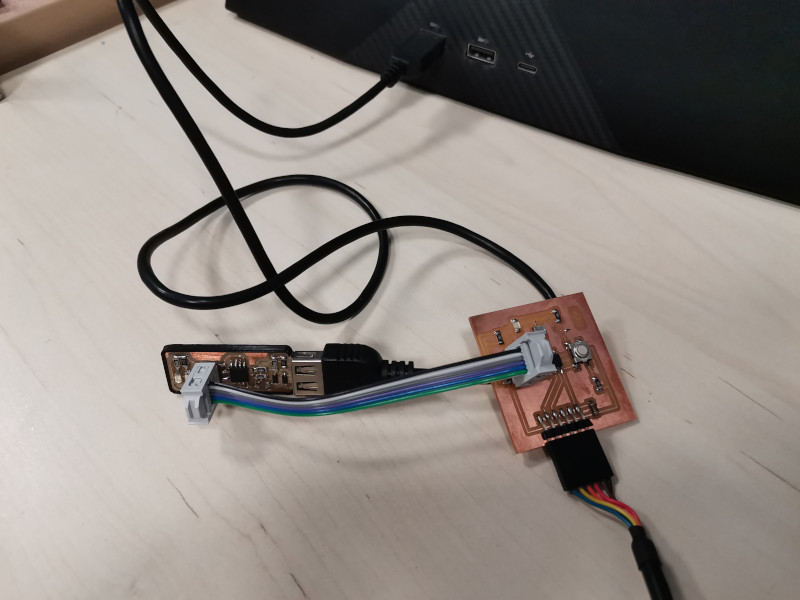
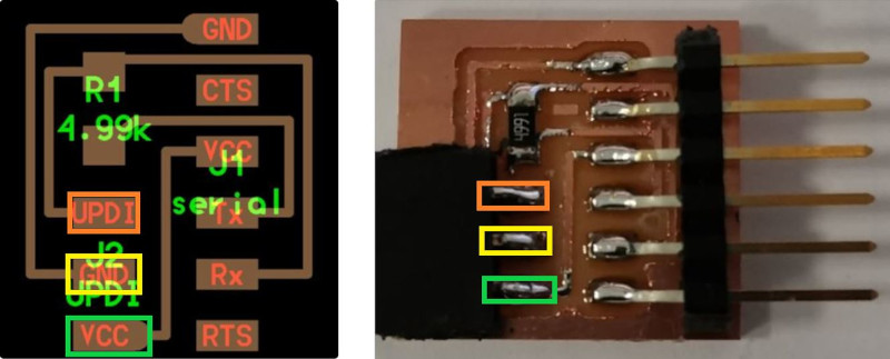
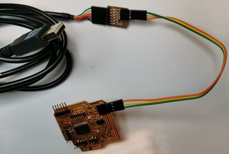
To program the ATtiny3216 I use the FTDI / UPDI connector that I manufactured in week 4 Electronic Production.
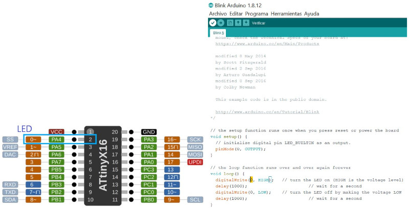
I use Arduino IDE and first load an example program "blink" and select the pinout = 0 that I use for the LED of my board, so I check that the board works correctly.
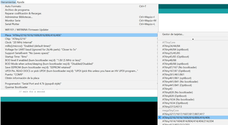
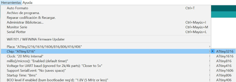
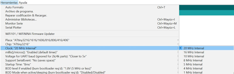
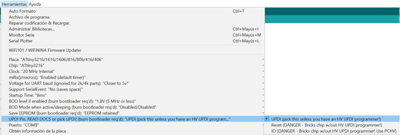
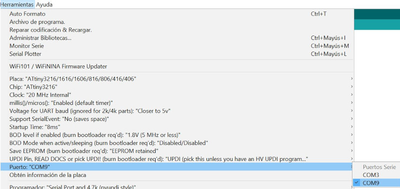
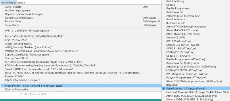
In Tools I modify the parameters to program the ATtiny3216.
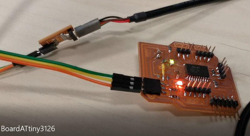
Since I have tested that the ATtiny3216 board works, next I create the program for slave I2C communication.
2.6 WIRING AND OPERATION TESTS
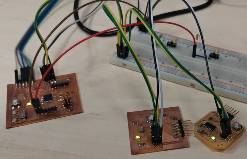
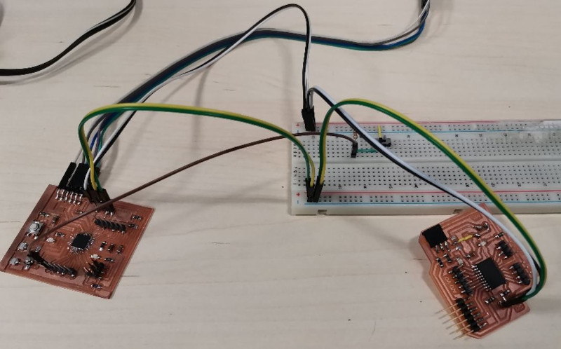
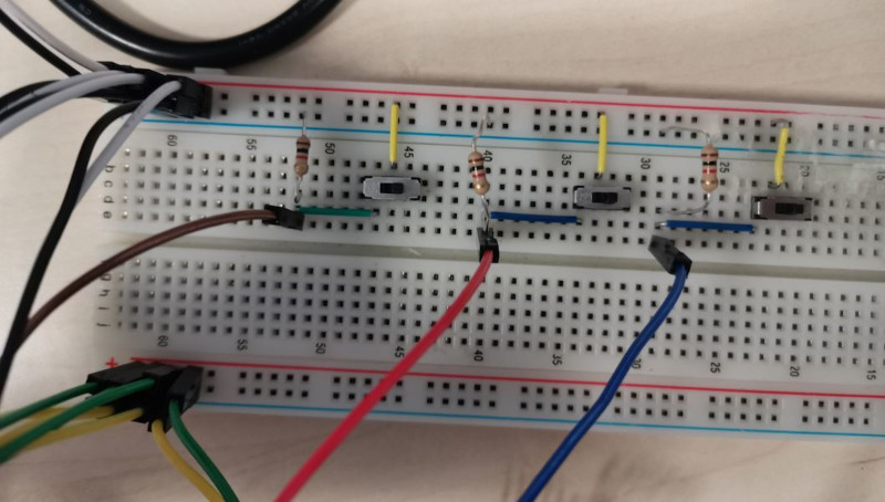
2.6.1 Master and Slave1 (ATtiny44) - 1 Switch
First I carry out the communication test between the Master and Slave1 (ATtiny44). When the breadboard switch is ON, it enables I2C communication.
- Switch OFF: Master Led off and Slave led On.
- Switch ON: Master LED on and Slave LED flashing.
2.6.2 Master and Slave1 / Slave2 - 1 Switch
I connect the Master and the two Slaves. Communication for the two Slaves is enabled by the switch. When the switch is ON, the Slave LEDs blink, informing that there is I2C communication.
- Switch OFF: Master Led off and Slave1/Slave2 led On.
- Switch ON: Master LED on and Slave1/Slave2 LED flashing.
2.6.3 Master and Slave1 / Slave2 - 2 Switch
I connect the Master and the two Slaves. The communication for the two Slaves is enabled by 2 switches that will enable the independent I2C communication of each Slave.
- Switch1 OFF: Master Led off and Slave1 led On.
- Switch1 ON: Master LED on and Slave1 LED flashing.
- Switch2 OFF: Master Led off and Slave2 led On.
- Switch2 ON: Master LED on and Slave2 LED flashing.
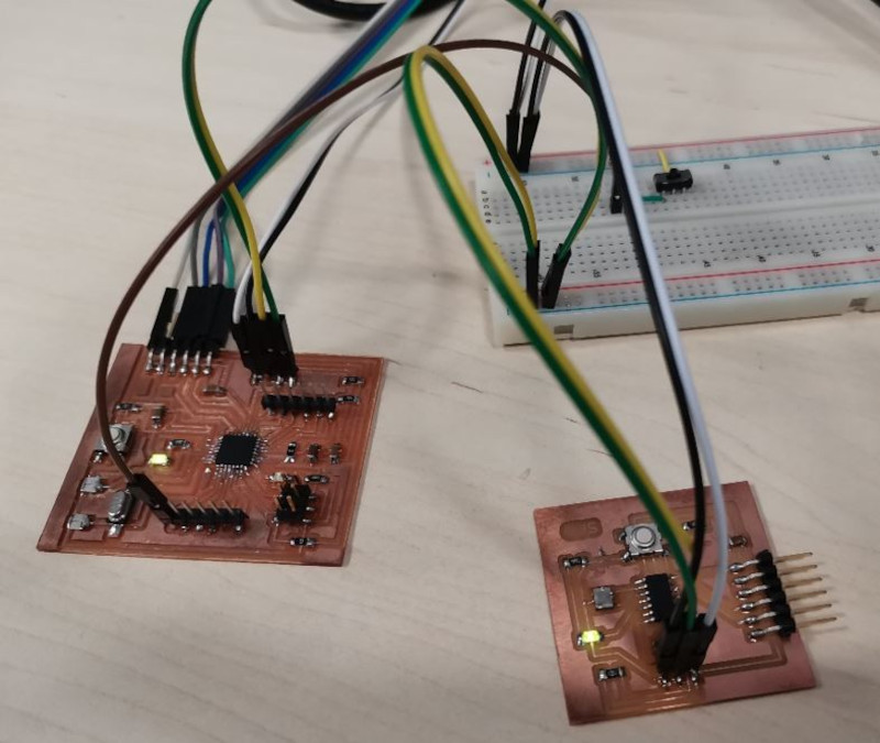
2.6.4 Master and Slave3 (ATtiny3216) - 1 Switch
I connect the Master and the Slave3. Communication for the Slave3 is enabled by the switch.
- Switch1 OFF: Master Led off and Slave3 led On.
- Switch1 ON: Master LED on and Slave3 LED flashing.
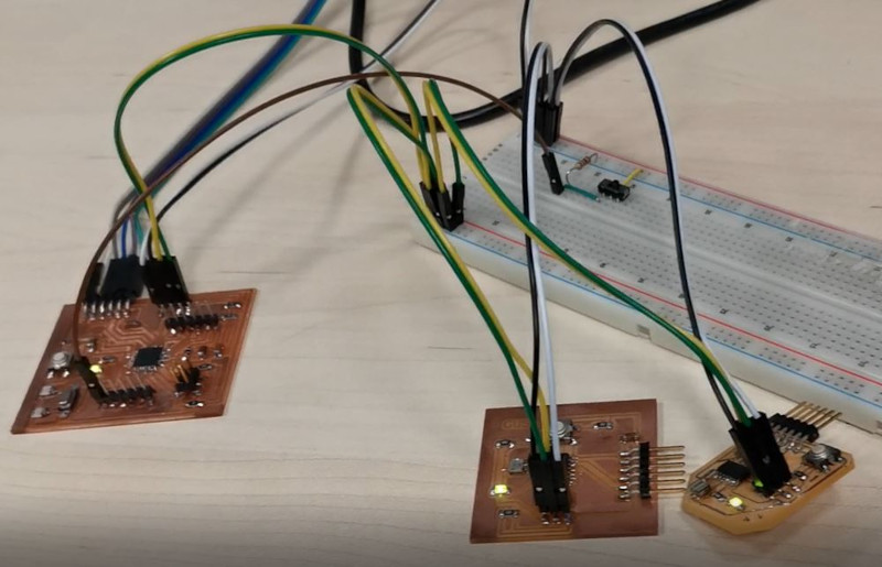
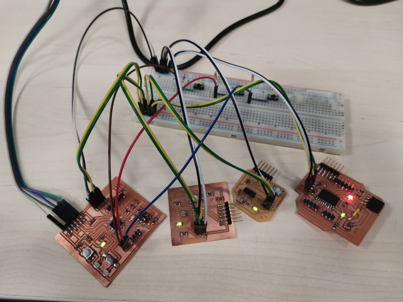
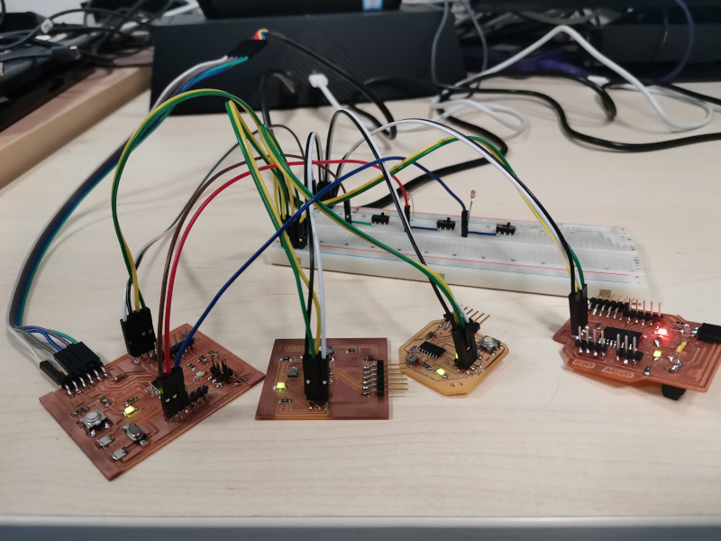
2.6.5 Master and Slave1 / Slave2 / Slave3 - 3 Switch
I connect the Master and the three Slaves. The communication for the three Slaves is enabled by three switches that will enable the independent I2C communication of each Slave.
- Switch1 OFF: Master Led off and Slave1 led On.
- Switch1 ON: Master LED on and Slave1 LED flashing.
- Switch2 OFF: Master Led off and Slave2 led On.
- Switch2 ON: Master LED on and Slave2 LED flashing.
- Switch3 OFF: Master Led off and Slave3 led On.
- Switch3 ON: Master LED on and Slave3 LED flashing.
3. Conclusions of the week
How was the week?
This week I have had more time to dedicate to the fabacademy, I have looked for information on the I2C communication protocol that I could use in the electronic boards that I have built. I was missing a board so I took the opportunity to take a step forward and build my ATtiny3216 board that I will use later in my final project. So it has been a very productive week. I have structured the communication including in each step one more electronic board until reaching 4 boards communicated by I2C.
What went wrong ?
- I have had trouble compiling the ATtiny44 because the Wire.h library in Arduino IDE works on TWI hardware and the ATtiny44 has USI hardware for communication, so I used the TinyWireS.h library for the slave device.
- When compiling the program in the Arduino IDE of the ATmega328 board, I used an FTDI connector and connected it to the FTDI pins of the board but it did not give me a compilation error. In the end I realized that it is necessary to swap the TX / RX pins.
What went well?
The design and manufacture of my ATtiny3216 board has been a success, I have not had any problems and its programming is simple. The I2C communication between all the devices works correctly, it also included some switches to select which slave the master could communicate with.