Group assignment 1
This week i couldn't join the group when doing the assignment, but i got the chance to do it again on Tuesday's class on electronic components and arduino. While I understand it was better to do it with our own circuits, the use of the multimeter really is the same on one case or the other.
So during the session, in which we learned about the role of resistances, capacitors, buttons and transistors with the comfort of the arduino environment, David Prieto and i used the multimeter to measure for continuity, voltage and current on different parts of the circuits we were assembling.


Group assignment 2
It is a yearly tradition at FabLab Barcelona, to go up the mountains to visit the Green Lab at Valldaura around February-March to do a calçotada.
This year's event was scheduled for March 6th, so a big group from FabLab Barcelona met with the masters students at valldaura to eat plenty of calçots, locally grown and cooked to perfection by Jonathan Minchin.


Electronic Design
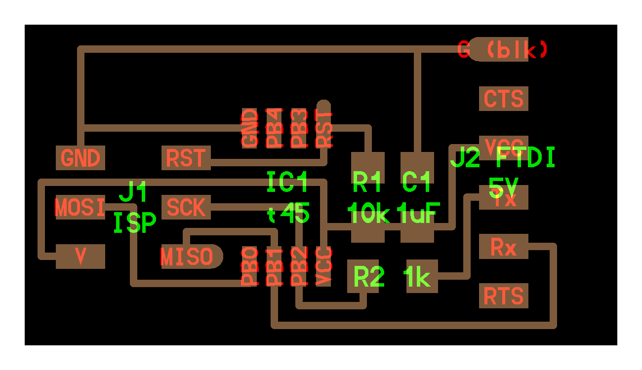
This week's assignment was to redraw an echo hello-world board,add (at least) a button and LED (with current-limiting resistor) check the design rules, make it, and test it.
I chose the ATtiny45 example.
To design the board from scratch and add the LED and button, we were taught to use Kicad on the local class on Thursday. Kicad is a wonderful cross-platform, open source Electronics Design Automation tool (EDA)
The first steps to follow when designing on Kicad, is to make sure all the symbols and footprints you want to use are available. For this, we downloaded a collection of fab-common symbols and footprints from the class website here, and some other common symbols like those from the ATTiny from Kicad's github page: symbols and footprints.
To do so, you go to the symbol editor on the main Kicad interface, and then go to Preferences > Manage symbol libraries, from where you can add the downloaded components so that they can be used on the design.
Once all the components are availabe, the first step was to create a new schematic, search for the necessary components from the ATtiny45 example, add an LED and a button, and place them anywhere.

The first thing i did was to replicate all the connections on the ATtiny example, leaving for now the button and LED apart. You do this by simply drawing wires using the W key from and to the pins.

Before connecting the button and the LED, i realized i had forgotten the resistor that would limit the current through the LED. So i added a resistor and proceeded to calculate it's value. Since i wanted to add 2 LEDs in series, i had to calculate the voltage drop of them both. I had to look at the LED datasheet, and search for how to calculate the resistance for more than one LED.
http://www.resistorguide.com/resistor-for-led/


So all in all i calculated a resistance of (5 - 1.8 - 1.8) / 0.02 = 70 Ohms But i ended up picking a 100 Ohm one to round up and to be safe. Although i had initially wrongly annotated 220 on the labels.
Once the resistor value was calculated, i proceeded to wire the extra part of the circuit, so i connected one lef of the button to VCC and the other to the LEDs with the resistance after these. But after talking to the instructors they said it would be better to connect it to one of the ATtiny's pins so that we could do something with it other than just turning it on or off, so i redrew the circuit with all these new elements connected to 2n pin (PB3) and the end of the resistor connected to ground obviously.

Once the schematic is ready, the next step is to generate the Netlist. This process saves a .net file that will be later on loaded by the PCBNew routing part. To do so, you just need to click on the Generate Netlist button on the schematics interface and click Generate Netlist - pretty straightforward. I left all the parameters by default.
With the netlist file generated, one can now jump to the hardest part of the process, which is to route all the elements. For this, from the main interface we need to create on PCB Layout Editor and create a new layout.
The first step is to configure the parameters that our board will have, such as the trace width. This will eventually determine the width of the copper paths of our board once it's milled, so it is quite important to take into account

Finally, you can load the netlist file with the button Load Netlist and you will generate what is very conveniently called Rats nest. Kicad will place all the elements almost on top of each other in a chaotic mess of pads and lines.

From here you can start moving the components to wherever you want them on the copper board, and you will see white lines that connect the pads of the elements that need to be connected. So when placing the components, you want to minimize these white line crossings. Otherwise, once you start routing the tracks, you will find yourself on deadlock situations where the only option might be to skip one line creating a bridge with a 0 Ohm resistor.
I was initially very optimistic about my newly acquired routing skills, and decided i would try to do a robots face where both LEDs would be the robots eyes, but after laying out the elements on what seemed the best possible option with the least amount of white line crossings and spending more than an hour trying to turn those connections into correct tracks, i gave up. I leave you with this capture screen capture though. Maybe next week i will give it another shot.

I then reshuffled everything and tried to place it similar to how the ATtiny45 example was, plus the new part of the circuit with the switch and the two LEDs. It wasn't an easy task either, but after a couple of tries, i managed to get everything connected. The last step once everything is routed is to draw the cut, in yellow, which will become the exterior image that the milling machine will cut.


Only later i realized i had chosen the wrong ISP connector, one that was meant to work on dual layer boards with holes, as opposed to having pads. So i had to go through all the process again. Luckily, Kicad has an update PCB function that will only load the changes you made, so after adding the new component on the schematics, i only had to remove the bad ISP connector and route the correct one on the pcb layout.
The very last step on Kicad is to export your design as SVG through File > Export. There are a couple of important settings to set:
- Black and white - so that you can turn it into a milling file with mods.
- All layers in one image - which makes it easier to deal with.
With the .svg on your disk, there's only two last steps before using mods to create the milling file: You need to export the 2 images (traces and exterior cut). To do so, i used illustrator to open the .svg and created an all-white layer to place under the traces. Then separated the outer cut on a separate layer, and i just exported to images by hiding the cut layer and the traces + white background layer.
The last step is to invert the colors of the traces image. I did this in photoshop, although you can also do this directly from within mods with an invert module.

With this, it all went down to the week 4 assignment, of milling the board, creating a shopping list with all the elements and then soldering. Sadly, once i had collected all the components while the board was milling, it came out like this, not thouroughly cut in many places. When i checked for connectivity with the multimeter, all those shallow cuts where communicating different tracks, and even though i tried to remove them with a cutter knife i wasn't able to do it. So i'll re-mill, solder and test it during next week because i ran out of time for this one.
