Group Assignment
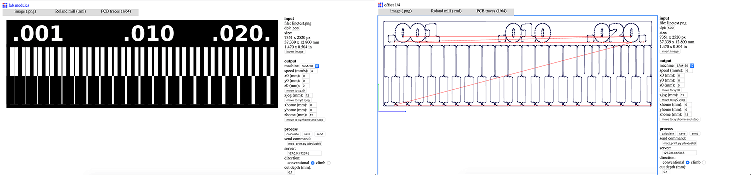
This week, in order to understand the machining process, I teamed up with these classmates: . The goal of this group assignment is for us to characterize the potential gaps between our traces, or how thin the traces could be. We used the Roland MonoFab SRM-20 machine to mill this test file. Detailed specs of the machine:
- Work area: 232 x 156mm
- Loadable workpiece weight: 2kg
- Operating speed: 6mm/min - 1,800 mm/min
- Operation strokes (x,y,z): 203 x 152 x 60mm
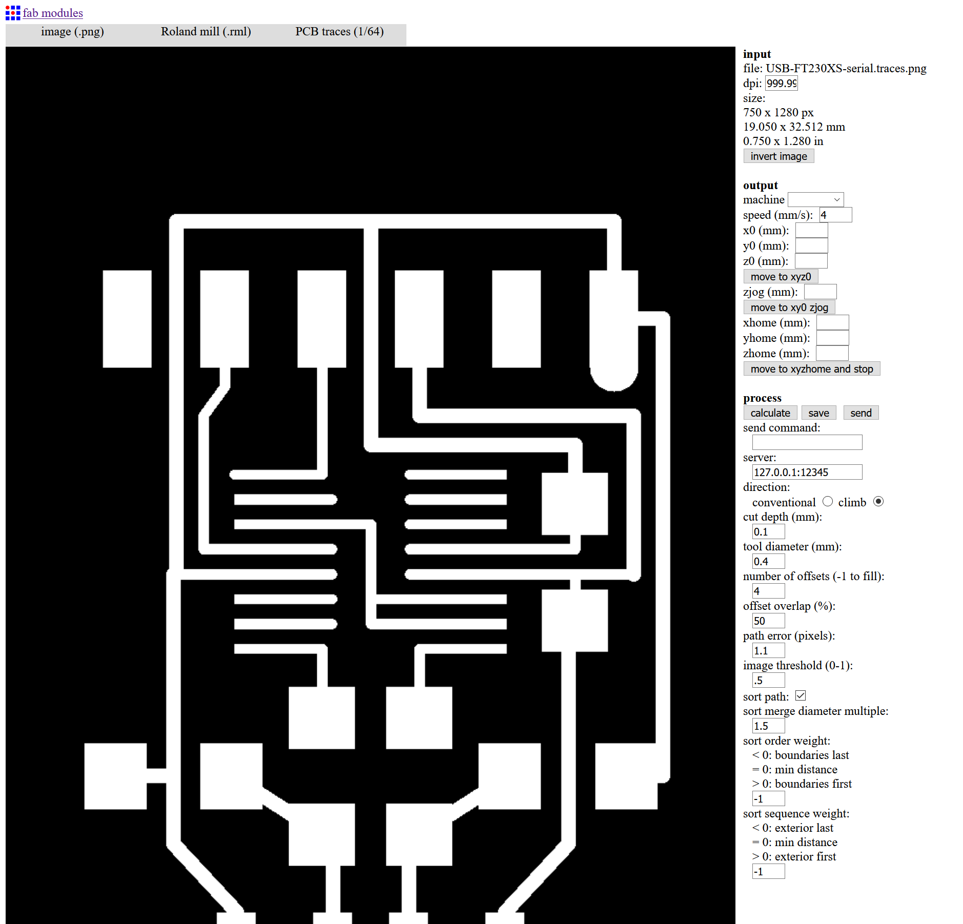
We prepared the .rml files using Fab Modules. The workflow of Fab Modules is pretty straightforward, and here are some recaps of steps followed:
- Select .png input format and load the .png files
- Select .rml output format
- Select the proper process: PCB traces (1/64) or PCB outline (1/32). This will automatically define the proper cut depth (0.1mm for milling traces and 0.6mm for cutting).
- Select SRM-20 in the output machine. Modify settings to origin 0,0,0 (x,y,z); zjog = 12 (to make sure the milling bit will be lifted up while moving across the workpiece and avoid damaging both the traces and the bit itself); and home 0,0,12 (x,y,z).
- Select the proper direction. If there are thin traces on the board, we need to select the conventional direction in order to avoid thin traces.
- Click the calculate button to calculate the toolpath and click the save button to save the .rml file.
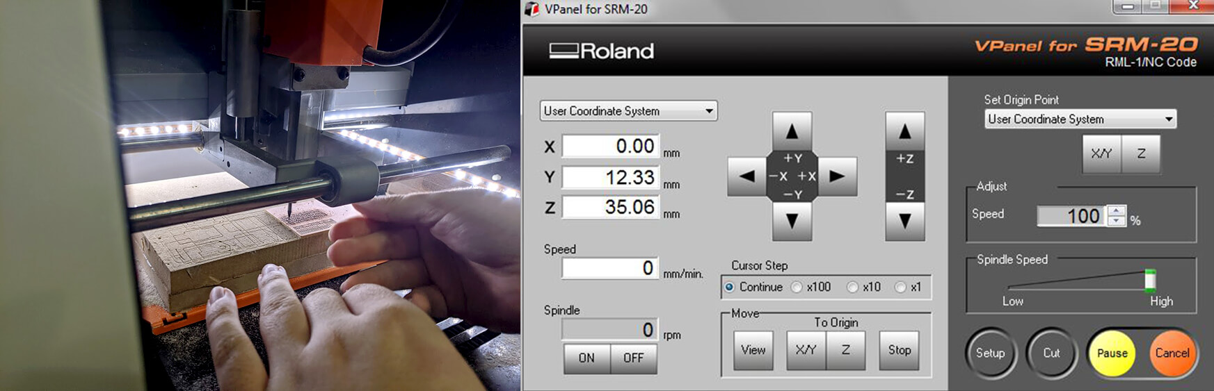
We used Roland VPanel controller to adjusting the milling start point, the feed rate, and spindle speed. Detailed summary of the steps to use the milling machine and VPanel controller:
- Choose the correct milling bit for the job. We were provided with 2 bits: the 1/64" used for milling the traces on the board and the 1/32" used for drilling holes and cutting.
- Insert the milling bit into the machine and manually adjust the Z origin.
- Set origin X/Y and Z in Vpanel. Click the Spindle button to test if the milling bit can cut through the copper layer.
- Click the Cut button to add the 4 .rml files and start milling!
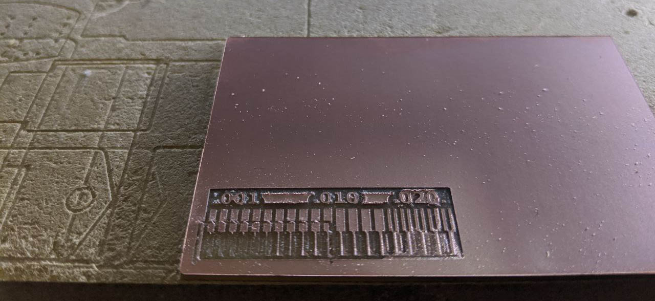
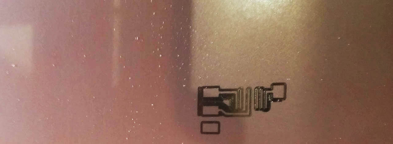
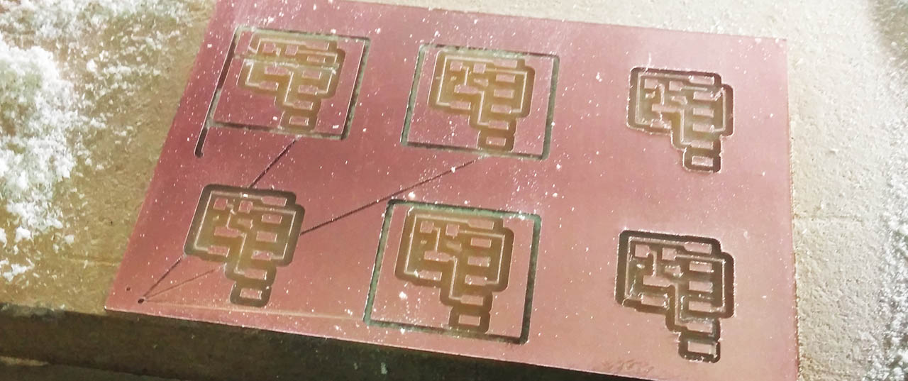
And here you go the result of the test:
Milling
The first part of the assignment was to mill one of the programming boards. We could choose from:
- FabISP
- FTDI / UPDI
- CMSIS-DAP / SWD Bridge
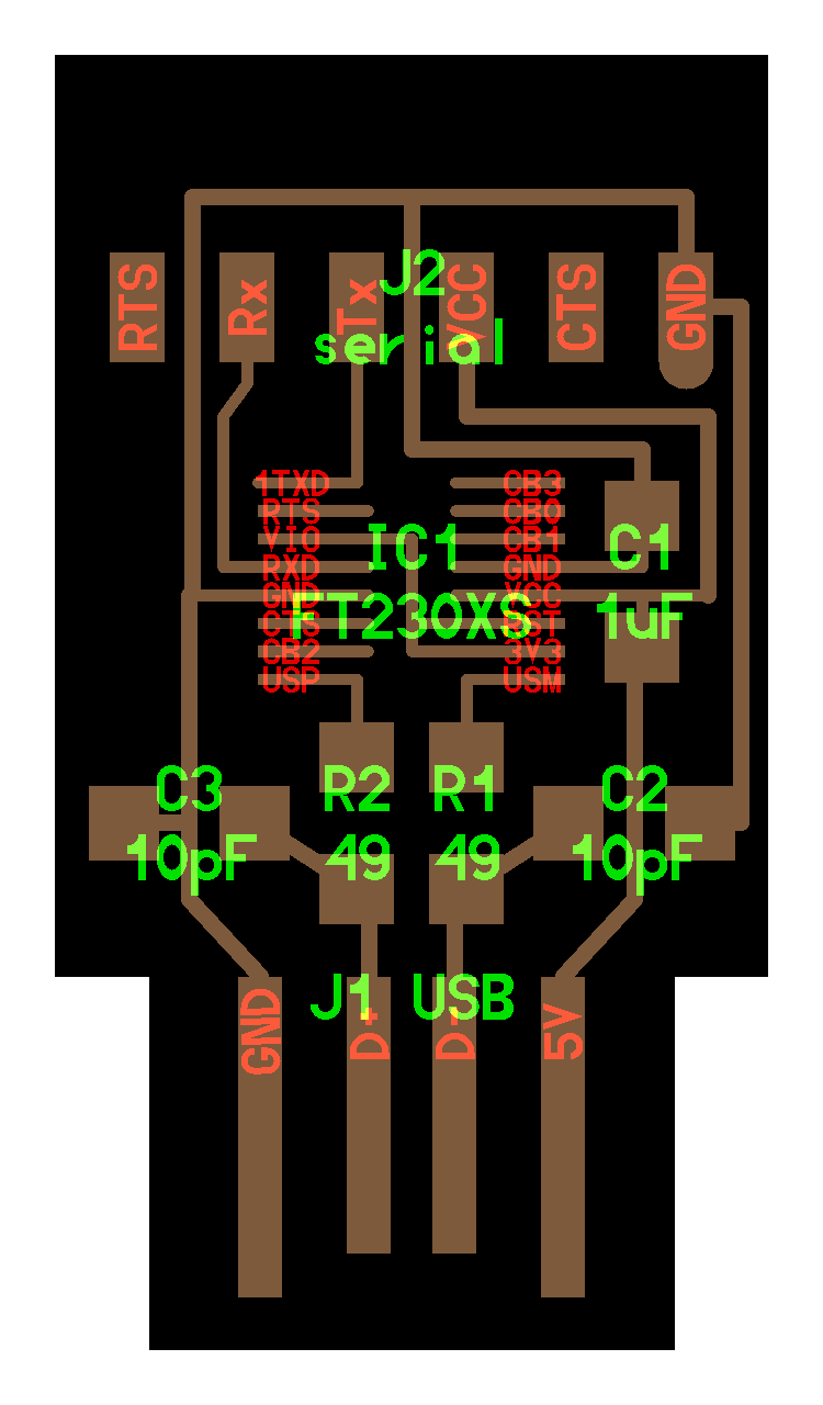
The first step was to download the images from the class documentation, where you can find:
- The schematics of the board
- An example picture of the soldered board
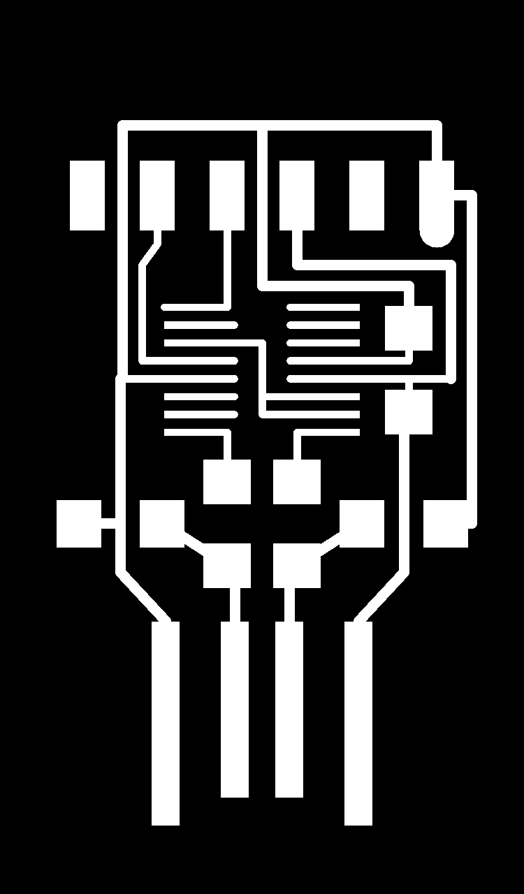
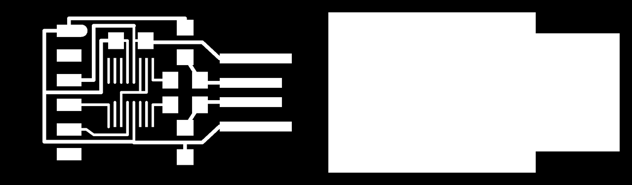
- An image with the interior traces that will be scratched
- An image with the outline that will be cut
For the milling of the board i used the Roland SRM-20 since it seemed much easier to operate. To start the process, i downloaded the images from the class documentation corresponding to the traces and the outline, linked above:
The software used to produce the file that the Roland machine understands (.rml) can either be MODS from CBA, or Fabmodules. To test both, i used mods to get the FTDI .rml and fabmodules to get the UDPI .rml. The process is quite similar, and they only differ in the layout that they use. While mods is a node-based graph, in fabmodules you sort of choose the process and parametrize each step, which seems more straightforward.
A few of the important parameters you set on both programs are:
- The image you want to process (obviously).
- x,y,z origin values - This are based on the origin set on the machine, where the header is placed where you want it to start on your material.
- zJog: The z height of the head when travelling.
- home x,y,z - where to go when the job is done, based on the machine origin again.
- You can also change the speed of the machine in mm/s or the number of offsets, to cut more or less, but we left them as they were.
In the case of mods, you just open the server program Roland > Mill > SRM-20 > PCB png and then add a file save module on the default Roland SRM-20 graph, plugged in the output of the calculate node, so that after calculating the routes, the graph would save the rml file to disk.
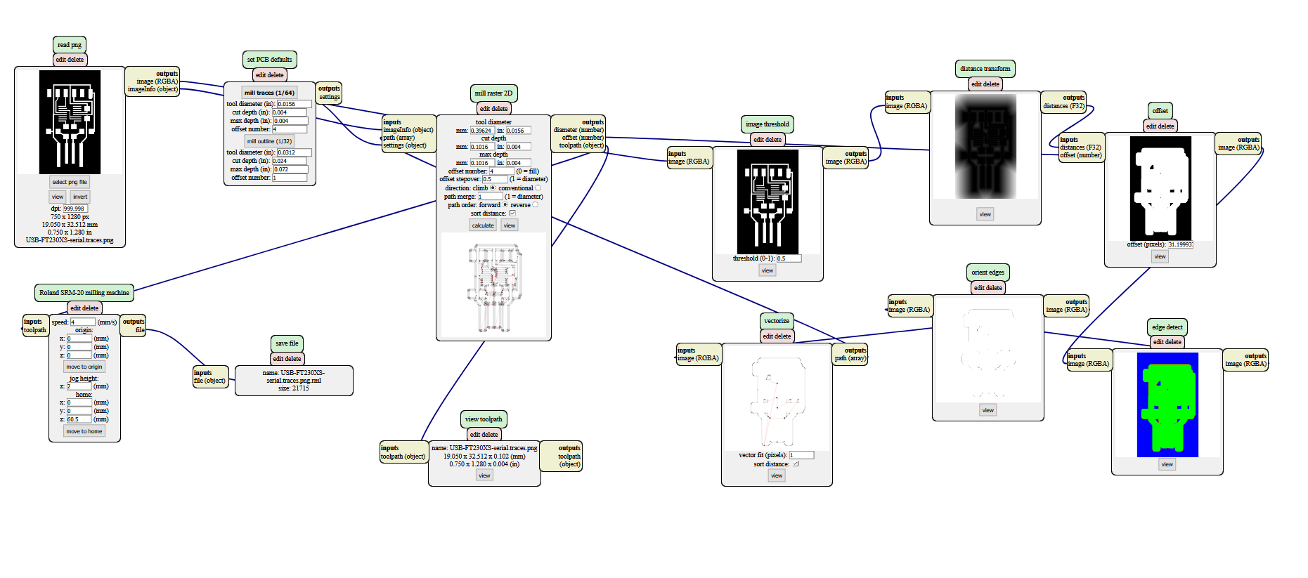
In fabmodules the process is different. You just choose the input format: image (PNG), the output format: Roland mill (.rml) and the process: PCB traces or outline. With each selection, the associated properties popup next to your image.
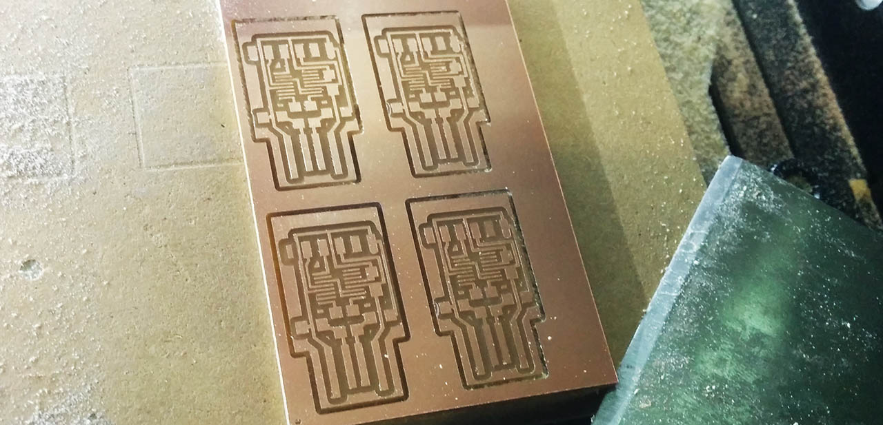
Once i had the files, i went to the Roland machine to load them up and cut. At this point, i teamed up with other members of fablab Barcelona to cut our boards at the same time, since access to the machines was not easy, taking into account that we are around 30 people (from fablab and IAAC's MDEF) and there are only two machines.
So we found out that in order to cut more than one board, you had to queue up different files, produced with mods of fabmodules with different origin values. We were told it was strongly recommended not to try to put all the boards in the same image. To queue up the files, you just simply add them one after the other on the add file menu on the Roland machine.
Before starting, we had to put the drill on the machine. We were kindly provided with one 1/64 and one 1/32 drills by the fablab staff to work with during the year. The 1/64 is used to cut (scratch) the traces, the interior, the 1/32 is used to cut the outline
The process to follow before launching the job is:
- Turn on the machine.
- Put the drill corresponding to what you are going to do.
- Move the machine to the origin of your material using the arrow buttons, and click Set origin XY.
- Move the head down with the up/down arrows until the drill is close to the material
- While softly holding the drill, unscrew it and bring it down until it touches the material.
- Screw the drill back on
- Spin the head and see if it is close enough to the material to scratch it.
- If it is, click set origin Z. If it isn't, lower the drill 1mm AT A TIME until the drill starts scratching the copper and set origin Z.
- Load the files, click Output, and cross your fingers !
At this point, while observing how the process was going, we hit pause after a while and then clicked on the View button, which brings the bed close to the window, to see how the process was going. We saw that the drill was barely scratching the surface, not deep enough to scratch all the copper away. So we had to take the drill back to the origin, lower it by a couple of millimiters and try again.
This time it seemed to work, so we let it work until it was finished. Once it was done, we brushed off the dust and alas! There were still some parts where the copper had not been fully scratched away... Damn.
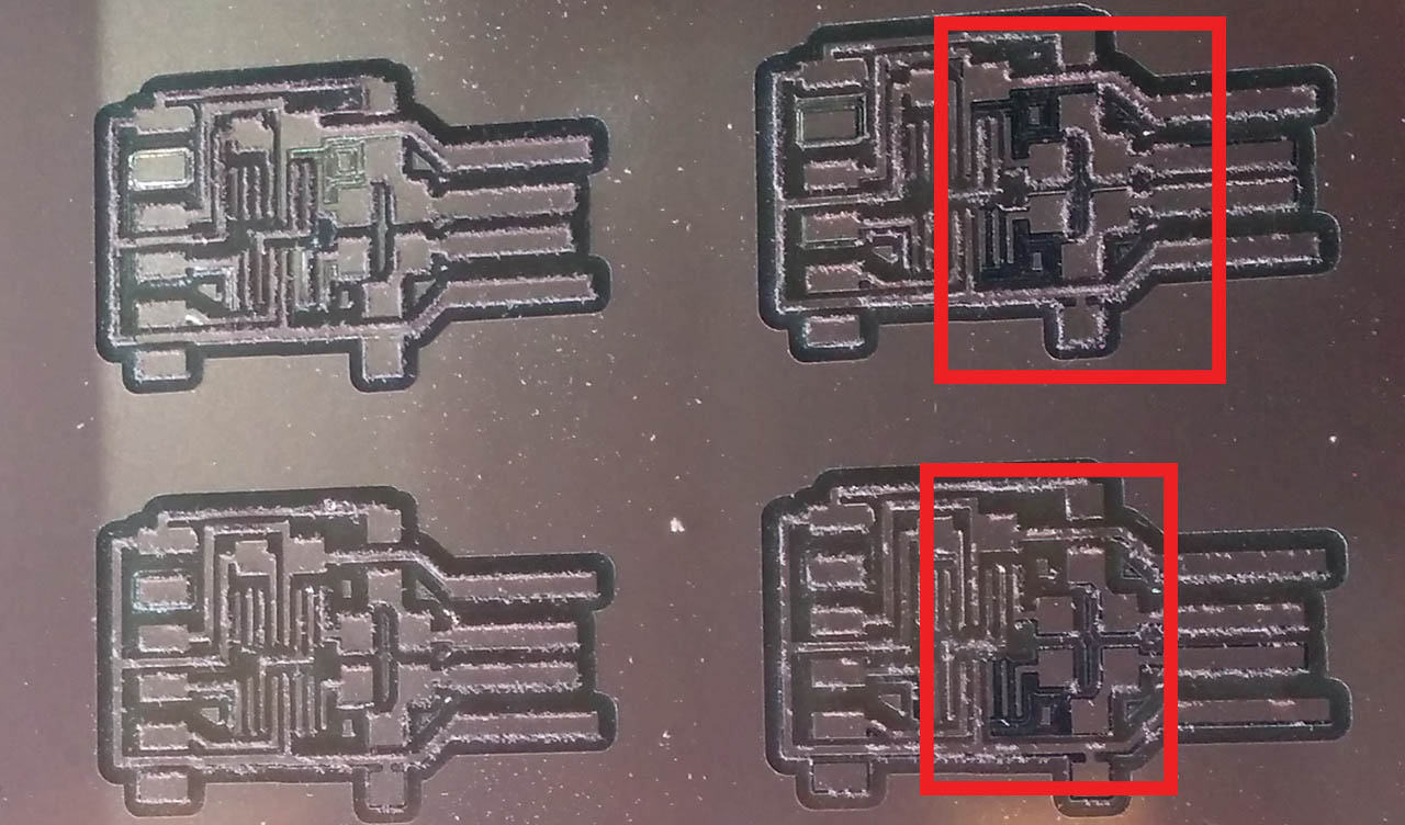
So here we go doing everything all over again, taking the drill to the origin and lowering the Z origin even more, and running the whole thing again. This time, finally, all the cuts were perfect and after changing the drill and running the outline files to cut, we could retrieve our boards
For the UDPI, we followed exactly the same process, making sure this time that the Z was low enough. And it was, all the scratches were being done perfectly, but once we came back to the machine, we realized this happened:
We had set the Z home to 0, so when the job was done for every file, it would go back to origin with a Z value of 0, basically scratching diagonally all over the board :/ Luckily, the cuts were not deep enough to cause any issue. We changed drills, and launched the outline. This time we realized that while cutting, the full copper board was moving a lot, so we press paused and asked our instructor Josep, who recommended we lower the speed. We set it from 100% to 30% initally and then 10% and the outline cuts were done perfectly.

Soldering
With the boards freshly cut, it was time to start soldering. A good starting point, emphasized by our instructor Edu, was to create a shopping list with all the components, taken from the schematics image link in the previous section, fetching each element from the supplies and sticking it with tape next to the shopping list.
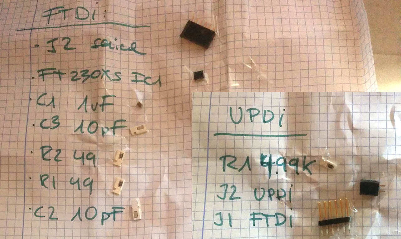
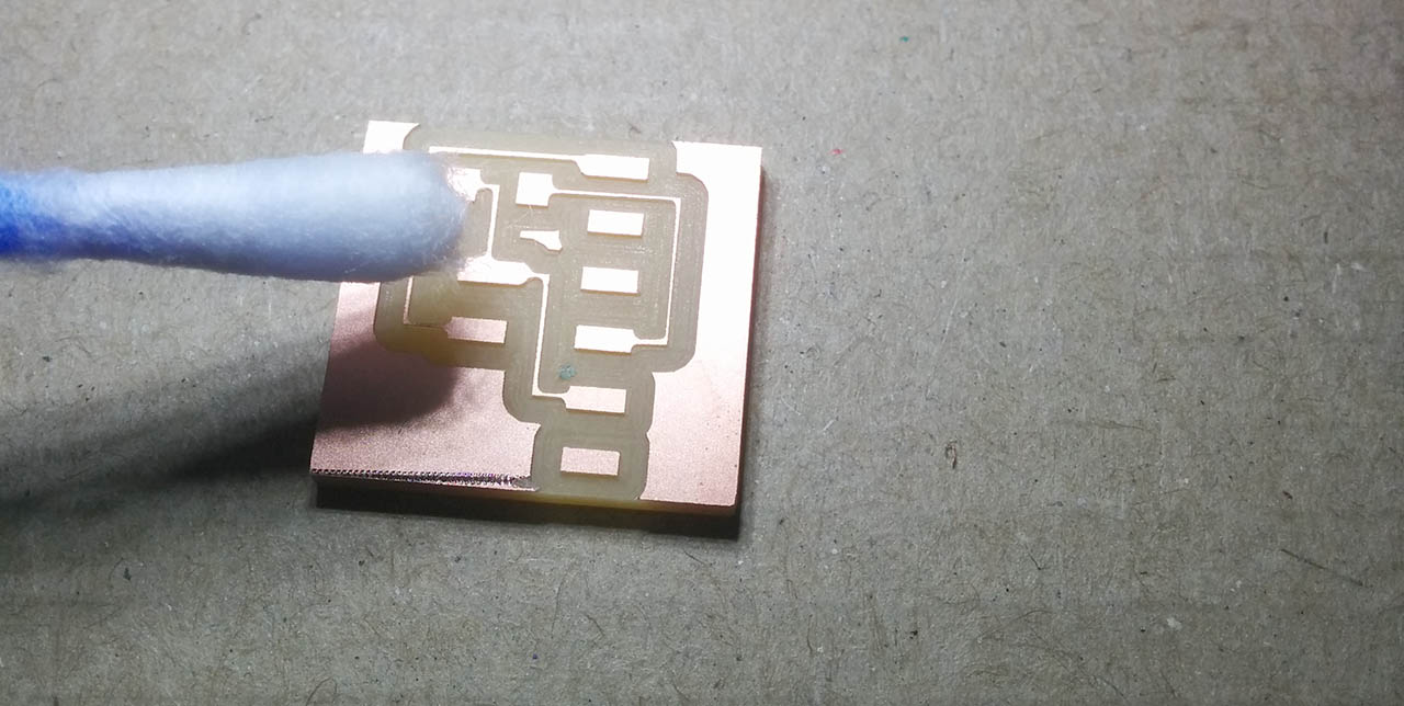
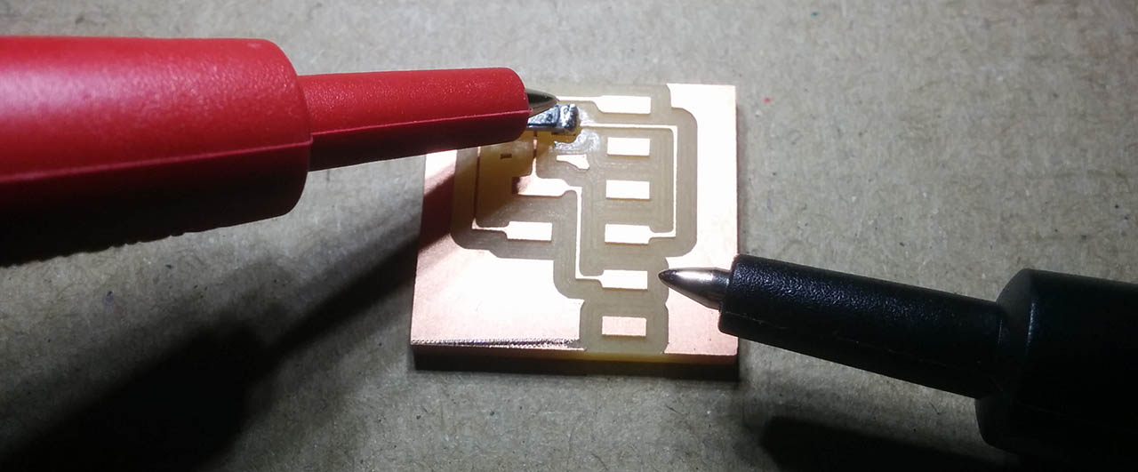
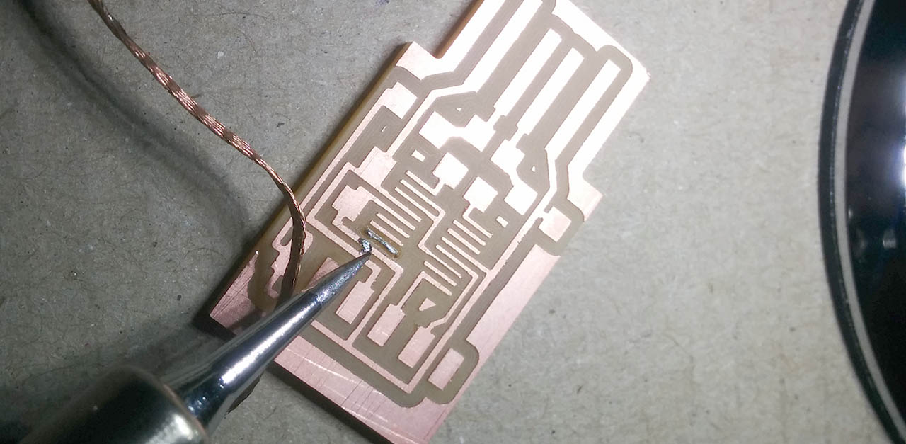
Another good practice before starting to solder, is to clean the whole board with alcohol, and test for continuity problems on the copper traces. I realized that cotton swabs might not be the best thing, since they leave tiny fiber traces on the board
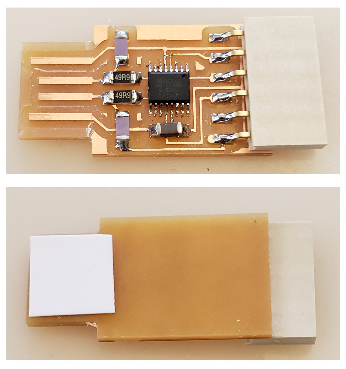
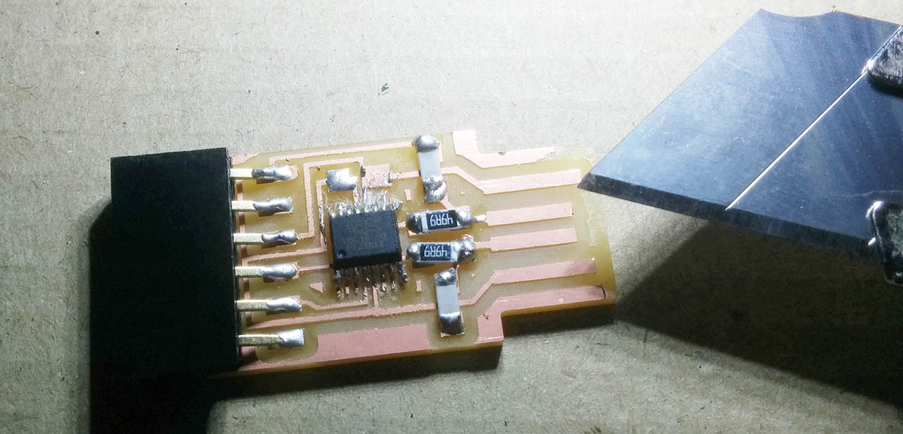
I started by soldering the UPDI board since it seemed much easier. Everything worked on the first try here, although as you can see it is far from good looking. I was also checking for continuity after each element was soldered, to catch errors as early as possible, since correcting solders is much easier when there's not much stuff around.
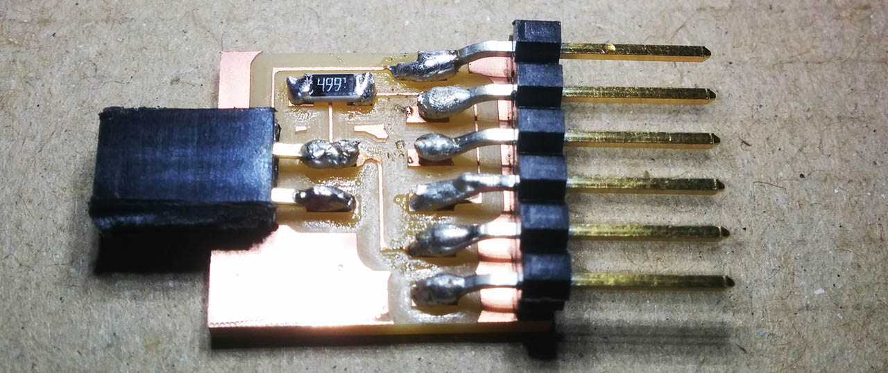
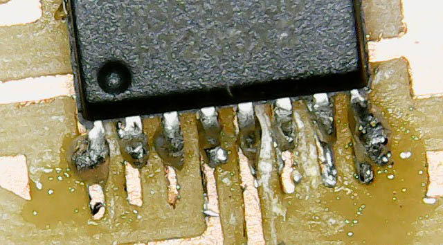
Then i switched to the bigger FTDI. It's a good strategy to start with the smallest, more complex components, and then work your way out to the biggest simple ones. In the case of the FTDI, the hardest one is by far the microcontroller, which has super small pins. A good way to start is by laying out a line of solder and placing one pin of the component to fix it, so that soldering the rest of the pins becomes easier as it stays in place.
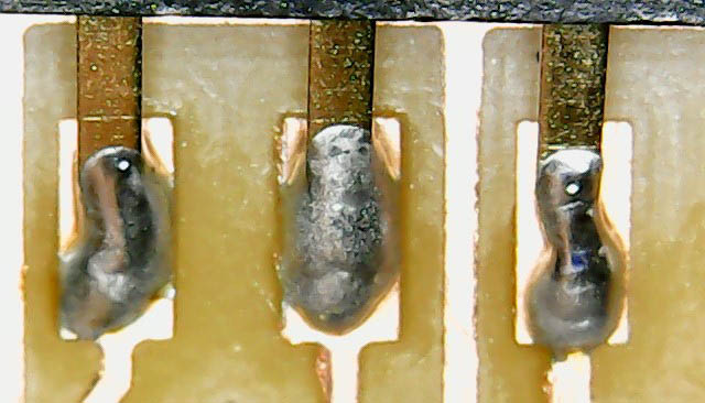
At this point (so early!) i had the first issue, where some solder was spilled on the copper trace next to the pin one. While not terrible since it is not crossing any other lines, i used copper braid to remove it.
Then i started trying to solder the first pin, to make it stay in place, and then the pin on the opposite side of it, to keep it there. Soldering the rest of the microcontroller's pins was a challenge and a mess. They're so tiny that it was really hard to get only one, so in the end it was easier to solder a few together, and then play with the solder, moving it around, until each pin was isolated. I found that using a fine tip for the solder was very convenient for this, although i ended up scratching the board a lot.
The rest of the board was much easier to solder, as the resistors and capacitors have very large pads, compared to the microcontroller, and the connectors have their pins way more spread out. A good strategy is to drop a drop of solder on the pad, then bring the component in with the tweezers while you heat it up again with the solderer until it's attached, and finally soldering the other end by bringing the solderer and tin together.
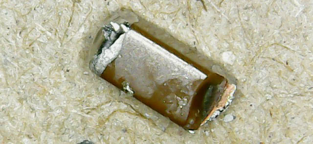
Regardless, some of the resistors ended up being not straight, and i somehow managed to break a capacitor. I guess from too much heat ? So i had to go fetch a new one and solder it back in.
The last solders ended up looking much better than the first ones :)
The last step was to remove the outer cut of the copper on the board on the side of the usb connection. I did so by using a cutter and very gently and slowly scratching it away. In hindsight, i should have done this before anything, since a couple of times the cutter slid and it touched a component. Luckily nothing got broken, so after checking for continuities, the board was ready to test.
Finally, it was time to test the board by plugging it into a PC through a USB extension cord. To do so, i had to attach a bit of paper on the bottom of the board, to adapt to the height of the connection. Once plugged in, it showed up in the windows device manager, under the Universal serial bus controllers category.
Today i learned
- Calibrate the Z axis on the milling machine well. It can save a lot of time and headaches.
- Pause the job a few seconds after the start to double check everything is working as opposed to checking it when it's done.
- Remember to set zJog and the home Z to > 0 values, or you will scratch the board when the drill is just moving around.
- Lower the speed while cutting the outline to reduce board vibration.
- I thought a fine tip solder would work well for general soldering at this scale, but in the end found that it takes too long to heat up the tin filament or the copper braid to remove tin, so i changed it to a regular one.
- It's much better to cut off the excess copper from the board before you do any work on it.
- It's very convenient to check for continuity on each component separately after soldering it, as opposed to checking everything at once for the first time.
- For the super tiny microcontroller pins, after talking to colleagues, it's easier to solder all of them at once, and then work the excess tin out of it until the pins are isolated.