7. Electronics design
This weeks group assignment is to use the test equipment in our lab to observe the operation of a micro controller circuit board. And as individual assignment we have to redraw the echo hello-world board, and add (at least) a button and LED (with current-limiting resistor). Important is to check the design rules, make it and test it. For extra credits you can simulate it operation and render it.
Files, planning and tools
Files
Planning
- Redraw the hello echo circuit file from Henk
- Add an extra LED
- Use the Modela to mill the board
- Solder the board
- Test the board and check the soldering
- Program the board with the Hello Echo program
- Use the test equipment to test my board
Tools
- KiCad
- Gimp
- Cloud convert
- Mods
- Roland Modela MDX-20
- Soldering iron
- Multimeter
- Arduino Uno
Link with final project
First I thought I would create a leaf shape circuit so it would be linked to my tree theme but in the end the electronic part is more related to my interaction spirals. And I wanted to see if I could fit the components nicely and efficient on a square.
Research and inspiration
This week I mainly researched and looked into tutorials about PCB design, routing and trouble shooting. Autodesk has useful tips for beginners and PCB design. In the end most of my time and research this week went into trouble shooting the error “initialization failed”
In addition I went to the museum Speelklok to get inspiration for my final project this week. This museum shows the wonderful world of self-playing musical instruments. They have an historic collection with organs, automata and playing boxes. On Sunday it was the last day of their exhibition Robot Loves Music.
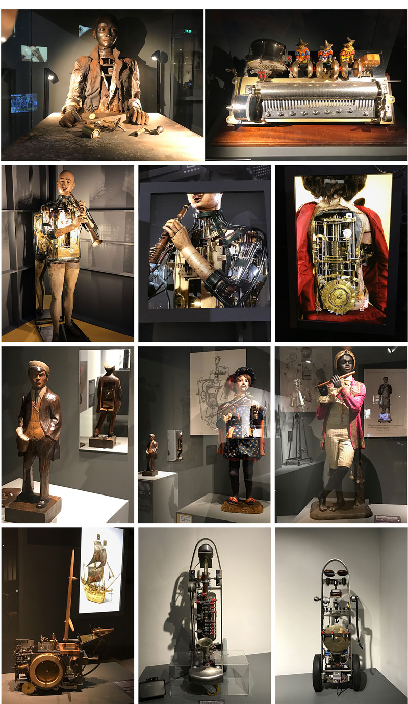 Robot loves music exhibition at the Museum Speelklok
Links used for design and routing my board
- Autodesk: top 10 pcb component placement tips for pcb beginner
- Autodesk: Top 10 pcb routing tips for beginners
- Cloud convert
- KiCad
Links used for programming my board
- High-low tech: Programming an ATtiny w/ Arduino
- Arduino as ISP and Arduino Bootloaders
- HELP!! I;m running avrdude and I get “Initialization failed, c-1”
- documentation of Fab Academy student Andrew Sleigh
What we did – Group assignment step-by-step
On Thursday Henk showed us how the test equipment in our lab works with the use of his hello echo board from last year. I still find it difficult to totally grasp the way to use them. However this week I did get used to working with the multimeter and testing the circuit. I still have to get more used to the oscilloscope and power supply.
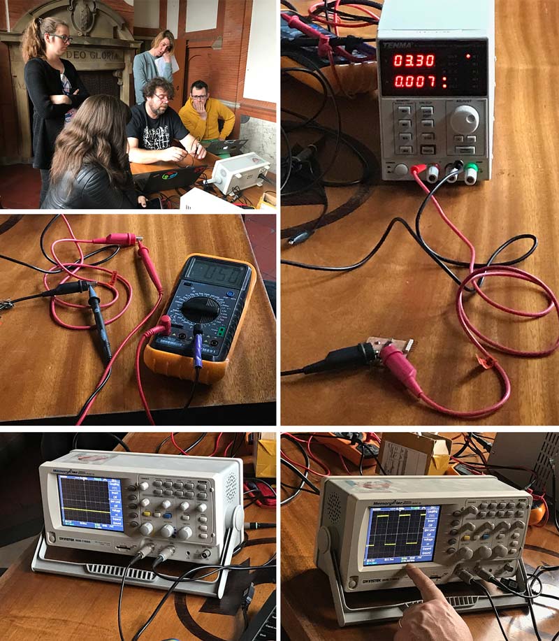 How to use the oscilloscope, power supplier and multimeter
When and why use these test equipments
The Power supply: this equipement is useful to power your board. It’s more useful than battery when ypu’re debugging because you can control the voltage. And you can make sure the voltage matches the circuit. You can also use it to measure the power of you circuit by connecting your board.
Oscilloscope: The main purpose of the oscilloscope is that is graphs the electrical signal as it varies over time, this way you can measure the timing of the board. This is useful for testing the resonator for example. I still find it hard to totally grasp the concept of how to work with it, however the tutorial by Sparkfun helps for a beginner in electronics and when and why to use the oscilloscope.
Multimeter: We used the multimeter in week 5 as well, however this week I got a better understanding of its use. You can easily check your circuit board for shorts, you can check if the wires and components are connected the way you designed.
What I did – step-by-step
For this weeks individual assignment Henk gave us his electronic schematics from last year. He wanted us to redraw it.
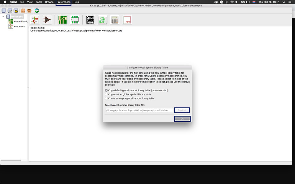
Step 1: drawing the schematics in kiCad
I used Henk schematics from last year copied it and added a green LED with an extra resistor. Because I wanted to add something myself and I saw one pin, number 5, was still free. I’m not sure if this will work, I did check the data sheet and as far as I understand I can use this pin, number 5, as an out for the timer like pin 6 which is connected to the red LED.
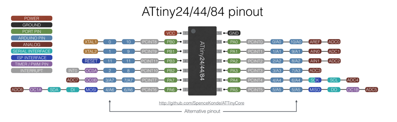 The pins on the ATtiny44
In total the extra components added to the Fab Academy Echo board are:
- Red LED
- Green LED
- 5k resistor
- 499 resistor
- Button (switch)
- Phototransistor (sensor)
 Step 1: Adding components to kiCad - add library to kiCad for new file
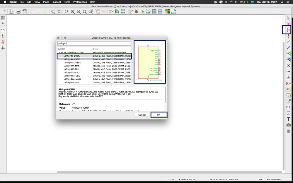 Step 2: Adding components to kiCad - select components add to drawing board
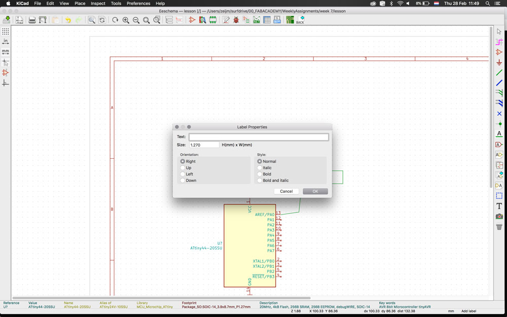 Step 3: Adding components to kiCad - label properties
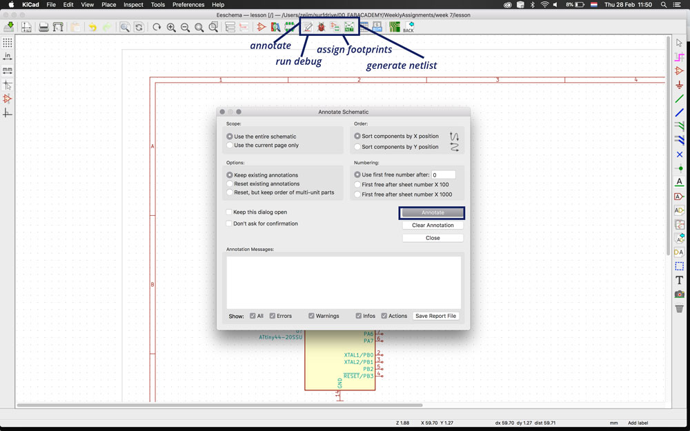 Step 4: Adding components to kiCad - annotate components
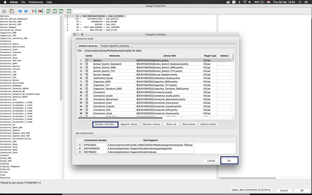 Step 5: Adding components to kiCad - add footprint
- Download the library from the Fab Academy for kiCAd
- Open schematic layout editor.
- Go to preferences > manage symbol library > add the Fab library to kiCad.
- Select Place tool > choose the component from the library and place it on the board.
- Follow this step for each of the components.
- When I placed all my components I added a wire (hot key: W) with a label (hot key: L) to each of the component.
- Annotate the components with meaningful labels.
- Assign the right footprints to the components > first download the Fab library in the footprint manager. This way you select the right components from the Fab lab inventory.
- Run
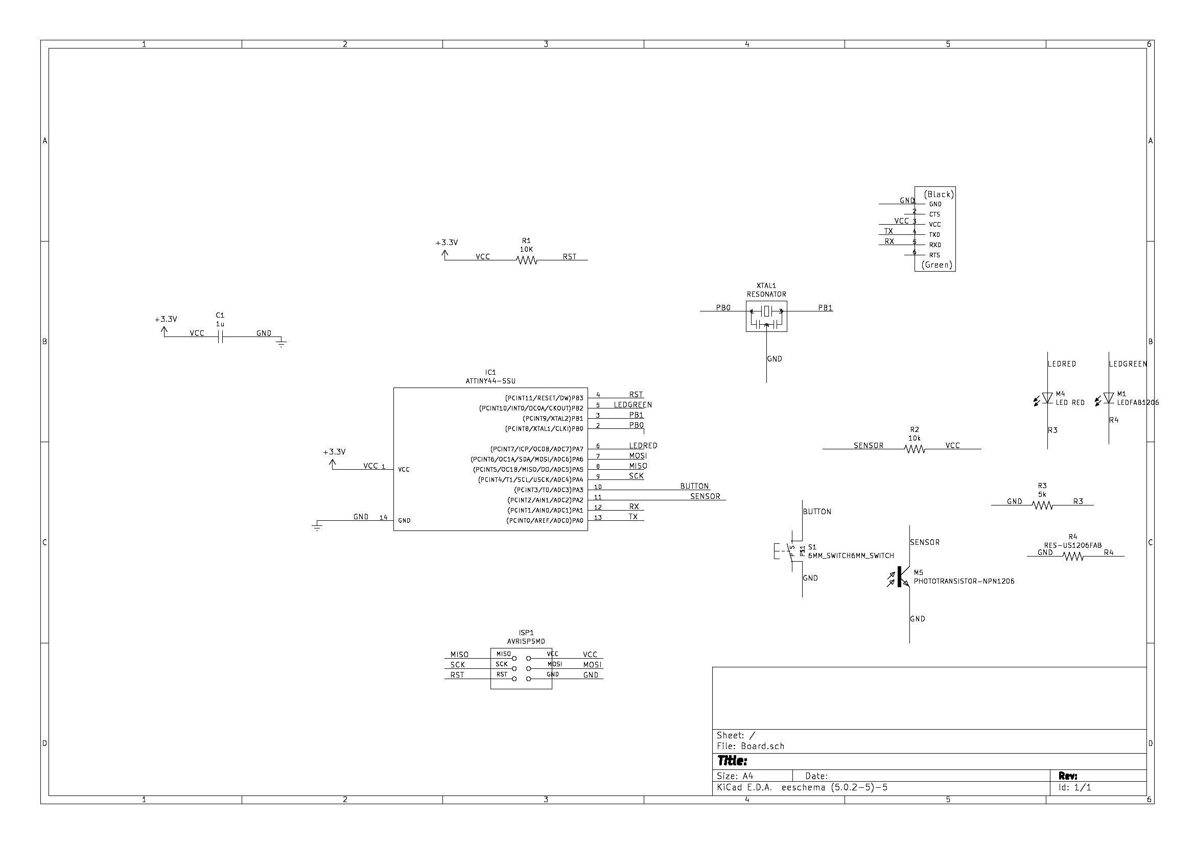 My final schematic of my echo board
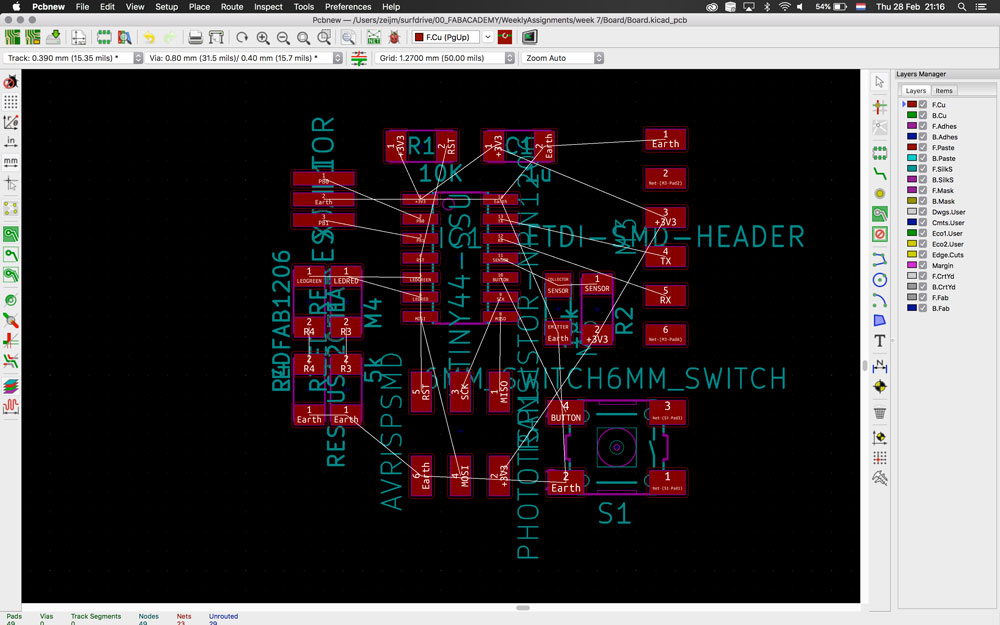
Step 2: placing the component and route the PCB in kiCad
After imported the schematic in the PCB editor I first played around a lot with the placement of the components. My initial idea was to place them in a leaf shape but in the end all the parts where not efficiently connected. So I wanted to make my board as efficient as I could make it. While I was designing my board I kept these rules in the back of my mind:
- Know how the component look like, because this determines their place on the board.
- The FTDI-header should be on the side with the pins in the right direction.
- ATtiny44 in the middle make sure all the legs and the components connected to it don’t cross over in lines
- The ground and vcc can crossover with lines as long as I can find a way for them to go around the board or through the middle.
- Don’t forget to adjust the design rules in the PCB editor to the design rules of the Modula at the Waag.
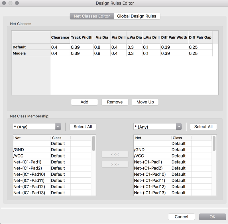 Settings design rules
I read in the Autodesk: Top 10 pcb routing tips for beginners that for PCD design “90% of your time goes into placement and 10% into routing”. I took this advise I took my time to place the components before I started routing.
In the end I looked at the basic design of the Fab Academy echo board and used this as starting point and added the six extra components. This was still a bit of a puzzle especially with connecting the VCC and the switch. Till I realized I could use the space underneath a component as well. So I connected the button while going underneath the photo transistor and I routed the VCC under the button. This way it was connected efficiently.
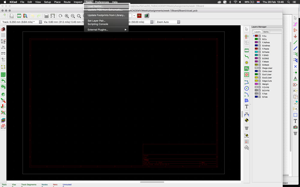 Step 1: From schematic to PCB design - Load netlist
 Step 2: From schematic to PCB design - Netlist loaded
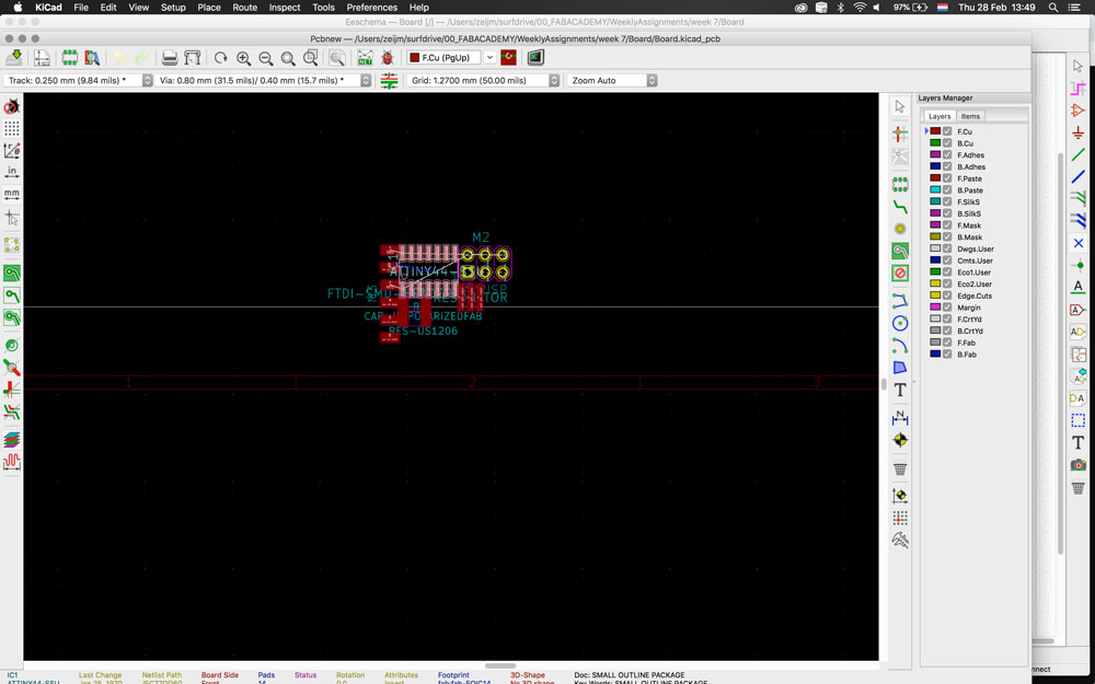
 Step 3: From schematic to PCB design - Move parts
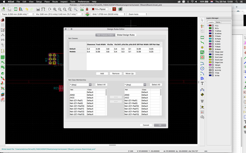 Step 4: From schematic to PCB design - Set the design rules
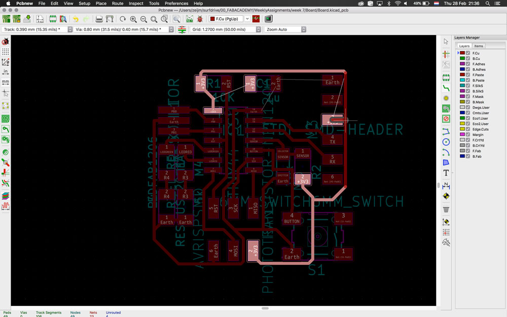 Step 6: From schematic to PCB design - Route circuit
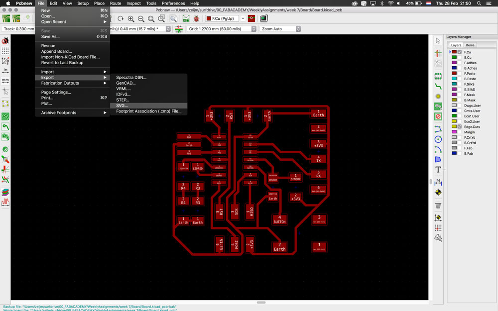 Step 6: From schematic to PCB design - Export file as SVG
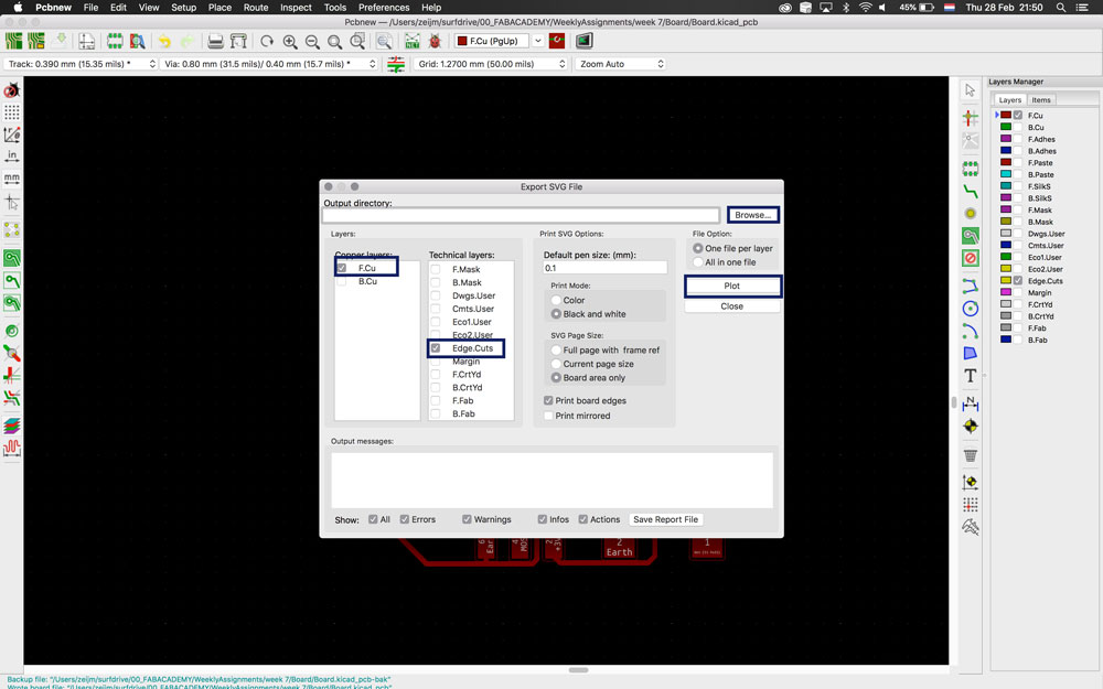 Step 7: From schematic to PCB design - Plot file
Step 3: exporting the file to SVG and save as png
I had some troubles saving the file as png. Because it wouldn’t open nicely in illustrator therefore I used Gimp. However when I opened my file in Mods I saw that the dimensions of the PNG didn’t fit the dimensions in kiCad. When I opened the file in Gimp again I saw that it gave the message: “SVG file doesn’t specify size”. In the end I used Cloudconvert and later on Photoshop to adjust the color and resolution of the PNG file. More details about the trouble shooting can be found at the “what went wrong” section.
- Go to Cloudconvert
- Select file > choose PNG > download file
- Open it in GIMP
- Remove alpha channel
- Invert color.
- Export again as PNG
- Open it in Mods and double check is the size is correct.
Step 4: milling the board
I used my own documentation from week 5 for milling my board with using Mods and the Modela. It had the right settings and work flow. This went fine with no problem. So I was happy when I saw my board finished until I looked closely and saw that my lines where connected to the footprint at more than place. So I had to go back to the drawing board.
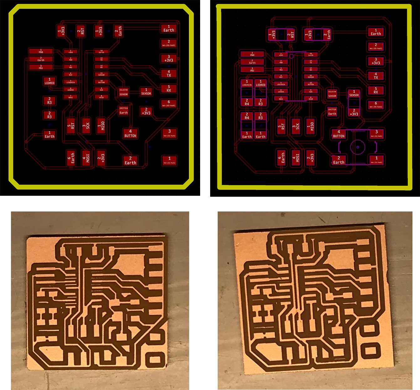 Board 1 and 2
Step 5: changing the design and mill again
I found out that I forgot to change the clearance in the design rules. I did change the other rules but forgot this one. The default was 0.2 while it should 0.4 for our milling machine. So I changed this and in kiCad it showed that the lines where ticker so I had make my board a bit bigger and I moved my lines so they would have more space around it. For the ones that were on the edge it was easy to fix because these got more space by making the board bigger. But I was a bit scared that the three lines (RST, GRD and SCK) wouldn’t fit underneath the ATtiny 44 anymore. But it looked fine the design, they fitted.
Still connecting lines
When I finished my redesign I milled it again. This time I didn’t have the problem with a lot of lines sticking to the footprint. But in the end, the three lines mentioned above did connect. Because I didn’t want to start over again and I saw there was space to disconnect these three lines from each other I used a knife to disconnect them.
Step 6: testing and soldering
Before I started soldering I triple checked my connection and lines.
Testing my board
- By eye, look closely at your board are there connections you don’t want. Good trick is to look at your board against the light. This way you can really easily see if there are lines connected you don’t want
- Triple check the lines with the multimeter. As mentioned in week 5 you can use the multimeter to check your board. By placing the pins on a line you can hear if it creates a short. I used the multimeter a lot for checking my three lines to make sure they really aren’t connected before soldering.
Soldering my board
After my test I soldered my board, I did this at home. First I collected all the components. I decided in which order I would solder my board: from inside out, low to high.
Order of soldering:
- ATtiny44
- Photo transistor and its resistor
- Resonator
- The two LEDS with their resistors
- The resistor and capacitor on the top
- ISP header pin
- Button
- FTDI-header
The soldering didn’t go as smooth and shining as week 5. I soldered at home and somehow the tip of soldering iron didn’t heat up as well. In addition the tip still had a flat top while the one at the Waag has a needle top, which is much more precise. But in the end I managed to solder all the parts.
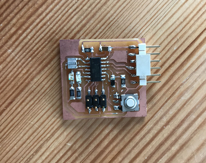 My echo board soldered
Step 7: testing my board
The testing of my board took a lot longer than I thought based on the experience of Joey and Henk. In the end it took me a full day to trouble shoot and trying to find out what was wrong. I started with the notes from Joey so I frest followed the steps he took. However I got an error after the checking if I could talk with the ATtiny44. From there on I started a debugging spree.
Check if my computer can see the programmer
So I first used the command: ioreg -p IOUSB
I got a simular result as Joey
ioreg -p IOUSB
+-o Root  <class IORegistryEntry, id 0x100000100, retain 15>
  +-o AppleUSBXHCI Root Hub Simulation@14000000  <class AppleUSBRootHubDevice, $
    +-o Bluetooth USB Host Controller@14300000  <class AppleUSBDevice, id 0x100$
    +-o USBtinySPI@14100000  <class AppleUSBDevice, id 0x100039f34, registered,$
C02QL5F2FVH5:/ zeijm$
I also double checked my system profiler and it would recognize my usbtiny. So I knew that at least my computer saw my programmer.
Check if the programmer could talk with the ATtiny44
For this I used the command: avrdude -c usbtiny -p t44 This didn’t go the way it should as I got an error.
avrdude: initialization failed, rc= -1
	Double check connections and try again, or use -F to override this check.
I was working from home so I could try other usbtiny’s or try to solder something else. So I was really eager to solve this error on my own. I describe my debugging process below. In the end it was the soldering bridge from the programmer that was the cause of the error.
What I did wrong – and how I solved it
Export SVG kiCad and Gimp
From kiCad I exported a SVG file. I used Gimp to convert my file to a PNG but when I opened this file in Mods it displayed incorrect sizes. When I opened the SVG file in Gimp for the second time I saw that the pop-up shows the message: “SVG file does not specify a size”.
- First I double checked my settings in kiCad. And exported it again to check if something went wrong in the export. This still gave the same problem.
- Luckily Joey arrived and he used Cloud convert to convert his SVG to PNG. So I tried this as well. This option kept the right sizes.
- After I had the right sizes I opened the PNG file in Gimp again, this time with the sizes where still correct. So I removed the alpha channel and inverted the color.
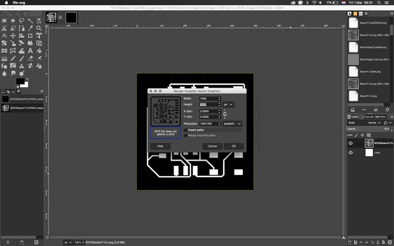 Importing SVG file into Gimp
Don’t forget the design rules.
When my milling was finished I saw that some lines were connected to the footprint. While I was designing in kiCad I thought I set the right margins. I double checked the design rules when I set them but in the end I forgot the first part, which was the clearance. This should be set to 0.4.
With routing and placement of the component use this margin wisely as in the end I still had three lines connected to each other. So for the next time make sure there’s enough space between each component and each wire.
Check your tip
While soldering I found it difficult to be precise. The tip wouldn’t heat up. While checking it I found out that with changing tips I didn’t place it all the way down. So it couldn’t get enough heat. In addition I the tip was ticker than the one I used at the Waag. This made it more frustrating to get nice a precise soldering.
Error: Double check connections and try again
When I wanted to check and communicate with my board I got the same error all the time.
Invalid device signature. Double check connection and try again
It took me more than a day to trouble shoot. I looked into all the possible options what it could be. The tutorial: HELP!! I’m running avrdude and I get “Initialization failed, c-1” gave me steps I could follow for my trouble shooting.
Debug 1: Check board:
First I checked my board again to make sure there weren’t any shorts and that all that the pins are connected with the right components. I used the multimeter and this all checked out.
Debug 2: USB 2.0 HUB
I thought it might be the USB 3.0 port on my mac as this was the problem previous time. So I used an USB 2.0 hub to see if this would help. It didn’t I still got the same error.
Debug 3: timing of the board
I added the -B to my command. This changes the clock speed. There is a difference in the error message when I used the command -B or not. When I use -B and lower the clock speed the Error rc=1 error doesn’t appear anymore and the device does give an signature ‘Device signature = 0x02fd45’ in stead of 0x000000. However in the end I don’t know what it really means and if this really is something useful for debugging. Because the results are quite random as the Device signature changes every time I run the command.
"C02QL5F2FVH5:~ zeijm$ avrdude -c usbtiny -p t44 -B 250

avrdude: AVR device initialized and ready to accept instructions

Reading | ################################################## | 100% 0.05s

avrdude: Device signature = 0x000000 (retrying)

Reading | ################################################## | 100% 0.05s

avrdude: Device signature = 0x000000 (retrying)

Reading | ################################################## | 100% 0.05s

avrdude: Device signature = 0x02fd45
avrdude: Expected signature for ATtiny44 is 1E 92 07
         Double check chip, or use -F to override this check.

avrdude done.  Thank you."
Debug 4: Check my board again
So I started with checking my board again for shorts and connections and possible soldering mistakes.
- Is the ground connected everywhere where it should? Yes.
- Is the VCC connected? Yes and they don’t give shorts
- Are all the pins are connected
Debug 5: Check my cable
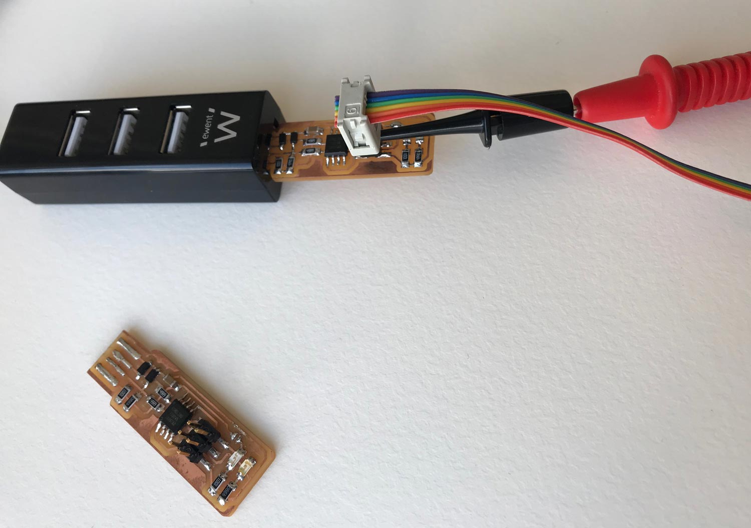
I made my own ribbon cable, it could be that somehow my cable didn’t have the right connection. So I place the cable in both my Fabisp and my board. I used the multimeter to check each pin and if they made an connection from one board to the other. The connection and the cable both were fine. They worked.
Debug 6: Check if it’s the programmer
Next step was to check if it might be used my Arduino as and ISPprogrammer to make sure it wasn’t my FabISP tinyusb programmer that was broken. To be able to set up an Arduino as programmer you first have to set it up and load an sketch into the Arduino so it’s know it functions as a programmer. I used the documentation of Andrew Sleigh Fab Academy student of 2018 I followed his steps. I also added the ATtiny44 to the boards. I run the boot loader. But again I got the same error. Somehow I still got the idea I did something wrong, I used the tuturials: High-low tech: Programming an ATtiny w/ Arduino and Arduino as ISP and Arduino Bootloaders. Double check my steps.
Debug 7: Retracing steps
I retraced my steps again, starting with the schematics from Henk, my design, my wires, my board. Every check seemed fine, so the only thing I could think of was that maybe I fried my ATtiny44 while soldering my board. However I wanted to be sure this was the problem before starting to solder again.
 Trouble shooting the Fab usbtiny programmer
Debug 8: Double check with Joey
The following day I asked Joey, who works at the same university, to bring his board and programmer since it worked fine for him. This way I could double check what part would be the problem. We found the problem really fast.
- Check USB > Joey’s laptop registered the FABIsp
- Use the
avrdude -c usbtiny -p t44to make a connection to the ATtiny44. And it worked straight away. No problem at all with the use of Joey’s programmer and his ribbon cable. - So we double checked if the cable was the problem, this turned out to work OK with mine as well.
- After that we double checked with my programmer and his computer and he got the same error as me.
- We wanted to figure what the problem could be. The only difference between our programmers is that I de-soldered the connection to the red LED and Joey didn’t. So we thought this might be the problem as that’s the only difference between the two. First we used the multimeter but this didn’t give a definite answer.
- I soldered the connection back on my programmer and tried again. And this time the
avrdude -c usbtiny -p t44command worked with my programmer as well. - To make sure this really was the problem, Joey de-soldered his connection and used the command and he got the same error I had all day yesterday.
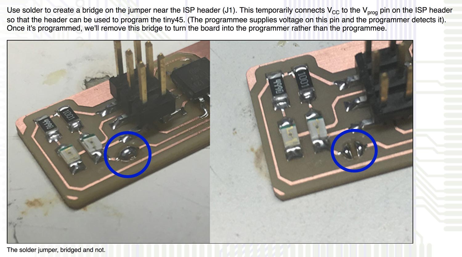 This is where it went wrong. The last step of Brian’s FabTinyISP tutorial
What I learned
How to really use the multimeter
This week I really learned how to use the multimeter. While debugging and trouble shooting my error message, I check my board over and over again. Every time I checked my board I got a better idea about how the multimeter works and how you can use it to check your board.
How to debug my board
The debugging of electronics is difficult as different places; the components, the board, the programmer, the cable, the command, can be source of the problem and the cause of frustration. I tried to keep my steps as small and consistent as possible, to keep track of the trouble shooting and debugging. It’s difficult as I’m a beginner in electronics that it’s hard to grasp all the theories and advise from forum and tutorials.
Next time it should be better to have a board available to double check what’s going on. It really helped to have Joey’s computer, cable, board and programmer. This makes it much faster to determine where to look for the bug.
What made me proud!
This week was a bit more frustrating as the soldering didn’t go as smooth and shining as last time and the trouble shooting of my board took me a long time. What did make me proud is that I took the time for trouble shooting and first tried to figure it out on my own.
Credits and references
This week I got help from Joey with the trouble shooting and making a connection to the board. Anne helped as well as she had a problem as well so she helped me explaining what went wrong with her board. Thank you both.