7. Electronics design
Objectives & Highlights of the week:
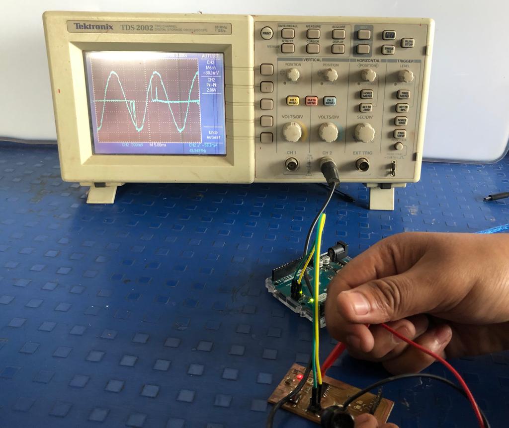
A.Group Assignment:We used the Oscilloscope in our lab to observe the operation of “Hello World” microcontroller circuit board.
B. Individual Assignment:I redrew the echo hello-world board with additonal button and LED with current-limiting resistor. Printed the circuit using SRM-20, soldered the components and tested it using Multimeter an Oscillator.
Group Assignment:
Jaydip and me teamed up to observe PCB on oscilloscope and multimeter.
Digital Storage Oscilloscope
An oscilloscope is commonly used to display and analyze the waveform of electronic signals. The digital storage oscilloscope is defined as the oscilloscope which stores and analysis the signal digitally, i.e. in the form of 1 or 0 preferably storing them as analogue signals. The digital oscilloscope takes an input signal, store them and then display it on the screen.
1. Volatge Curve: observing the voltage curves of the board. Good soldering should give rectangular curve, but the board had wavy lines instead. It could be because of some problem in soldering.
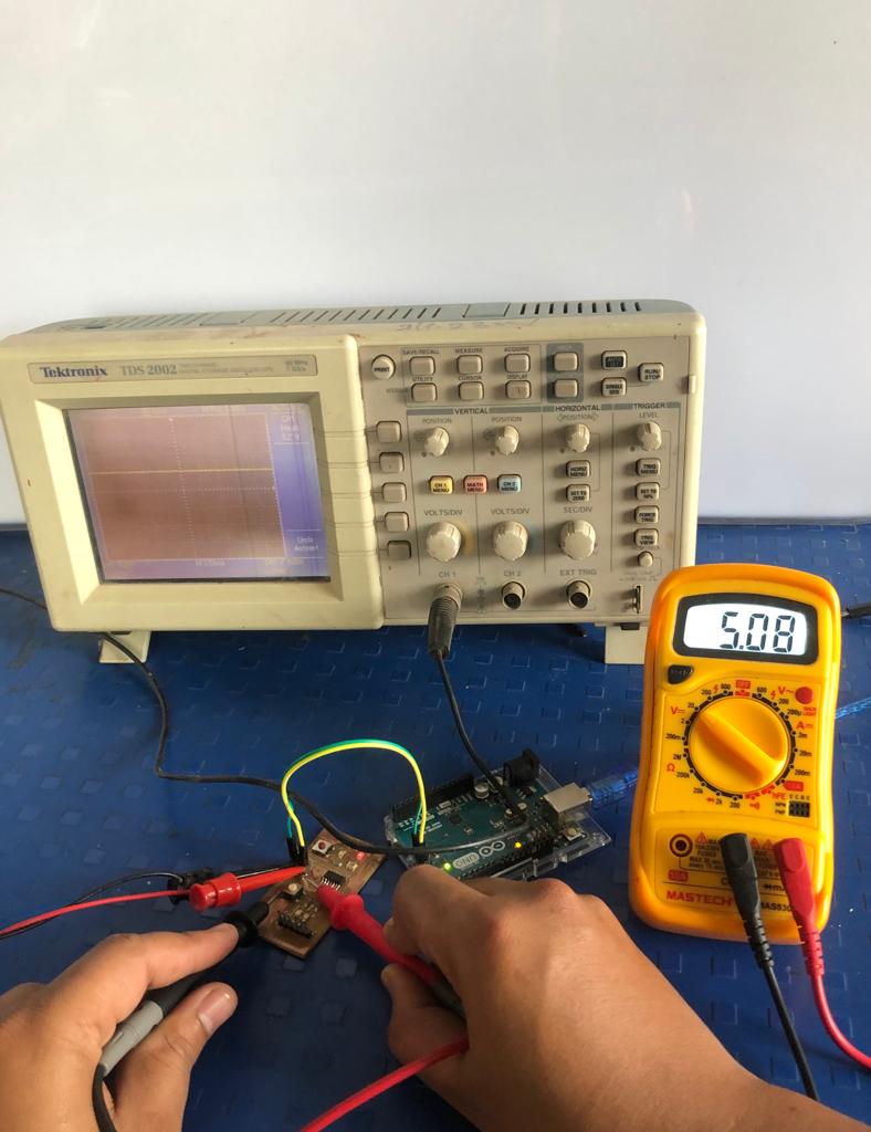
2. Voltage: Connected the board with Ground and VCC supply to observe 5V on oscilloscope. We confirmed it by oberving the same value on multimeter
Individual Assignment:
Design: I have used Eagle to design the board.
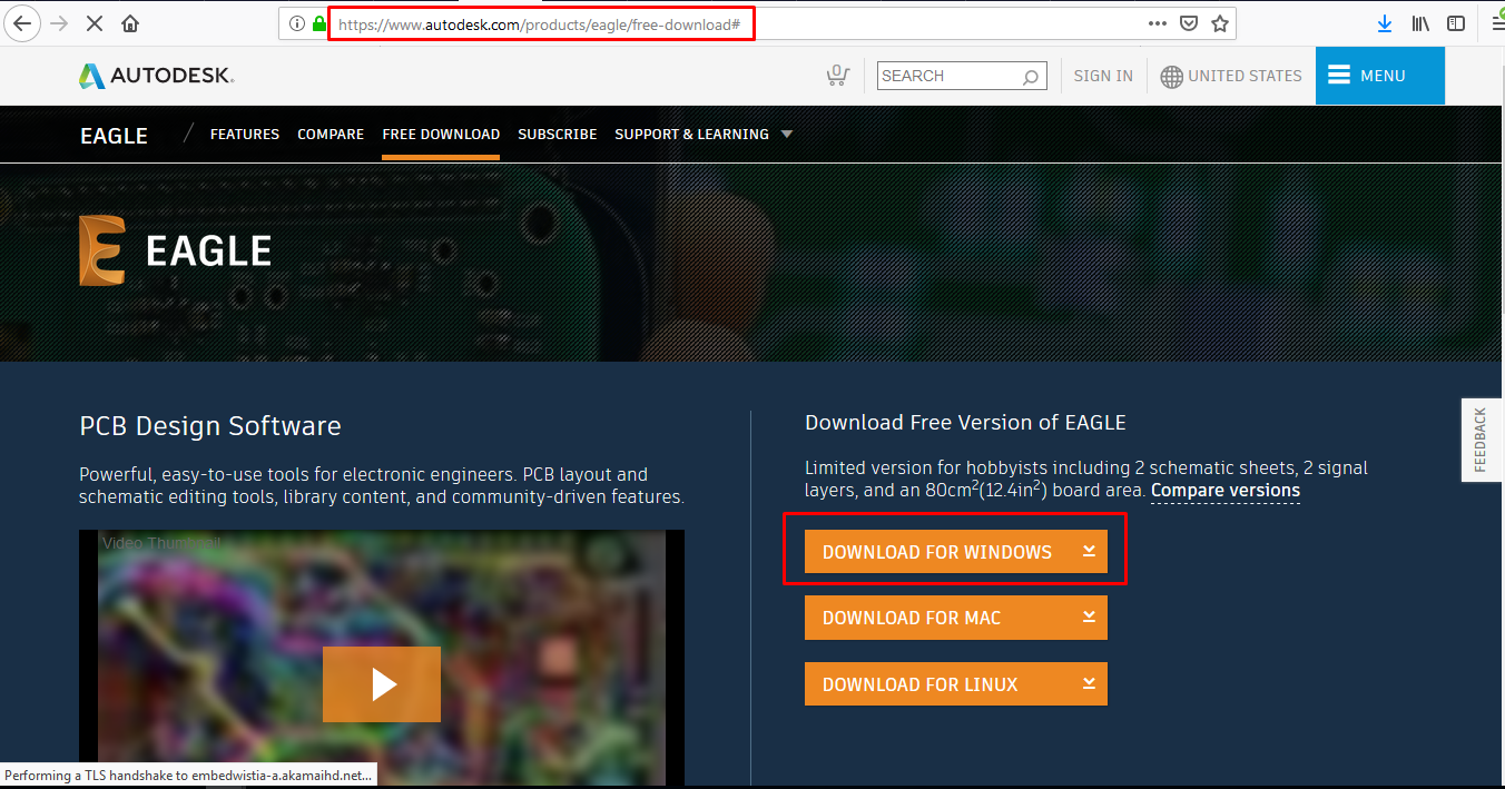
1. Downloaded Eagle:EAGLE (Easily Applicable Graphical Layout Editor) is a flexible and expandable EDA schematic capture, PCB layout, autorouter and CAM program. EAGLE is popular among hobbyists because of its freeware license and rich availability of component libraries on the web.
2. Installed Fab.lbr Library:
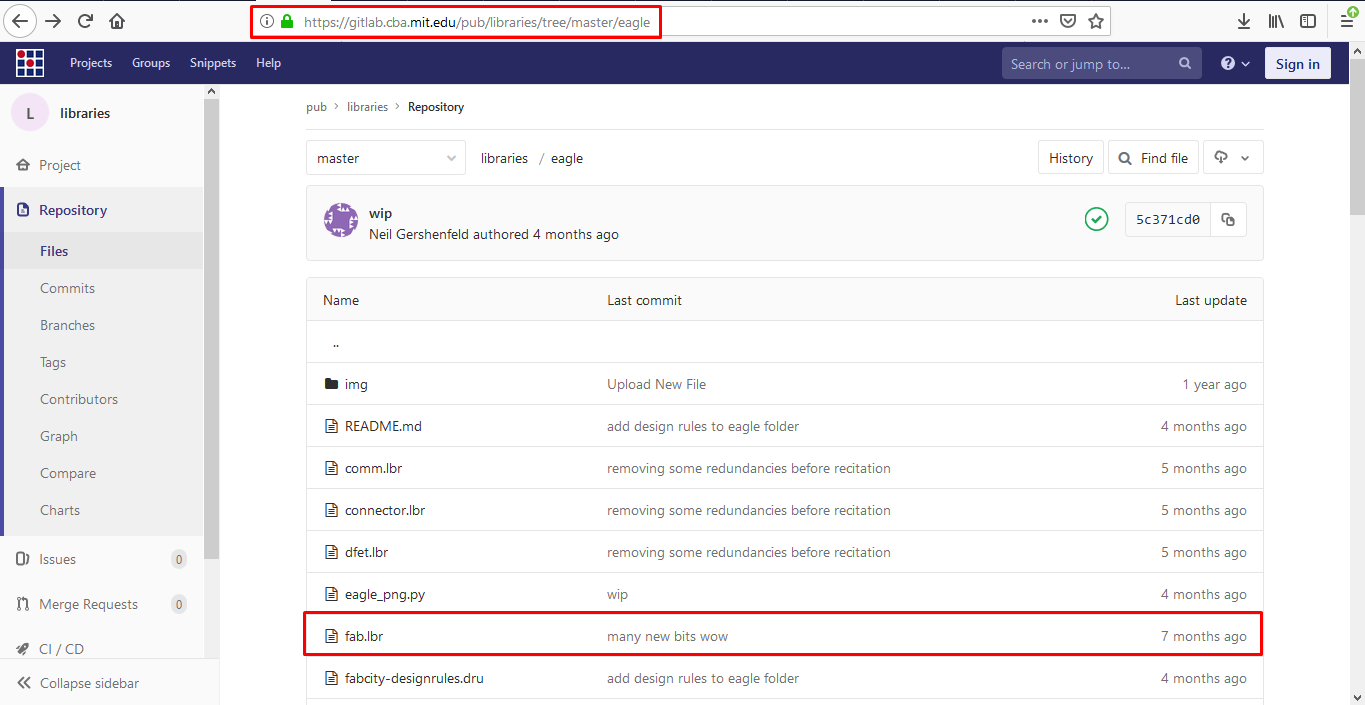
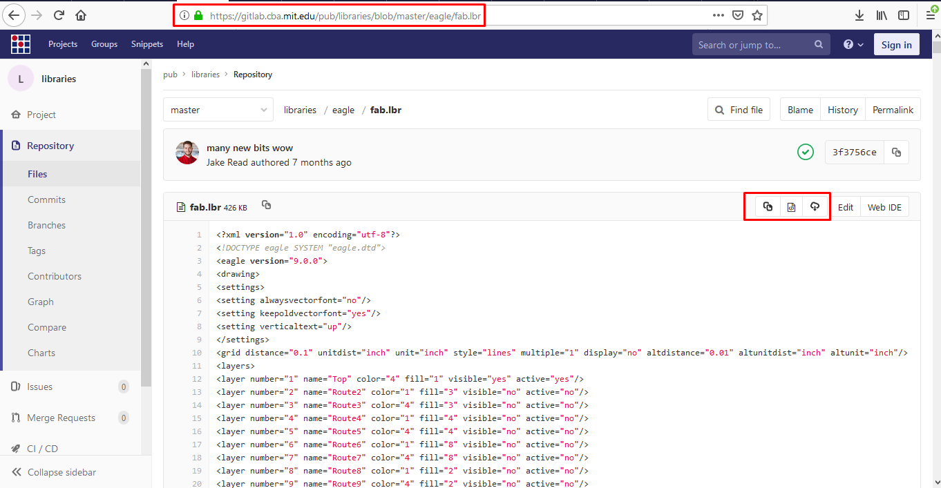
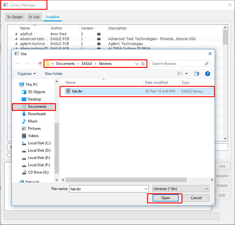
A. Downloaded Library: Git Lab gives access to a lot of libraries. I specifically downloaded fab.lbr for making “Hello World.”
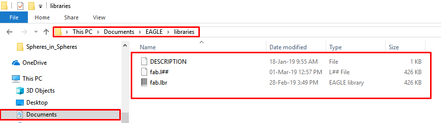
B. Library Location: This PC> DOcuments> EAGLE> Libraries. Moved the downloaded library to this folder.
C. Added Library: The downloaded library was added to the software.
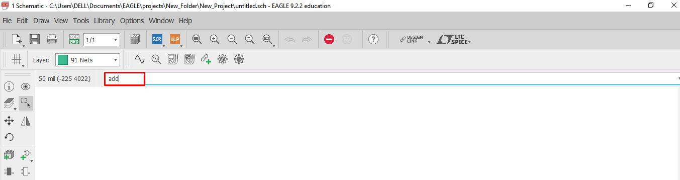
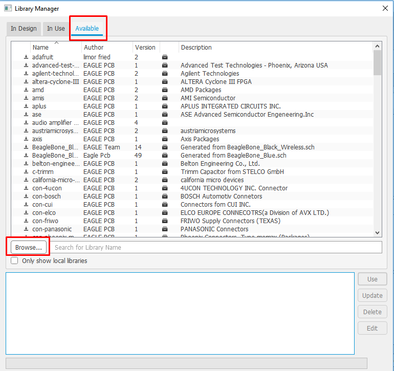
a. Command Line:“Add” gives access to the libraries to add components.
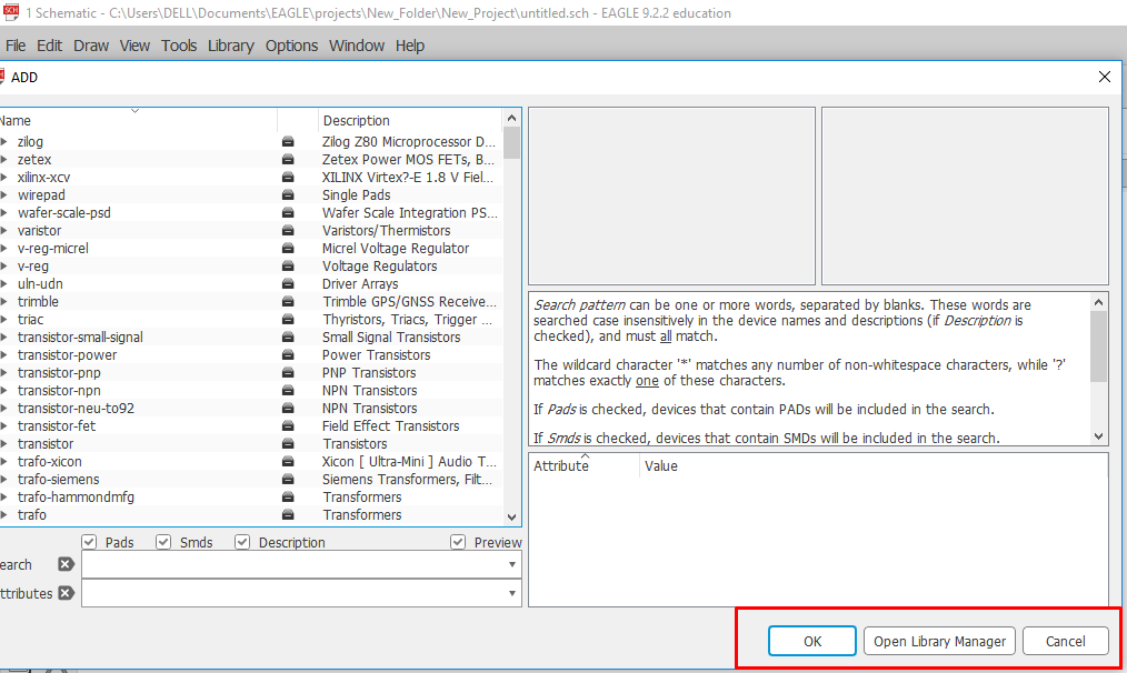
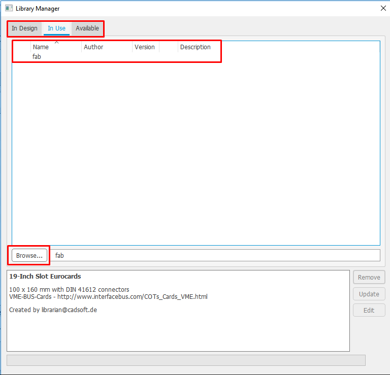
b.Library Manager:“Browsed” and selected the library fab.lbr liibrary from EAGLE libraries.”In Use” confirms the library has been added tp the software.
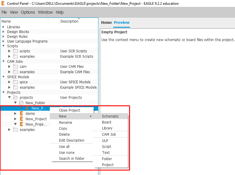
3.Created Project: On left side selected the option to add a new project and open the view to make a Schematic file.
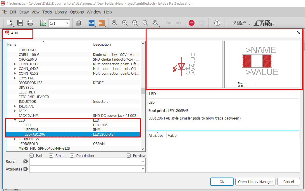
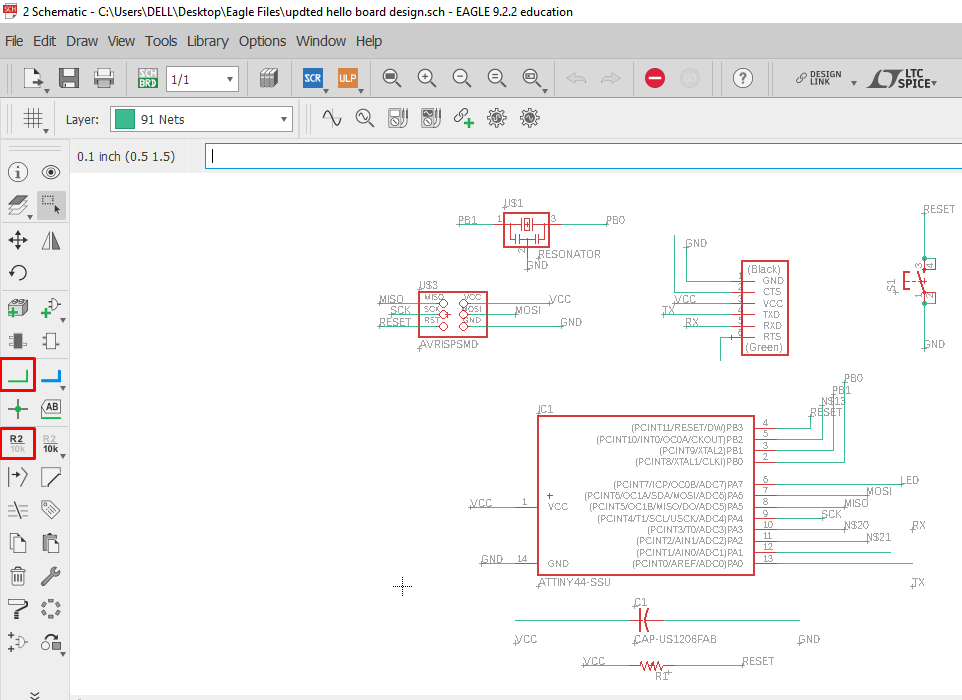
4.Schematic Design:A schematic in electronics is a drawing representing a circuit. It uses symbols to represent real-world electronic components. The most basic symbol is a simple conductor (traces), shown simply as a line. If wires connect in a diagram, they are shown with a dot at the intersection.
A.Selected Components:I chose components looking at Hello World Board and a few additional components.
a.Add: Typed “add” on command line which opened the library.
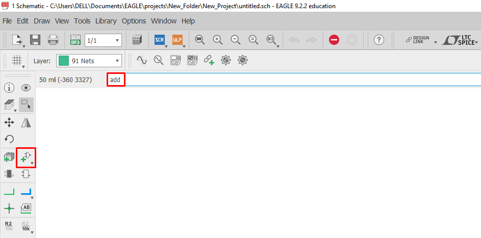 b.Library Components: This gave the option to add variety of the components. On the right side a picture of the selected component was visible. Added all the components.
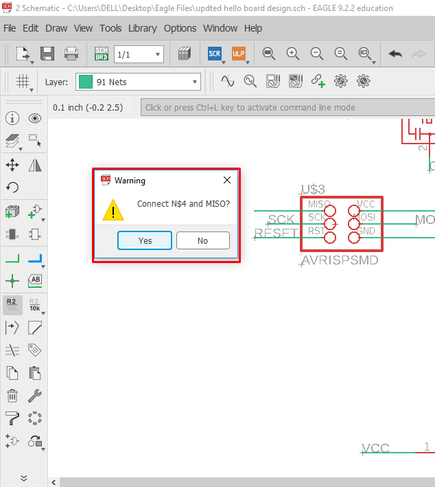
B.Made Connections:2 icons NET and NAME were used to label and connect the components.
a.NETS: Extended the connection using the tool in Green colour.
b.Name:Lablelled the end of the NETS. Parts with the same name got connected.
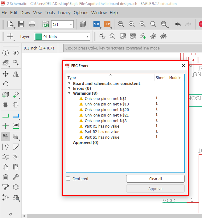
C. ERC Check:
There were no errors after ERC check and proceeded ahead.
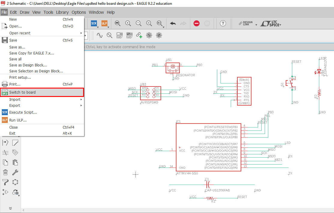
D.Schematic to board:Moved to the next step to make connections between the components on a actual PCB.
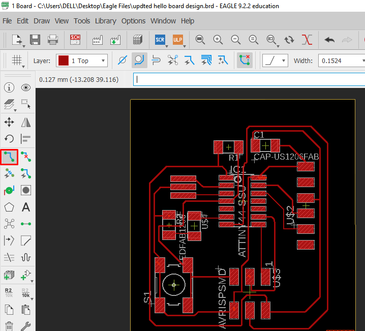
5. Board Design:On converting SCR to BRD button the actual PCB looked like the picture below which needs to be arranged and connected.
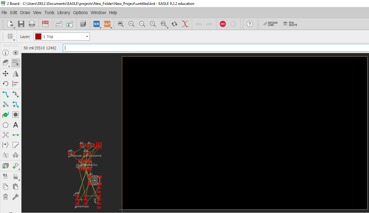
A.Moved Components: On left,using the “move” icon placed all the components on the actual PCB.

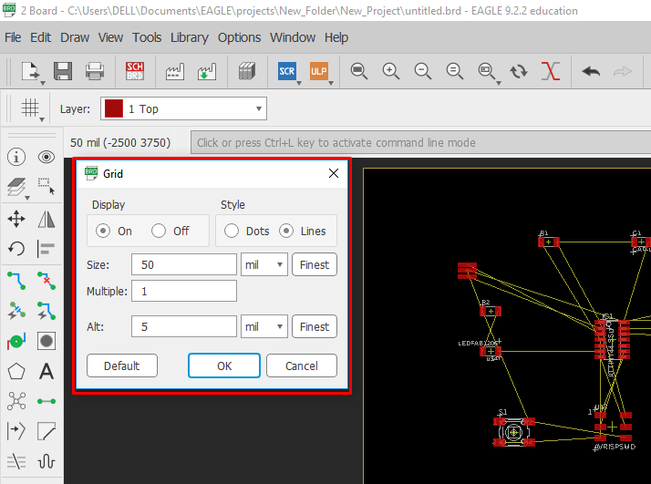
B.Grid:The squared boxes of the specific size helped in placing the route. I decreased the Grid size when precision was required.
C. Ratsnet: This tool connected the components at the shortest length of trace.
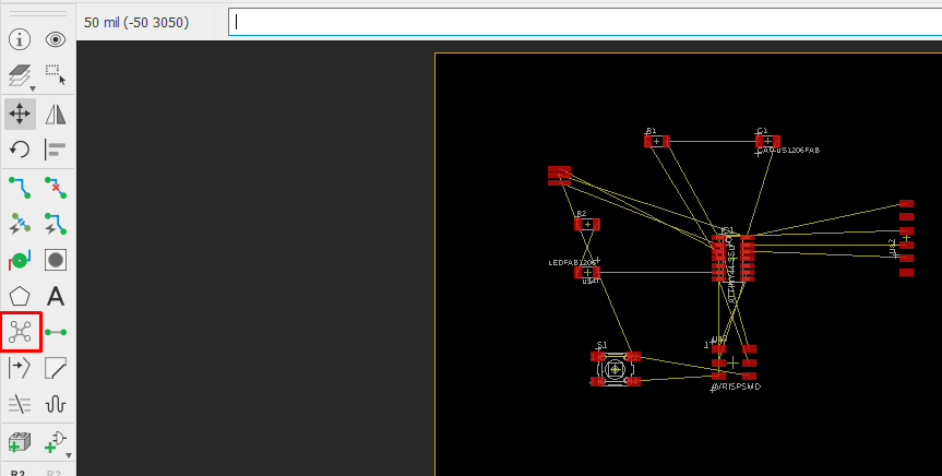
D. Route Traces: Routed all the paths which turned Red.
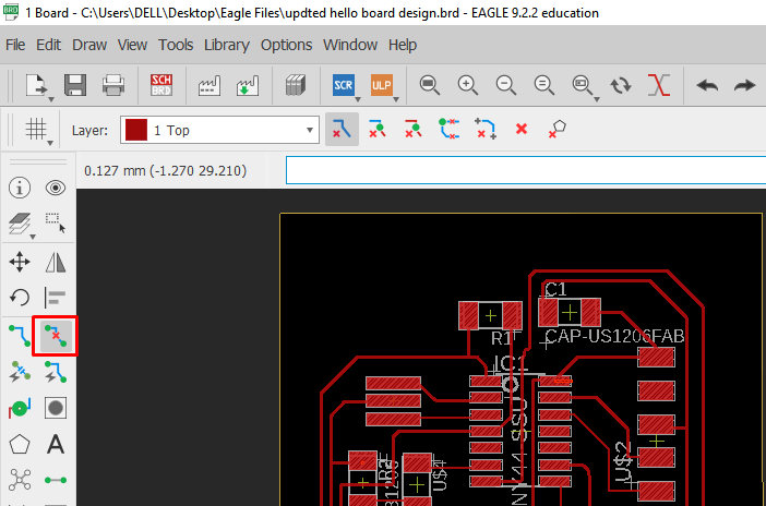
E. Ripup:Used the tool to delete the the route which turned the wire back to Yellow.
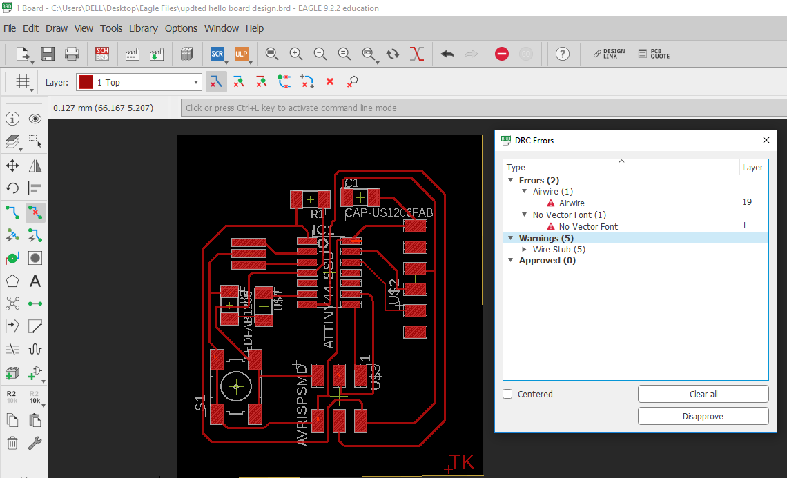
F.DRC Check:The errors were resolved which meant milling would be done properly.
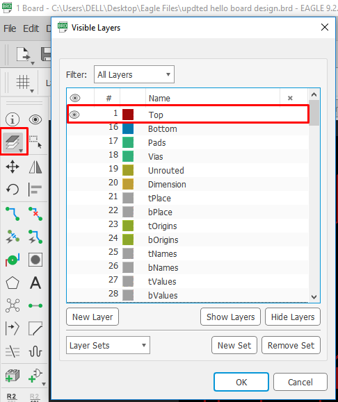
G.Layers: On keeping various layers on/off the details were added/removed. For engraving the file was exported keeping only Top layer on and for cutting keeping only dimension layer on.
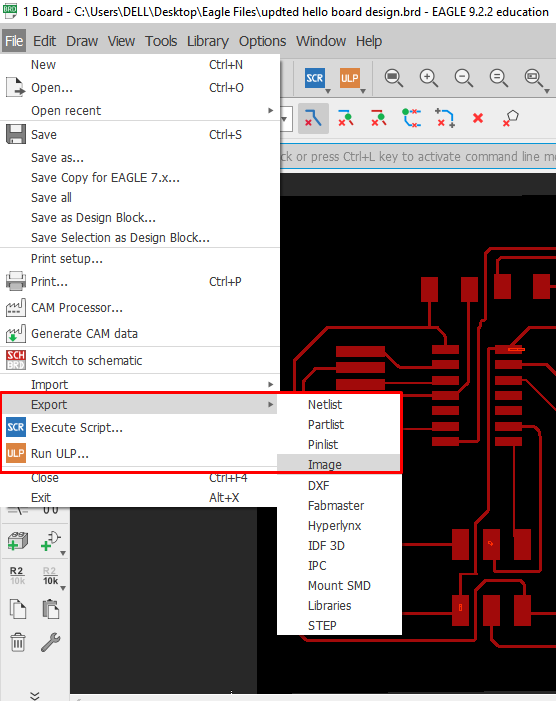
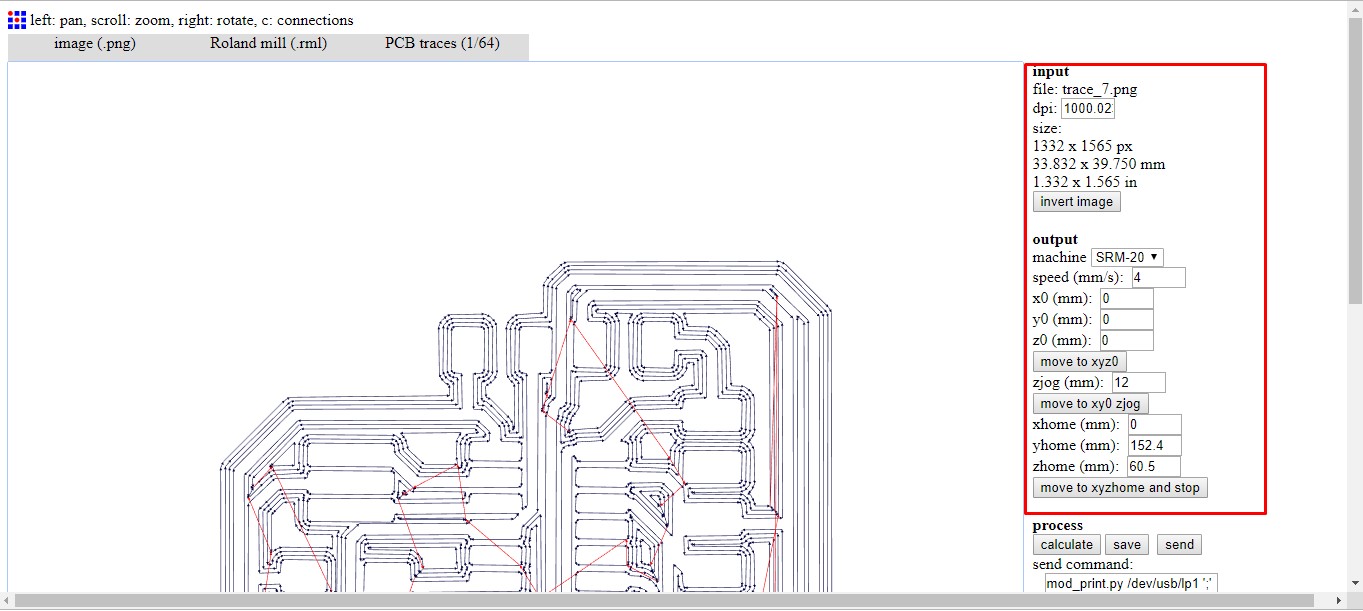
H.Export File: The files were saved in .png format.
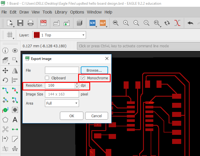
a.Monochrome: The machine SRM-20 cuts the Black and leave the White coloured design.It’s important to have the image in Black-White.
b. dpi:Adjusted the resolution to 1000 dpi.
I. Design Changes in Orignal board: I made the schematic and board by myself so routing or the design of traces is completely different. Moreover, I have added LED, a resistor to LED and a Switch which was not in the orignal design.
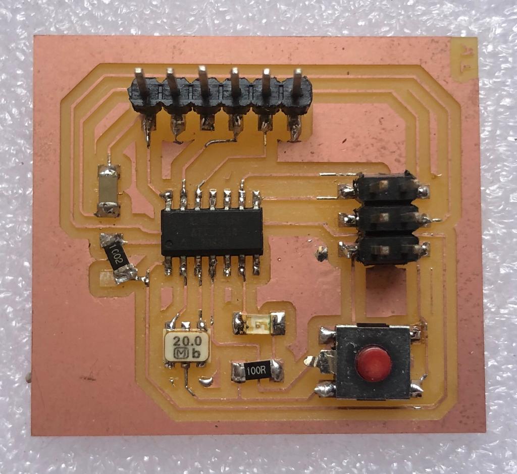
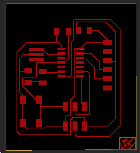
6.Final Board: The final board looked like-
Milling:
A.rml format: Using Fab modules(http://fabmodules.org/) converted the .png format files to .rml giving values of speed, x,y,z coordinates,name of machine, end mill size etc.
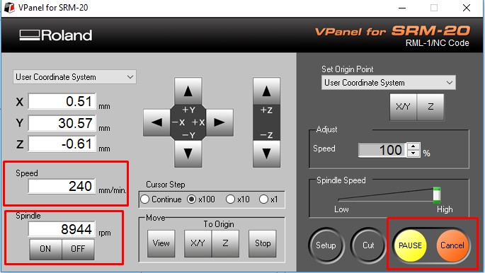
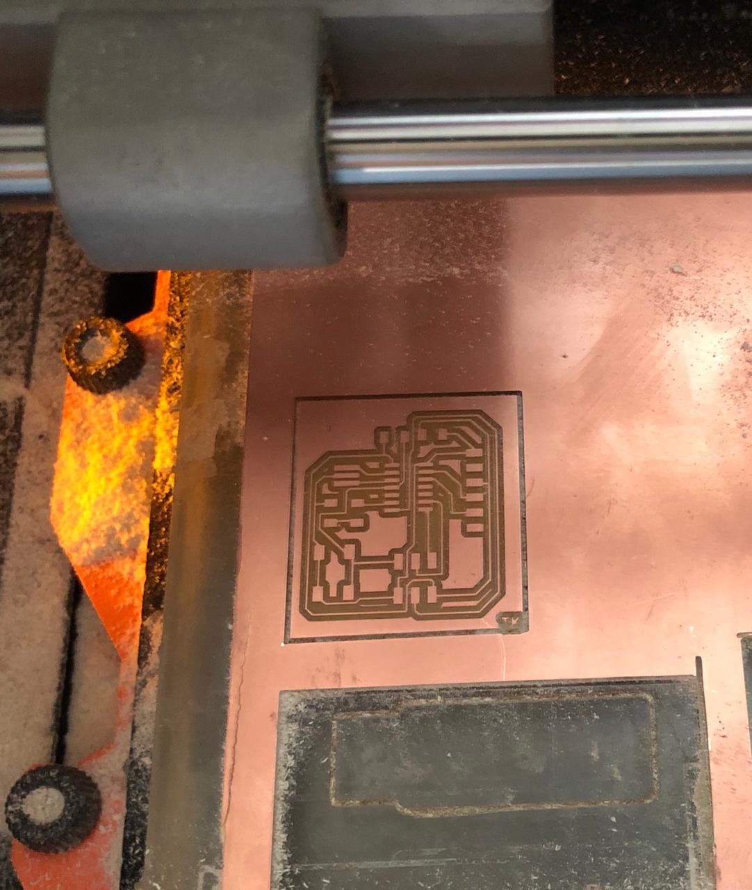
B.SRM-20: Using the end mill 1/64 for tracing and 1/32 for cutting milled the PCB. I used the software VPanel to instruct the machine.
Soldering:
A.Components:Following is the list of the components I soldered on PCB:
1. ISP
2. I.C.- Atiny 44
3. Resistor 1(R1)- 10k ohm
4. Resistor 2(R2)- 100 ohm
5. LED
6. Capacitor- 1 micro Farade
7. Switch
8. FTDI
9. Resonator-20 MHz
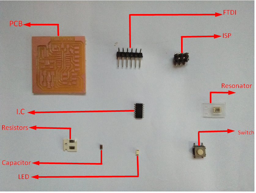 B. Fixing:Using filler, flux and the soldering rod placed and fixed all the components on the board.
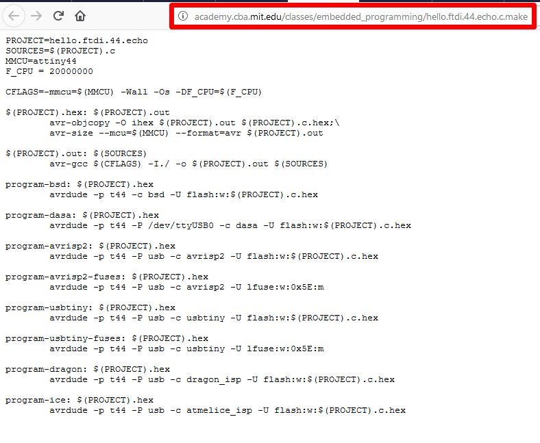
Programming: I referred the steps in the document
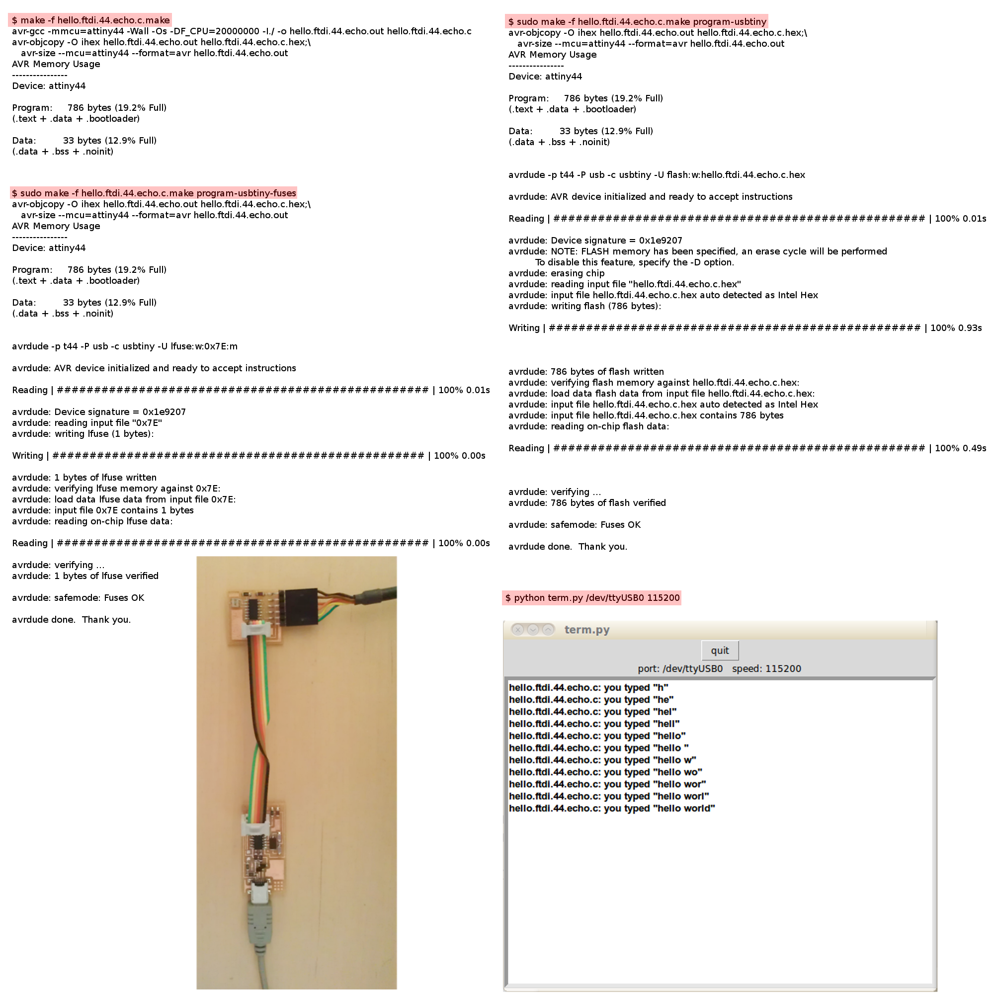
1. Step 1:
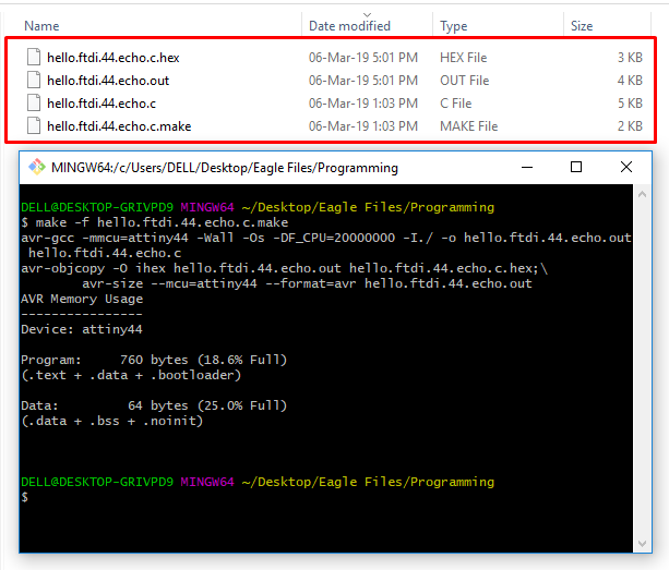
A. Downloaded “hello.ftdi.44.echo.c” and “hello.ftdi.44.echo.c.make” file.
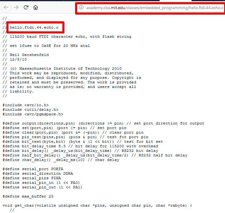
B. Saved “hello.ftdi.44.echo.c” and “hello.ftdi.44.echo.c.make” files in PC>Dekstop>Eagle files>Programming.
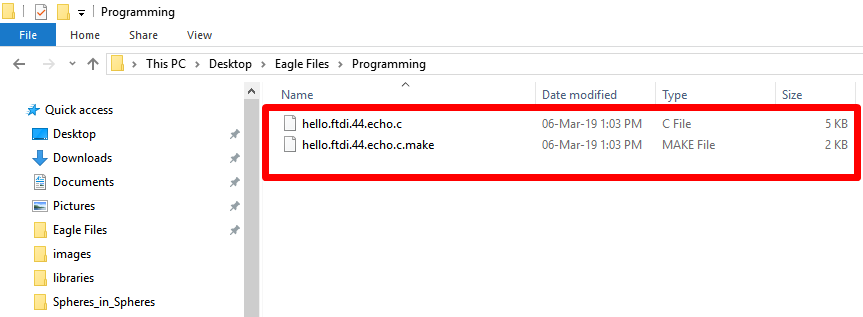
C. Hex File: 2 additional files HEX and OUT format were created in the same folder. This is basically the language in which the programme will be written onthe board.
2.Step 2:
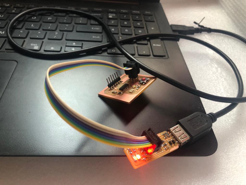
A. Connected board with ISP PCB:Using Ribbon Cable connected the ISP with my “Hello World” board.
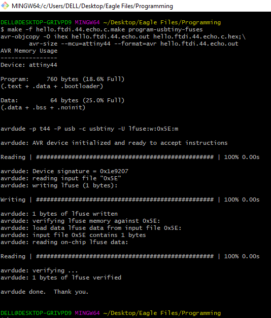
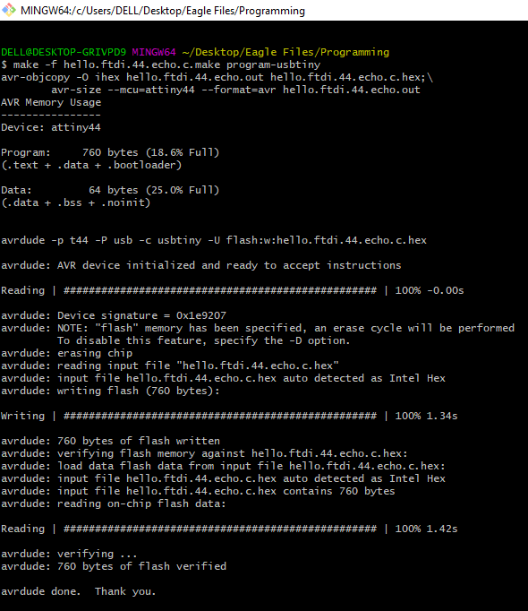
B.Run Command:On Gitbash using the command “make -f hello.ftdi.44.echo.c.make program-usbtiny-fuses” pushed the command and completed successfully.
3.Step 3:
A.Another Command:Keeping the ISP and “Hello Board” connected On Gitbash ran the command “make -f hello.ftdi.44.echo.c.make program-usbtiny.”
4.Step 4:
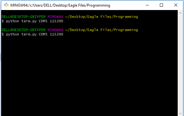
Gitbash as Administrator: Gave the command “python term.py COM5 115200”. This opened the python screen and successfully ran the programme.
Terms and Terminologies:
1. Photorsistor: also known as Light Dependent Resistance or LDR varies based on the incident light intensity. On blocking light on LDR the intensity of LED decreased and vice versa.
Application: On our phone we find a lack dot which checks the light intensity and accordingly adjusts the brightness of our mobile screen.
2. Diode: A diode is two terminal component, that conducts/allows current to flow in one direction. LED is also a diode which emits the light.
Application: Diode is used in solar panels where it doesnot allow the current to flow from the battery to the sola panel, thus avoiding the solar panel.
3. Reed Switch: It is an electrical switch operated by an applied magnetic field.If you bring magnet near the switch, the LED lights up.
Application:Reed switch can be used to check whether a door or a window is open or shut.Reed switch can activate the burglar alarm when soomeone tries to open a door/window forcefully.
Eagle design files available here.
Refernces
Fab Academy Tutorial
Mkdocs
Download Eagle
Fab.ibr Library
Hello World Board
Programming Steps