electronics productions
● I was really looking forward to this week from a while to gain knowledge and learn everything about printing boards, fabricating PCB, soldering the components, checking and doing several tests and to program using different softwares and drivers because i have never been introduced to this particular topic ever before. So it has been super interesting to work on the same with equally passionate students and helping each other out for this fun filled learning experience.
● My responsibility to complete the assignment was to print the board using the milling machine which was, solder the all the important components such as resistors, capacitors, mini usb, diodes etc, to do the board check through multimeter, smoke test, download essential softwares, drivers while following the recommended tutorials and then program it.
● Do visit the page for
DUBAI MINI MAKER FAIRE

getting strated
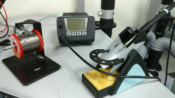
● I started my week by getting to know the milling machine, identifying the mill bits to be used and the software to operate the milling process on the machine.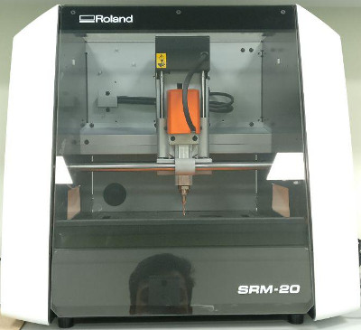 ROLAND SRM-20
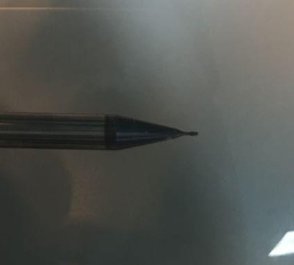
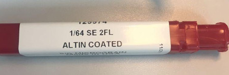
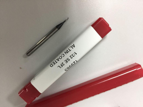 Identifying the 1/32 end mill for outline
 and 1/64 end mill bit for traces of the board.
● We downloaded the png file from HERE
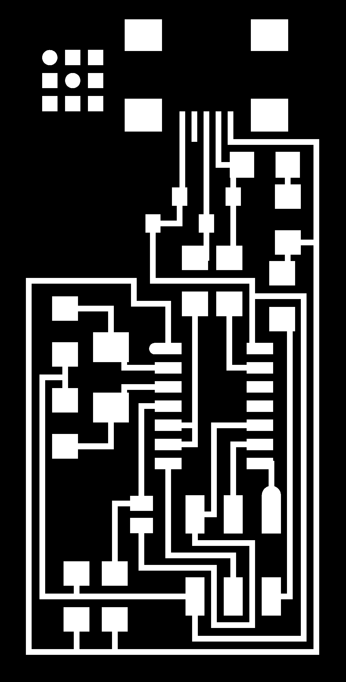
● Images of the interior as well the trace for the fab schedule page for the electronics production week to upload the same on the fabmodules.org website to specify correct parameters such as output format as RML, process involved to obtain the same on the machine software.
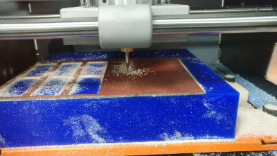
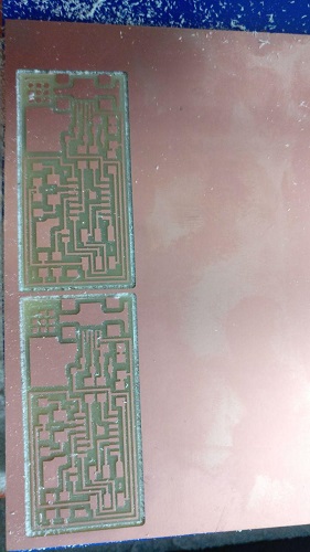
● First we start by fitting the 1/64 mill bit to cut the trace of the board, we set the z axis on the board by manually moving the z axis down towards the copper plate and then we let loose the mill and let it touch the plate thereby setting the z-axis. And for the x and y aix we set it as per the position and placement on the plate as per the size and space available.
● Once the traces are cut successfully we move ahead to cut the outline of the board using the 1/32 mill bit, we set the z axis for the the outline in the same way we followed the procedure for setting the z axis manually by moving the axis and letting it loose and just touch the board thereby setting the z origin
● We used copper FR1 material to be printed and traced on, also using a double sided tape to ensure the placement and for better outcome.
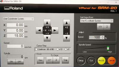
● After that we opened up the VPanel application to set the x,y and z axis in order to notify the machine to carry out the milling at the specified area on the Copper FR1 material.
● We made changes only in the user coordinate system on the VPanel which resulted in the expected change in the machine coordinate system.
● We initiated the process by printing the trace file using the 1/64 end mill and moving on to printing the interior outline with the help of 1/32 end mill, also adjusting the z axis before starting the print for respective files in order to obtain the perfect z axis height. We used 2 types of end mill for our assignment as specified by our instructor.
● The printing process was done successfully and I was amazed to learn the new machine and software to print boards.
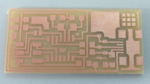
● Once the printed board was ready I cleaned the board softly by using some soap water and making sure the surface is tidy to solder on.
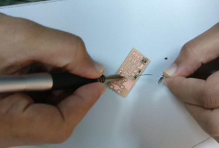
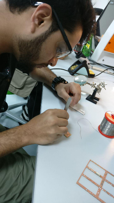
● Moving on the next step of the assignment and the most intense in my personal experience was to solder the important electrical components on the board.
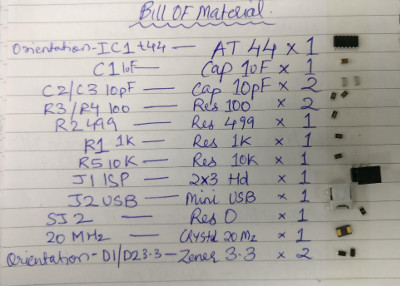
● I started on following the tutorial using the images of the board and components in order to verify each step and part. I made a list of the materials with respective codes in order to ensure not losing the microscopic stuff and for better understanding. It was a very helpful step decided by the group to make a bill of material by using a double sided tape for learning progress.
● I did practice soldering before I made use of the components such as resistors which resists the power on the board, capacitors to store the power, crystal to manage the time, mini usb for connection of programming, jumpers for connection, IC circuit for power,J1 ISP is the 6 pin programming header and zener diodes which at a critical reverse voltage a large reverse current can flow.
● Soldering each of them in a particular pattern to not disturb the progressive process was the goal. It needed utmost concentration and minimum coffee to do the same. I started off with soldering the big components first in order to avoid any disturbance on board to solder the small components. I also made sure to check the connections as I soldered and also kept in mind to apply the technique of soldering the components in one area and move on to the next area.
● Once done with the soldering process, I realized that the the Attiny44 was connected in the wrong direction and so I had to make a new board and follow all the steps again.
● I had to mill a new board a program it as:
I connected the attiny44 in the wrong direction resulting in a failed connection.
● I took this mistake very positively in order to learn more and felt lucky in terms of practicing once again the soldering process and the programming process. In total I milled 2 boards for this week and the latter one was programmed correctly as it had all the right connections.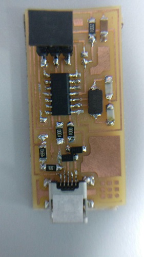
● It was a very important practice to check the soldering connections while doing it ensure it works, we used the multimeter to check the connections once the entire board was soldered with the above mentioned components.
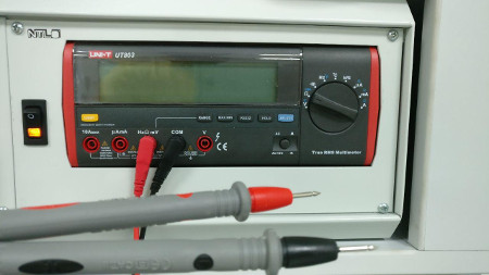 MULTIMETER
● Also check out WEEK 07 where I used the Multimeter again to test the board I designed for Electronics Design.
● We used the above shown multimeter to test the connections by putting it into the manual mode and using the Volts (sound) ohm option available. So as per the connection the multimeter made a typical sound which shows there is a connection between two traces or the components. This ensures that there is a connection or if there is a failed connection if it makes no sound or also if it makes a sound where there has to be no connection.
● It was a very important practice to check the soldering connections while doing it ensure it works, we used the multimeter to check the connections once the entire board was soldered with the above mentioned components.
● I was regularly following the tutorial images for much better learning progress and to make sure that everything is done as per requirement. I checked each and every connection twice being my first time getting to know the essentials of electronics production.
It's been a great challenge to program a board for the first time in my life !!!
● So basically once the board is ready, I used a Mini usb cable to connect the board tpo my laptop and to smell the board and do the smoke test. I observed no smoke coming out of my board which meant that my board passed the smoke test and everything is soldered properly. It is highly recommended to do the smoke test before starting to program the board. Otherwise it would harm the laptop and something might get damaged.
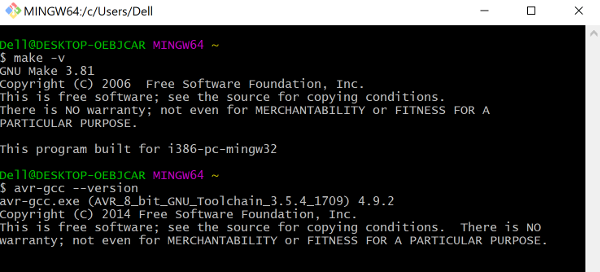
● After the smoke test we start downloading the softwares, installing the same and also installing the particular drivers to identify the FABISP.
● I downloaded Atmel Gnu toolchain, GNU make, AVRdude, fabisp firmware file, the driver for windows and the zadig software used to re install a driver from a programmed board to the one which has to be programmed. I had to check the correctly installed software through git bash.
● I also changes the environmental variables of the advanced system settings, edit the path and new path for avr dude, gnu make , and gnu toolchain.
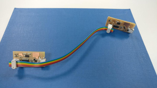
● We had to connect the programmed board to the board to be programmed through the cable shown in the picture and then follow the steps as mentioned in the tutorial.
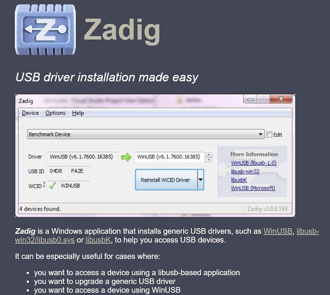
● We used Zadig software to install the generic USB driver, as explained in the above picture. Also here is the LINK to download zadig

● Then I edit the makefile as per instructions in order to proceed with the programming commands.
● Then the following commands were used in the git bash terminal were the firmware make file was extracted. make clean
make hex
make fuse
make program
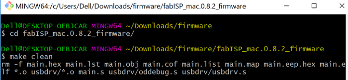
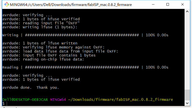
Successfully programmed the board through the instructions provided and the commands for git terminal.
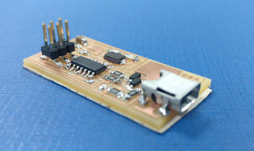
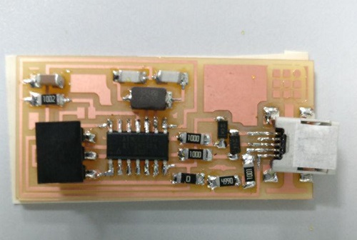
We see the Programmed ready Board
Links & resources
Highly recommend to follow the below links for better understanding for this week
Tutorial link for Making the board
Link for Downloading AVR TOOLchain
LInk for AVRDUDE
Link for Tutorial from Fab Academy page
Link for Demystifying the FabISP
● I used my own FABISP for the folowing weeks to program several PCB's.
WEEK 09
WEEK 11
WEEK 12
learning outcomes
● Apart from the electronics production we did some exciting stuff for our lab.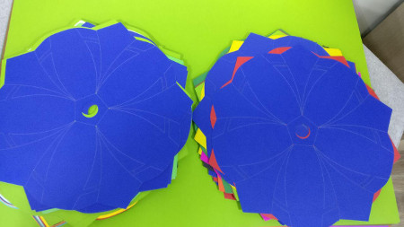
● Our instructor prof. Wendy gave us the opportunity to help a great deal in order to participate in the maker faire in one way by creating lampshades out of color full cardboard on the laser cutter machine. It was amazing to know the different process for such a design and we enjoyed folding the lamps.
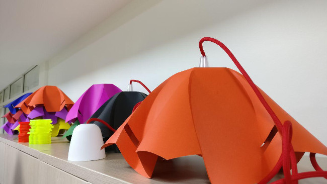
● Really looking forward to the maker faire starting in a day.
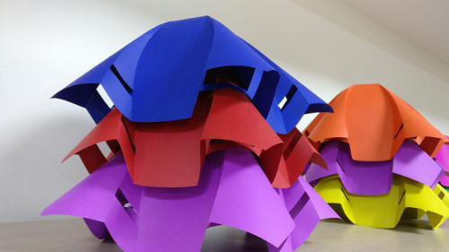
● These lampshades will be used to showcase on of the weeks of fab academy and express the same, also people attending the faire would be able to make some lamps and carry them as a souvenir.
● I learned that a printed circuit board (PCB) mechanically supports and electrically connects electronic components or electrical components using conductive tracks, pads and other features etched from one or more sheet layers of copper laminated onto and/or between sheet layers of a non-conductive substrate.
● WIll be using my programmed board in the coming weeks for anything such as from smartphones to kitchen appliances, electronics play a large part in our daily routine. At the heart of each of electronics is a printed circuit board (PCB). It is the foundation of a majority of electronic products today.
●
These components come in a vast array of configurations, allowing them to serve a variety of functions. As electronics expand and develop across industries, PCB applications continue to grow as well. Today, the use of PCBs spans just about every industry and continues to evolve into new industries and applications. PCBs are the major functional centers of most electronics in the modern world. Circuit boards connect components to one another through a series of related circuits - from Wikipedia