getting started
● We started the week with a very informative lecture on Electronics Design topic by Neil, which was very new for me and personally it gave me a good understanding about the software part, all the components involved in stuffing the board● Wendy introduced us to KICAD, also mentioned the support kicad receives from The European Organization for Nuclear Research (French: Organisation européenne pour la recherche nucléaire), known as CERN. Which is indeed quite interesting.
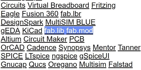
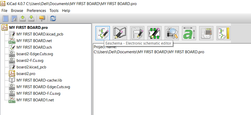
● I chose the very user friendly software and easy to understand for starters, Kicad, to design my board with the LED and the Button, first step was to start with a new project on KICAD and add the fab library from the preferences so that we can add all the components in the fab inventory for electronics design.
● Download the library from Fab Academy schedule page HERE
● Keeping in reference the Neil's board, I had to just add a Resistor, LED and a Button to a PCB designed by me, mill it and solder the components to test it.
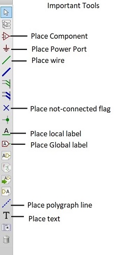
● Starting to identify the essential tools in the software in order to make the schematic, place wires, labels and also using the important tools for checking them.
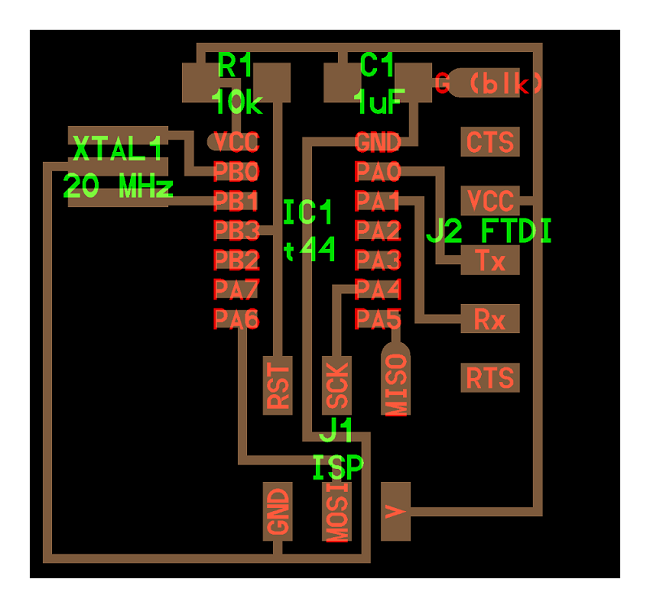
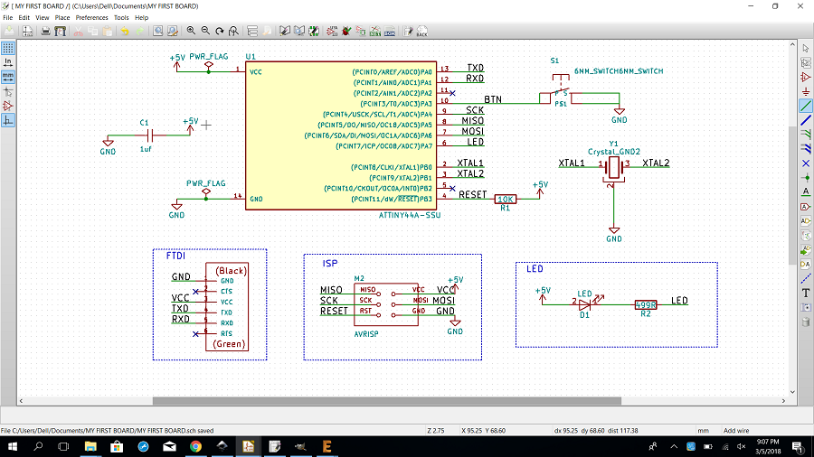
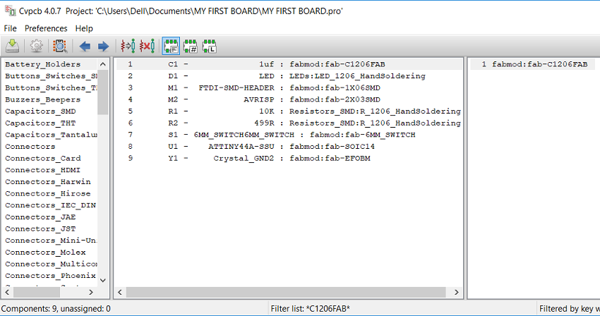
●The next step was to place the components one by one and the following components were selected:
● I found thr below description of each components from Google, to get a better understanding of the application and function for each one of them.
● ATTINY 44
- Microcontroller, is a control device (the brain) which incorporates a microprocessor.● FTDI
- Future Technology Devices International, This is a USB to TTL serial cable, with a FTDI FT232RL usb/serial chip embedded in the head. It has a 6-pin socket at the end with 5V power and ground, as well as RX, TX, RTS and CTS at 3V logic levels.● AVR ISP
- 2x3 Header which enables a user to programme the PCB by connecting it to the other ISP (FABISP) in this case. Used for programming, data, power, or any other kind of connection.● Crystal
- Generally used in timing, sensitive circuits.● Capacitor (1uf)
- Its function is to store the electrical energy and give this energy again to the circuit when necessary, it charges and discharges the electric charge stored in it. It blocks the flow of DC and permits the flow of AC.● Resistor 1 (10k)
- Are used to reduce current flow, adjust signal levels, to divide voltages, bias active elements, and terminate transmission lines, among other uses.● Resistor 2 (499R)
- Basically used for a protective purpose to resist/reduce the current flowing to the LED, also to avoid the LED from burning due to high voltage current.- I used this particular resistor based on the calculation of Ohm's law formula which we calculated during a session with Hashim as shown below.
Ohm's Law is given by: V = I R
where V is the potential difference between two points which include a resistance R. I is the current flowing through the resistance.
- Based on the above formula and the Datasheet of the Blue LED which has been used for the accurate information regarding voltage and current, I calculated that if
Voltage (V)is 5 Volts and Current (I) is 40 Miliampere (i.e 0.04 Ampere) so the resistance (R) is the Voltage divided by the current as shown below:
R = V/I
= 5 / 0.04
R = 125 ohm
- The calculation as per the formula explains I need at least 125 ohm resistance and so accordingly I select the closest resistor available -499R for the above mentioned function and purpose.
● LED
- Light emitting diode that shines if it gets at least a minimum voltage.● Button / Switch
- Button with the "push-to-make" (normally-open or NO) mechanism are a type of push button electrical switch that operates by the switch making contact with the electronic system when the button is pressed and breaks the current process when the button is released.the schematic with ALL THE COMPONENTS
● We choose the tools below in the order of their placement which was a very helpful way to understand the making, associating and checking process of the design schematic for my board.
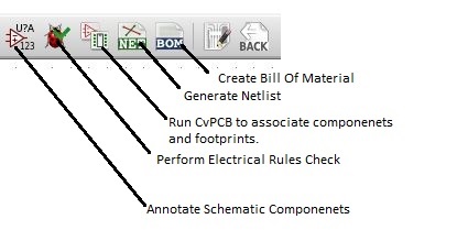
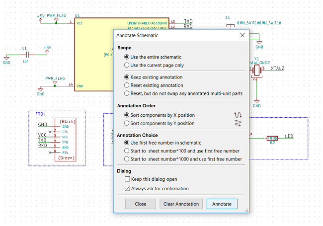
● Accordingly we name and label the components in the way they will be connected to each other and while we place the components we also use the annotate tool to check the annotation of the same.
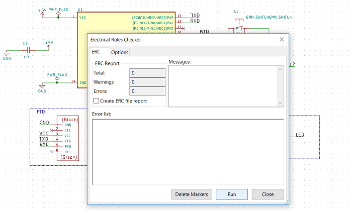
● Moving on we do an electric rules check using the tool next to annotate tool on in order to check all the connections done correctly while labeling and placing the components.
● Next step is the association for all the components we chose, with the fab library to ensure the same components to be used for soldering on the board.
● Accordingly we associate each the component with itself from the library and move ahead.
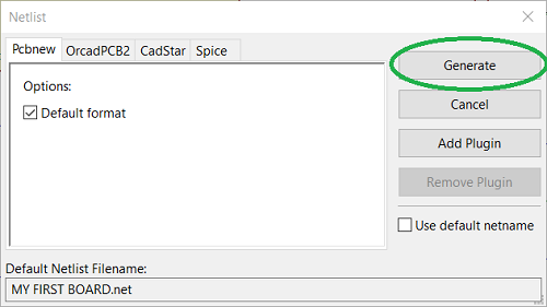
● Then we create a netlist in the default format as a Pcbnew to generate the same.
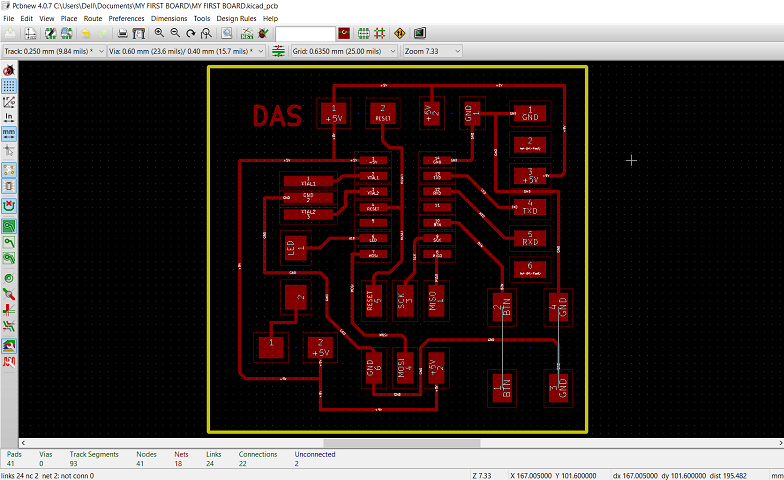
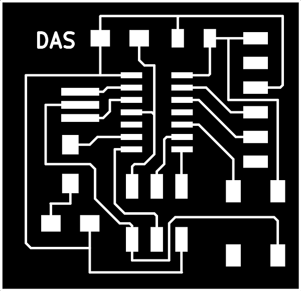
● According to the connections I made the traces for all those connections and made sure that no trace crossed the other one, this entire process of designing a pcb board was very new for me and I literally enjoyed each and every bit of it in order to learn more.
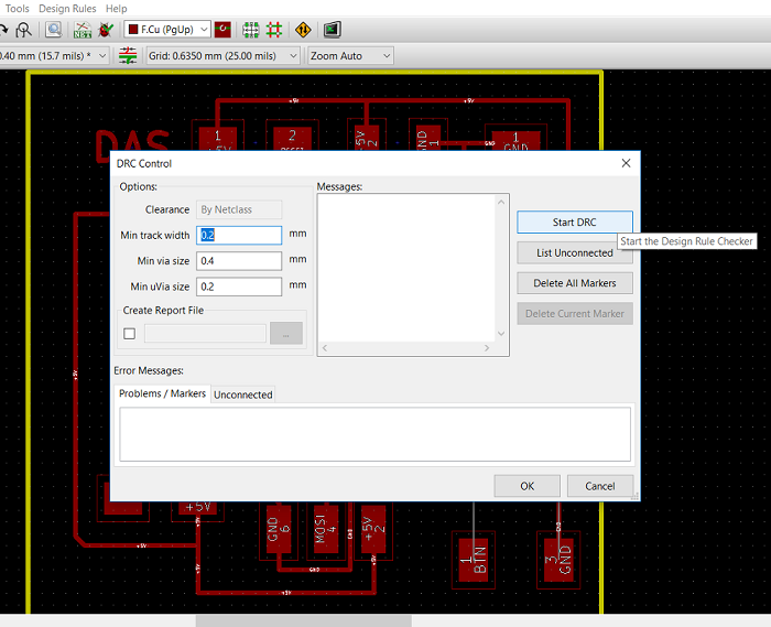
● We also perform a design rules check and select the Min track width 0.2 mm in my case and the min via size etc. at 0.4 mm. Once the rules check is successfully completed we move on.
● So the designed board was ready to be saved in two seperate file, 1 for trace and 2 for the outline.
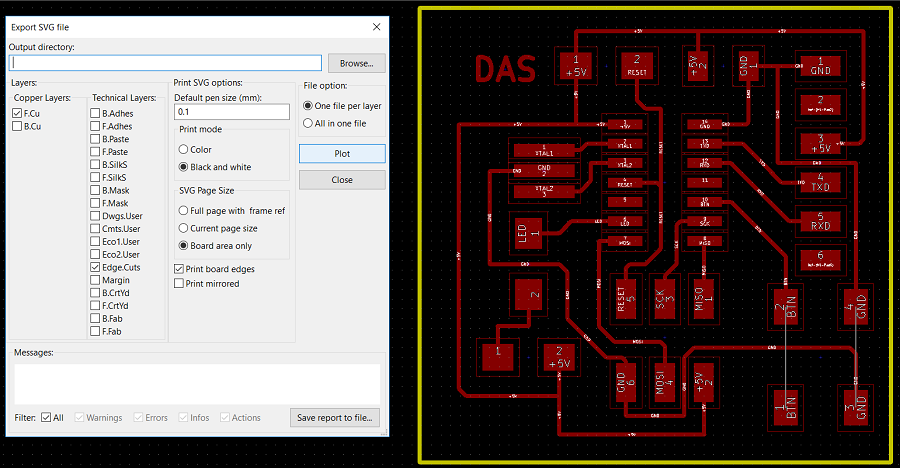
● We export the file in the form of (.svg) from the kicad software and just select the edge cut layers to achieve what we want.
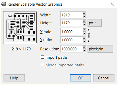
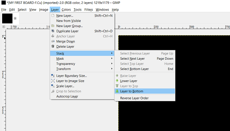
● Then we import the same file in GIMP and keep the ratio same but we modify the resolution to 1000 pixels per inch.
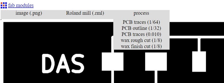
● As we have to save in the format of.png in order for it to be recognized by the fab modules so that we can download the (.rml) file for cutting process.
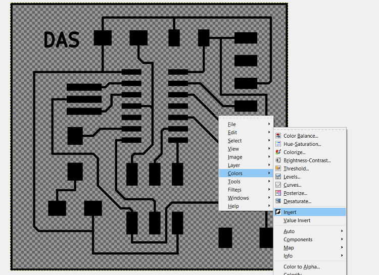
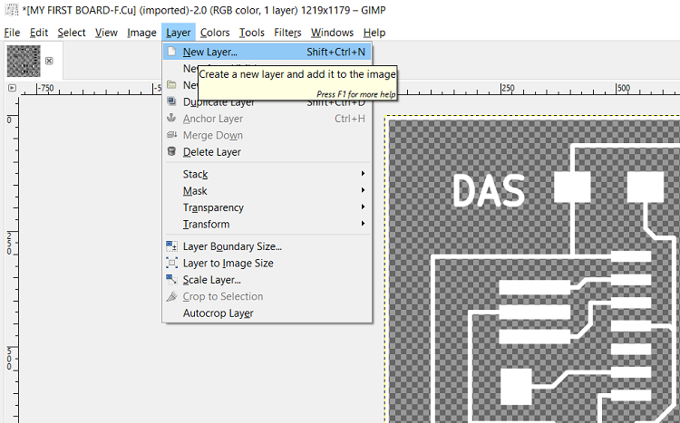
● First we invert the color of the image from black to white and then we add a new layer to the image and with black background so the visible image in front of turns entirely black, then using the the option from layer/stack we choose layer to bottom so the new added layer goes to the bottom and we have the requires image in front of us.
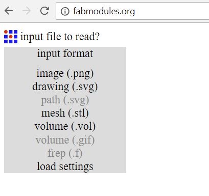
● We save the trace and the outline that we created on GIMP and then we upload the same on fab modules and we select the options accordingly.
● We import the (.png) file as given in the options to upload in the input format as image on the website.
● Then we select the output format as (.rml) so as to save it and then the to cut the file on Roland Milling Machine.
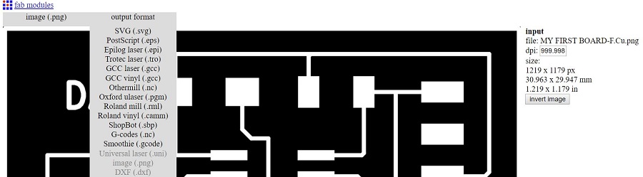
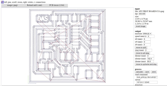
● We also have to select the process as 1/64 traces as we will be using the 1/64 mill bit to cut only the PCB traces of the board.
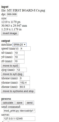
● Then we have to select the machine as per the model no. at the lab, for us it was SRM-20 and then we calculate the machine cutting process to ensure that the cutting looks alright and then we save the (.rml) file
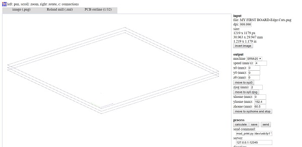
● We follow the same process to upload the (.png) image of the outline and choose (.rml) as the output format and the only change is to choose the process 1/32 for the PCB outline traces for the same. We select the machine, calculate the cutting tool path and save the (.rml) file.
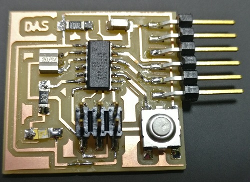
● The next step was to make the bill of materials as shown in the earlier image and start soldering.
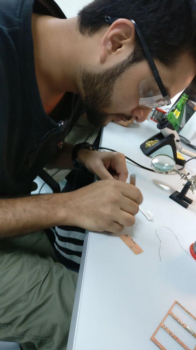
● This time the soldering process was comparatively easier for me as we practices a bit and we know how to go about.
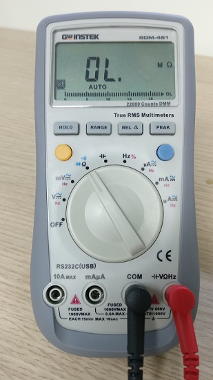
the button and led board is ready to be tested using
multimeter
● Next step is to test the connections on the Board using a Multimeter, as shown below are also known as a VOM (volt-ohm-milliammeter), is an electronic measuring instrument that combines several measurement functions in one unit. A typical multimeter can measure voltage, current and resistance. We generally used it in the manual mode for continuity test as explained below.
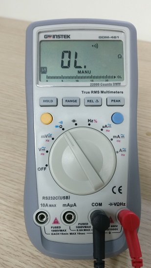
interesting stuff here
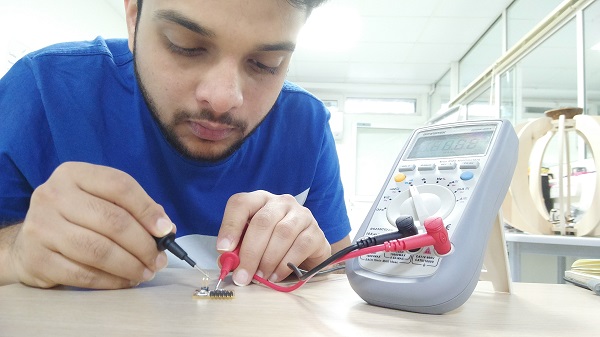
● In this case I am using a digital Multimeter only for the purpose of testing with the help of continuity mode which means: If the probes are connected—either by a continuous circuit, or by touching each other directly—the test current flows through. The screen displays a value of zero (or near zero), and the multimeter beeps. Continuity! If the test current isn't detected, it means there's no continuity. We use the VCC (red cable) and GND (black cable). This is indeed a very important aspect of the overall process of making a circuit board.
my designed pcb is ready :)
do check out the oscilloscope Session
& how i Programmed the board in
WEEK 09
learning outcomes
● Download the schematic and board file for kicad HERE
● Download the (.svg) files for the the board HERE
● Download the (.png) files for the outline and traces: HERE
● I learned how to use KICAD and design PCB board while using the fab libraries and how to associate those components, while performing multiple checks for design and electricals.
● I also learned how to use to image editing software, to convert (.svg) images to (.png) images with the specified color combination. And upload the same on fab modules and download the (.rml) file for cutting the PCB on the Roland SRM-20 machine.
● And had a better understanding now of using the vpanel software for the milling process, while setting the x,y and z axis and also changing the mill bit for traces and outline cutting.
● Soldering is much easier now I can say, plus I am getting a better idea of identifying the components and their applications.
● It was a very valuable week in terms of the range of topics we covered in mere 4-5 days and implementing all of that was one of its kind opportunity for me again.
● The testing part of the PCB, using a multimeter and getting to know the oscilloscope was very new for me and I enjoyed every bit of it.