Week 11
Getting started with Input Devices
This weeks assignment was to get started with Input devices and add some sensor to a Microcontroller board and program it.......
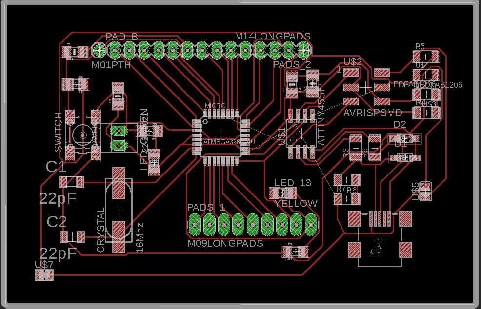
This week I decided to create a board which would be used furthur in my final project ........ Lets create a board around ATMEGA 328P ...... I went through a lot of pages and while going through pages I came across SATASHA KIT ..... But in this kit I observed some problem..... It has to be programmed exteernally using ISP programmer ....... So I decided to improve the design and Incorporate Programmer within the same board..... Well this seemed to be an easy task ....... but actually it wasn't ...... I downloaded SATASHA KIT Board files and then modified its schematic.....
Getting started with SATASHA KIT
SATASHA Kit was an imroved version of FABKIT ...... as it was much cheaper and involves components which are easily available ...... I started tearing it off and adding Programmer to the main board ......
For adding programmer I decided to add FABISP programmer and this is how I interfaced both the boards ......
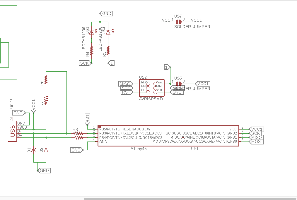
Points which I have considered while Interfacing
1. I considered that while programming ATTINY 45 only it has to be powered up.... other which ISP may get confused which one to program..... So I placed a solder jumper between power supply track of both the controllers.
2. Similarly MISO, MOSI and RST Lines need to be isolated while programming ..... So I decided not to route them ...... and connect them externally using jumper wires.
3. I added extra filtering caps
Its time to get the Board Printed
The first step is to convert Board Layout to Image (.png file)
This procedure has been documented in week 7 i.e Electronic Design week (LINK)
The second step is to convert .png file to .rml file using Fabmodules
This procedure has been documented in week 5 i.e Electronic Production (LINK)
I was a bit worried about the tracks as they were only 10 mils but, after proper setting and tool path calculation it worked pretty fine ..... SRM 20 was able to make 10 mils tracks....
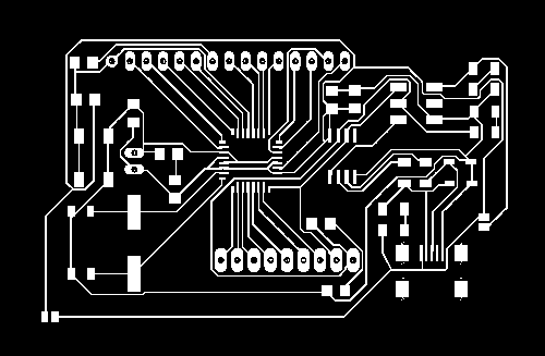

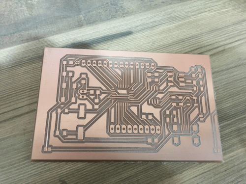
This was the final PCB which was printed.
After cross checking the board I started with placing components over the board
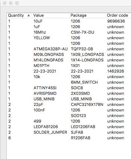
Here is the list of components which were neede to complete the board
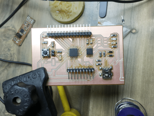
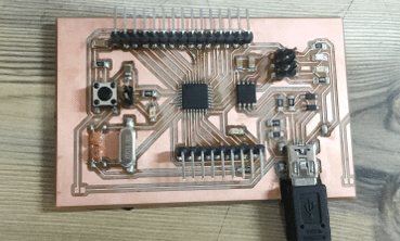
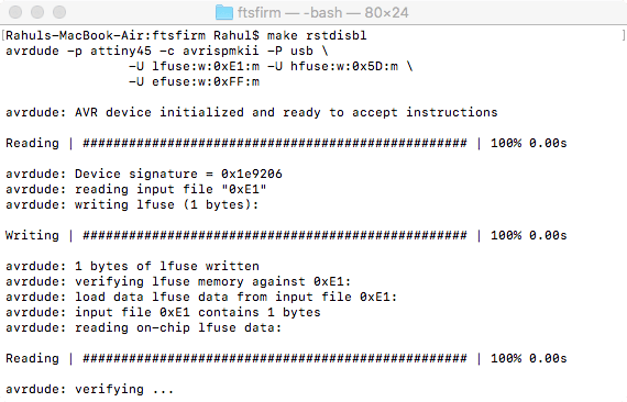
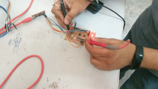
After Soldering all the components it was time to program ATTINY 45 on board
For programming ATTINY 45 I connected the MOSI MISO Pin with the ISP header externally, Check Video Below
For programming simple connect the ISP Header and using this FIRMWARE flash the Chip.
Everything went smooth and now the board is detected on USB
 Download Firmware
After this it was time to program the main 328P chip and test weather the board was working or not .......
The first step is to burn bootloader
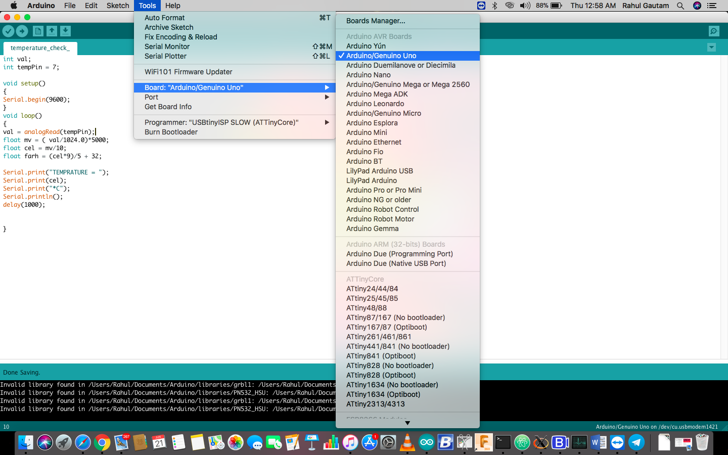
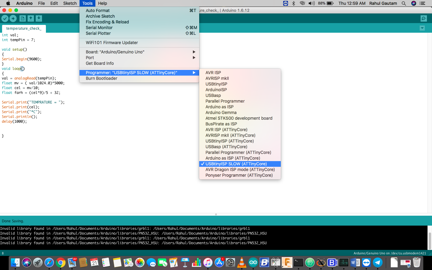
For burning boot loader ..... Firstly select Arduino UNO in Boards menu and then USB TINYISP in programmer menu .....
Now in tools Click Burn Boot Loader
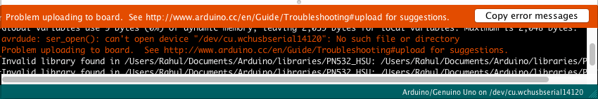
Bootloader was burned but with errors.
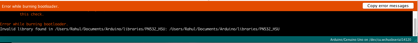
Now since the bootloader was uploaded even tough with some errors, I tried to program the board with basic Blink Program..... Which I was unable to do .....
Conclusion
To select individual controller on board we need to externaly connect the MOSI MISO and RESET Lines which were left unrouted while making PCB, ATTINY 45 has to be programmed only once.
I went through lot of online forums to check this error, mostly said .... The computer is unable to open Port ..... I was not able to find any solution .... but still I am working on it to find a proper solution....
My this weeks assigment was not completed as I was working on this board ..... So I decided to make a common board for both Input/Output and make it in next week ..... till then ...... DEBUGGING.......
This has been documented in next week week 12 i.e Output Devices (LINK)
Download All Files Download Board filesHere I am documenting about one of the input devices I used in my final project
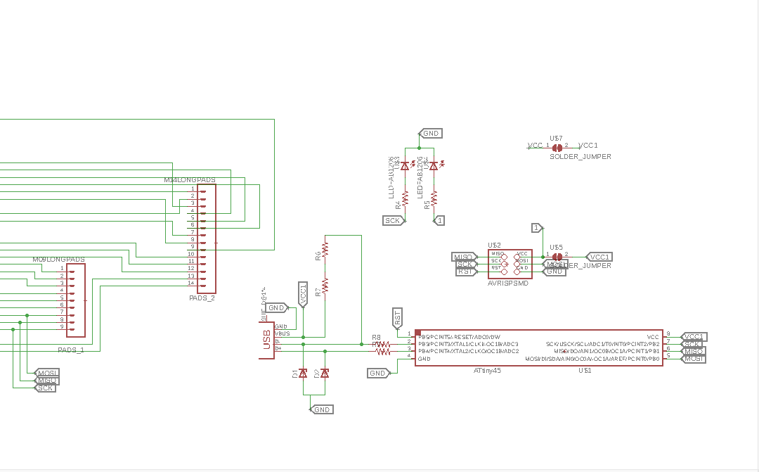
Sneak Peak at the Final Board
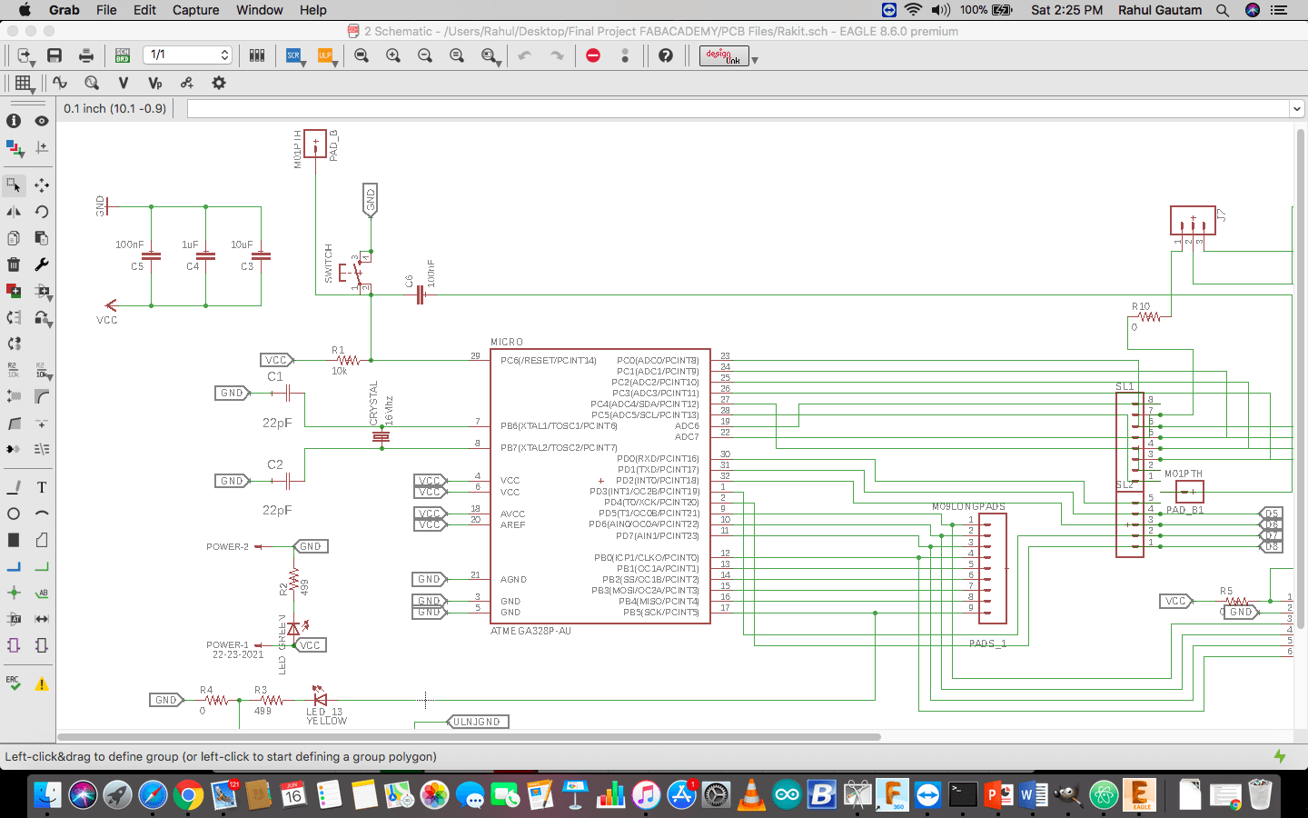
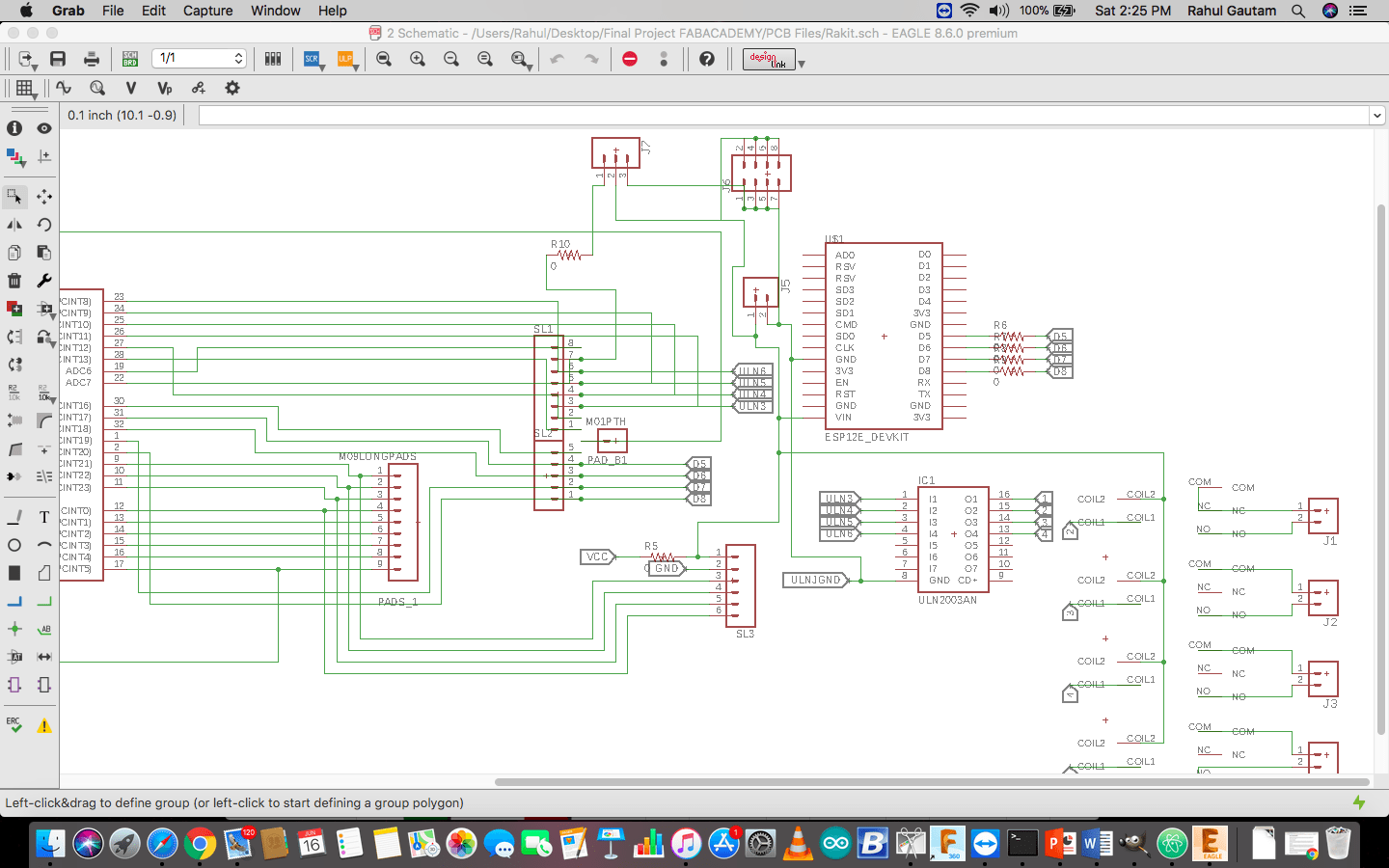
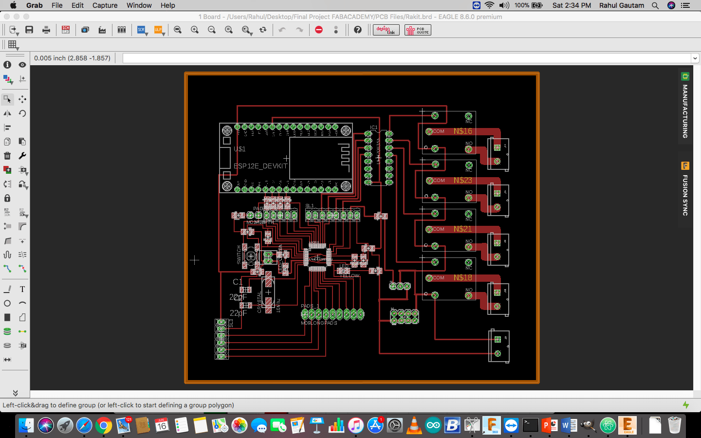
Now here is the Board layout
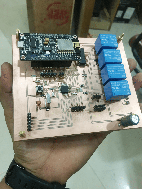
For detailed explaination refer this link Final Project Documentation
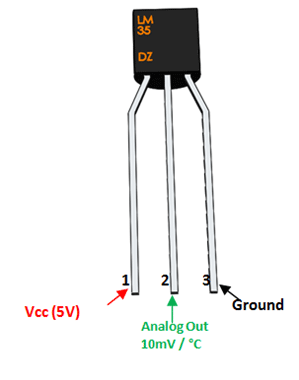
Temperature Sensor LM35
Description
The LM35 series are precision integrated-circuit temperature devices with an output voltage linearly-proportional to the Centigrade temperature. The LM35 device has an advantage over linear temperature sensors calibrated in Kelvin, as the user is not required to subtract a large constant voltage from the output to obtain convenient Centigrade scaling. The LM35 device does not require any external calibration or trimming to provide typical accuracies of ±¼°C at room temperature and ±¾°C over a full −55°C to 150°C temperature range. Lower cost is assured by trimming and calibration at the wafer level. The low-output impedance, linear output, and precise inherent calibration of the LM35 device makes interfacing to readout or control circuitry especially easy. The device is used with single power supplies, or with plus and minus supplies. As the LM35 device draws only 60 µA from the supply, it has very low self-heating of less than 0.1°C in still air. The LM35 device is rated to operate over a −55°C to 150°C temperature range, while the LM35C device is rated for a −40°C to 110°C range (−10° with improved accuracy). The LM35-series devices are available packaged in hermetic TO transistor packages, while the LM35C, LM35CA, and LM35D devices are available in the plastic TO-92 transistor package. The LM35D device is available in an 8-lead surface-mount small-outline package and a plastic TO-220 package.
Features
Calibrated Directly in Celsius (Centigrade)
Linear + 10-mV/°C Scale Factor
0.5°C Ensured Accuracy (at 25°C)
Rated for Full −55°C to 150°C Range
Suitable for Remote Applications
Low-Cost Due to Wafer-Level Trimming
Operates From 4 V to 30 V
Less Than 60-µA Current Drain
Low Self-Heating, 0.08°C in Still Air
Non-Linearity Only ±¼°C Typical
Low-Impedance Output, 0.1 Ω for 1-mA Load
   int val;
   int tempPin = 7; // Declaration of input pin A7.

   void setup()
   {
   Serial.begin(9600); // Serial communication started
   }
   void loop() // Endless loop
   {
   val = analogRead(tempPin); // Input taken from pin
   float mv = ( val/1024.0)*5000; // Input convrted to voltage
   float cel = mv/10; // voltage converted to temperature as LM 35 Output changes 10mV/1 Degree Celcius
   float farh = (cel*9)/5 + 32; // Temp. in Farenheith

   Serial.print("TEMPRATURE = ");
   Serial.print(cel); // Serial print Temp.
   Serial.print("*C");
   Serial.println();
   delay(1000);
    }
My final board is an upgraded version of Satshsa kit, but the pin configration is same as that of satasha kit.
> So here are the connections to Program the board
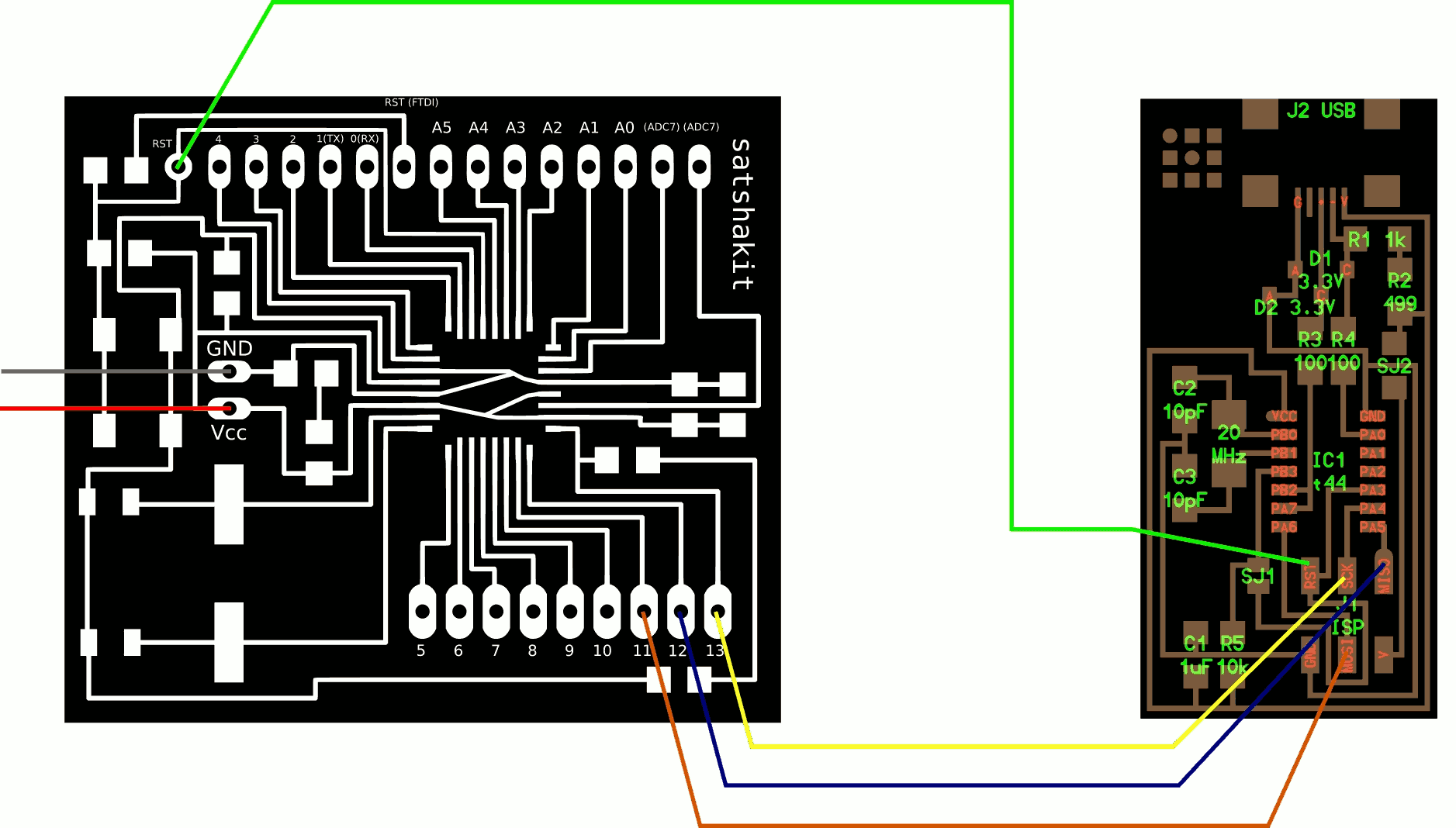
Img Ref: http://fabacademy.org/archives/2015/doc/projects/satshakit/satshakit.html
> The LM35 Output pin is connected to ADC 7 on the board (A7) in arduino IDE, This pin was choosed because, the other Pins were used to actuate the relays and only these pin were left, Also ADC& or A7 was analog input pin and the output from the sensor was also supposed to be analog ( 10mV per degree Cel ).
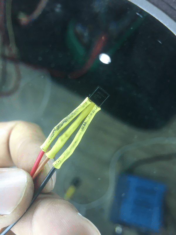
> The placement of Sensor is away from the main circuit board as the user might want to measure the temperature of a particular place rather than the circuit boards temperature.
> The Serial data is collected using FTDI Convertor. Whose connection are as :
FTDI Board      My Board
Vcc  --------> Vcc On Board
Gnd  --------> Gnd On Board
Rx   --------> Tx ( Pin 1 )
Tx   --------> Rx ( Pin 0 )
Settings while Programing
The Program would COMPILE, BURN and WORK Properly & Normally
In my Final Project I have used OLED as the output device and RTC & Temperature sensor as the input device, for more details visit Final Project Documentation
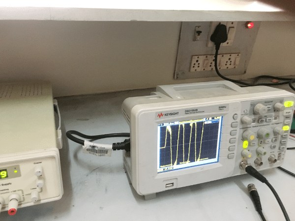
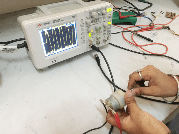
Group work - Input Devices
Measuring Digtal Input
Here Blink code was uploaded to the Board which we named as RAKIT, and the DSO probes were placed between output pin and ground
Code
void setup()
{
pinMode(13, OUTPUT); //  initialize digital pin 13 as an output.

}
// the loop function runs over and over again forever
void loop()
{
digitalWrite(13, HIGH);   // turn the LED on (HIGH is the voltage level)
delay(1000);                       // wait for a second
digitalWrite(13, LOW);    // turn the LED off by making the voltage LOW
delay(1000);                       // wait for a second
}
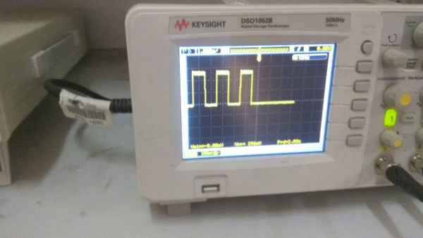
Observations
Measuring Analog Input