Week 5
Getting started with Electronics Production
This weeks assignment was to get a hands on with electronic circuits and make your own ISP Programmer, which is supposed to be cool....... To get started with electronics production I started with reading all the content over the fabacademy schedule....... I went through all the boards and tried to understand them ....... and decided I'll make atleast two type of programmers for myself........ To get started I started with characterization of our machine i.e SRM 20. I downloaded the PNG file from the Fabacademy Schedule page .... then Using Fabmodules I made .RML file and finally it was milled...... It was a group assignament...... After the final milling the results were not so good ..... we realized the tool was not sharp from the end and it needs to be replaced ......
Conclusion
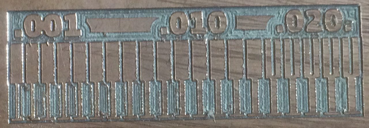
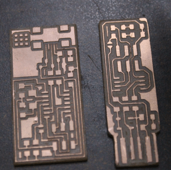
This test was performed to check the capability of the machine..... In this mill job test tracks from 1 Mils to 20 Mils were made.... and from the image it may be concluded that the machine was able to print 1 Mils also, but the track quality is not upto the mark, It was observed that the tracks above 12 Mils were perfect.
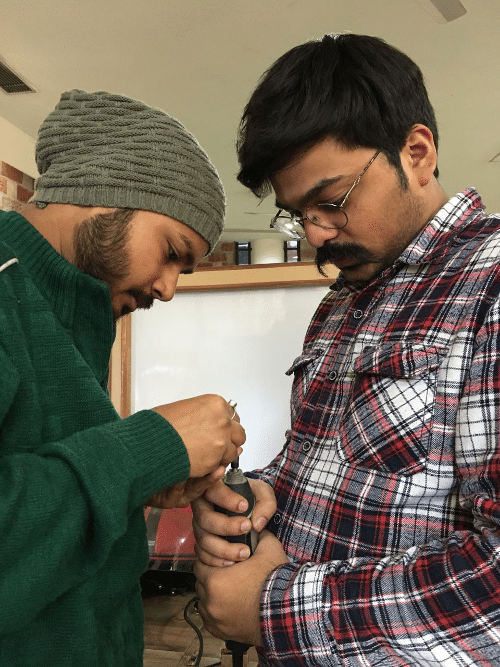
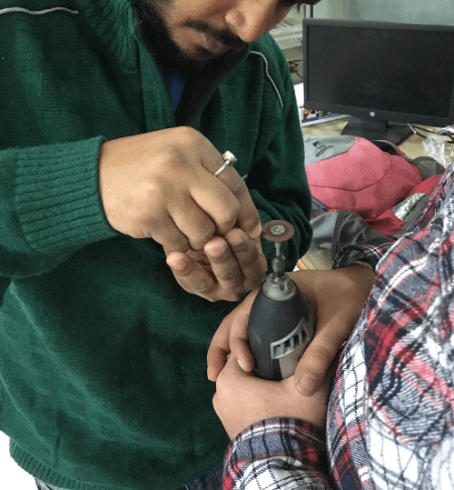
Replacement of tool at such an urgent basis was not possible so we decided to grind the tip of the tool using dremel..... The results were totally uncertain but some how we managed to make that tool usable ........
WARNING
Be very much careful while using grinding tool...... If possible do it under supervision .... and keep some water near you .... The bit may get really hot ......
Time to mill PCB & Solder
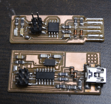
Soon after we have a working tool again ..... I started moving ahead to mill the pcb...... I have decide to make atleast two types of programmers.... I downloaded the files from the Fabacademy Schedule page.... The two Programmers I was going to make were :
1. The one with a crystal (Neils Board)
2. The one with a USB Stick ( Brians Board )
Source : Fabacademy/Archive/2018/Schedule
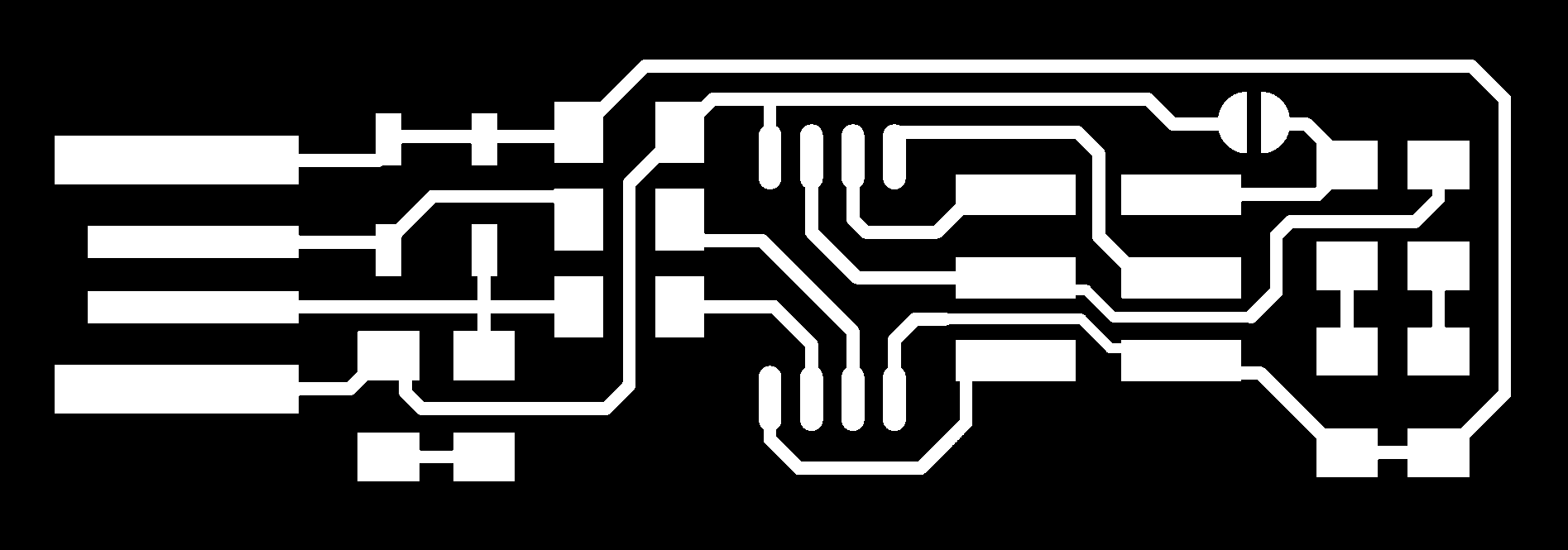
Afer downloading both the files along with their border's. I made RML using Fabmodules.org.
Making .RML File
For making .rml file I used Fabmodules.org
Here is the step by step guide to generate the .rml file
Step 1: Open Fabmodules.org and select the input format as Image(.png)
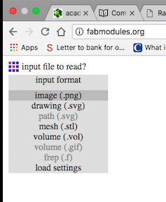
Step 2: Open the file (.png) and select the output as .rml
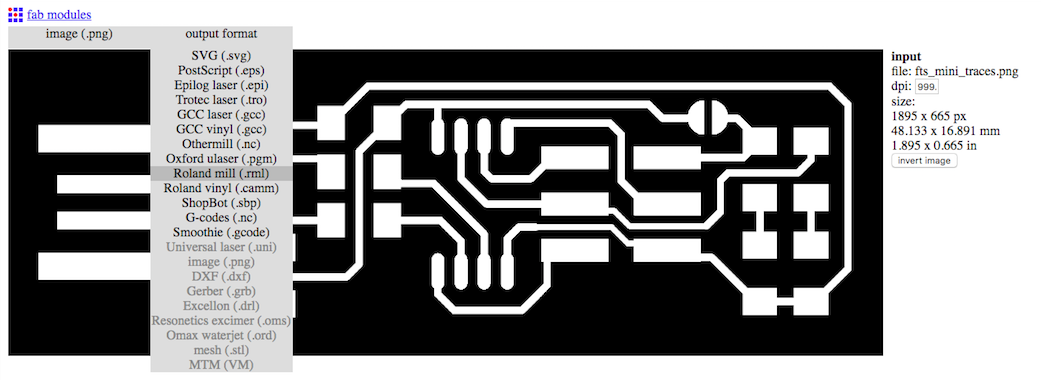
Step3: Now select the process as PCB Traces (1/64) as we are going to mill the traces for outline we'll use PCB Outline (1/32).
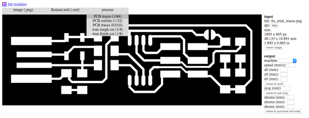
Step4: Now Select the machine which is in our case SRM 20
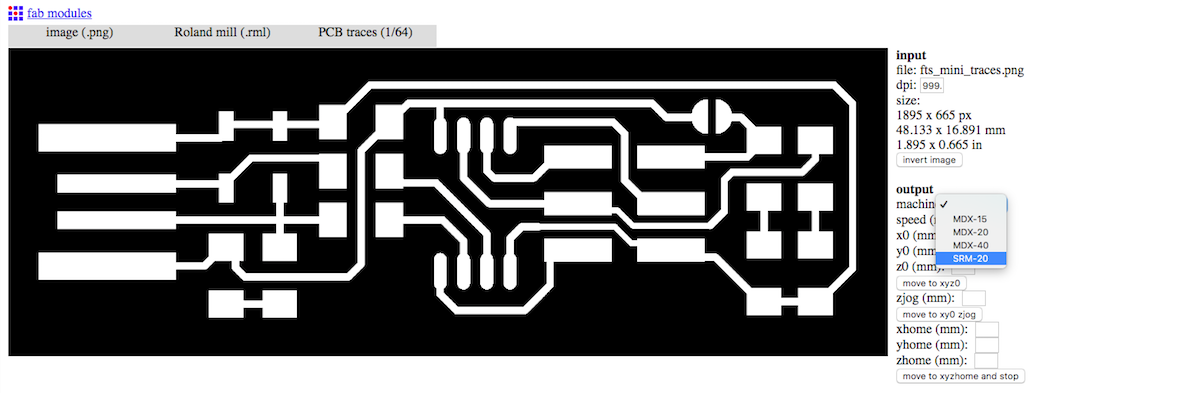
Step5: Now set the parameters as : and then click on save to download the file
Tool Diameter is the diameter of the tip of the tool, For tracing we use 1⁄64 and to cut the outer edge we use 1⁄32. Since in our lab we use a V-bit instead of the 1⁄64 bit, thorugh some trial and error TOOL DIAMETER of 0.4mm works best for us,
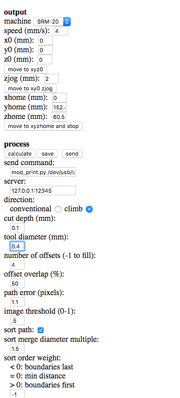
Step6: Now after downloading the RML file, it time to mill out the board. Open V panel for SRM 20
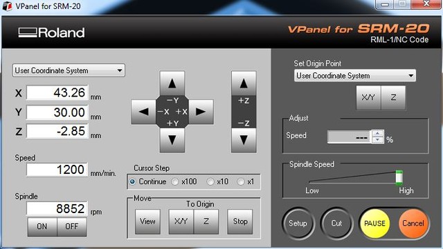
Step7: Now go to CUT button and select the downloaded RML File followed by clicking on Output
Precautions :
> Make sure that the CLAD Board is fixed properly over the Machine bed..... otherwise during milling it may unstuck and it would be printing something else ....
> Before giving a cutting command over the V panel make sure that the origin has been made according to the clad board and preevaluation of the space should be done before.
> If you are allergic to dust you should wear a mask, learned this ...... bad way ..... I am allergic
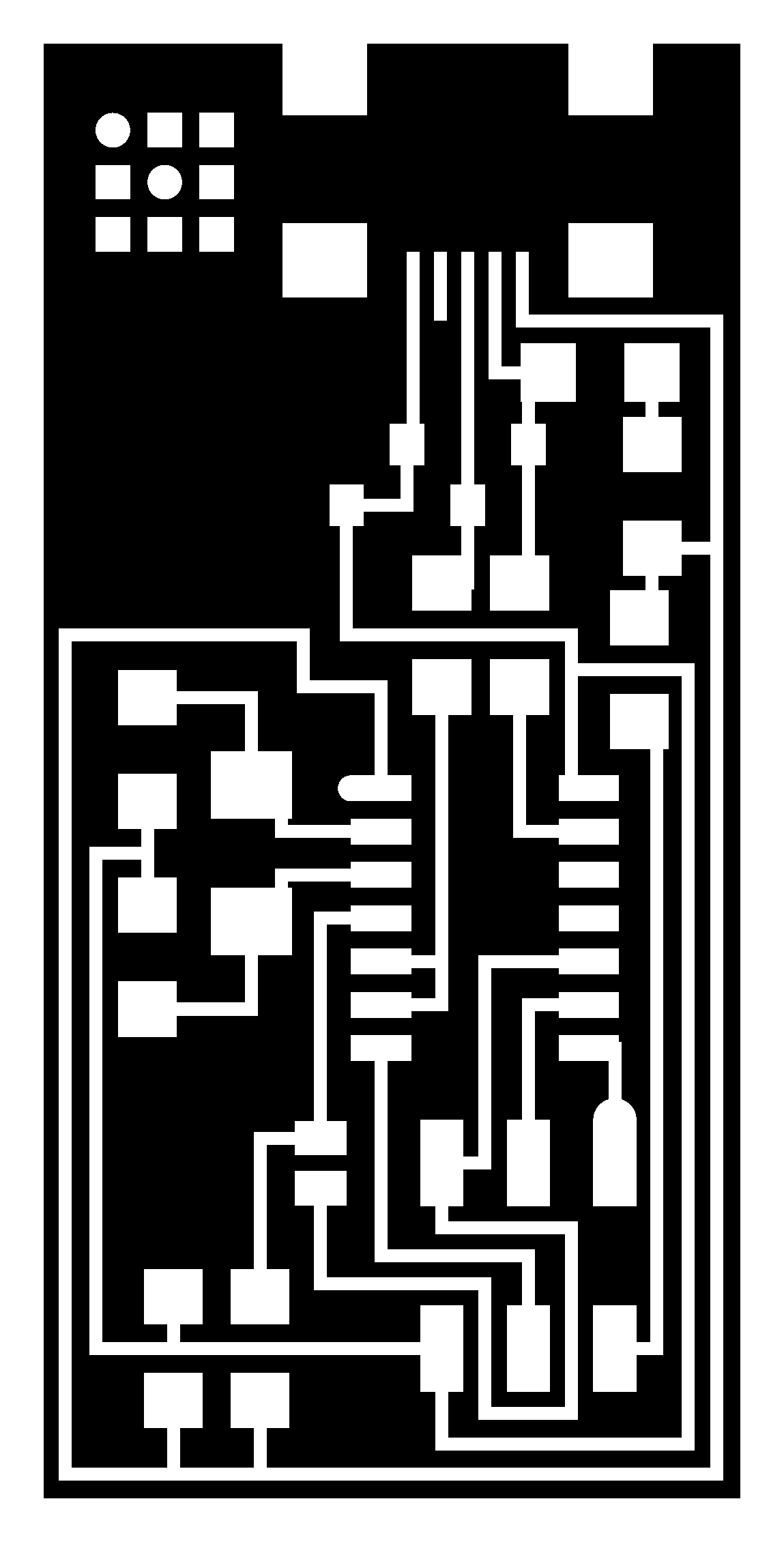
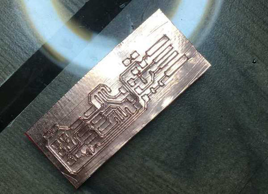
Now taking care of all the things, since our tool was custom modified so the statndard parameters which we gave were not enough to Mill out a proper PCB. So, We modified the parameters as : Cut depth was increased to 0.12mm which was earlier 0.1mm, apart from that tool diameter was also incresed from 0.35mm to 0.4mm. After setting the parameters the final milled PCB's were as :
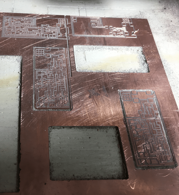
After millng the PCB I cleaned it with cloth and then a sanded it a bit with low grade sand paper so as to get a smooth and clean finish ........ After this step I listed down all the components and get them issued from the inventory ...... This step is dammmmm annoying ....... After this I started with soldering .....
Before Soldering, I did some ground work and arranged all the tools which could be required for doing the job .........
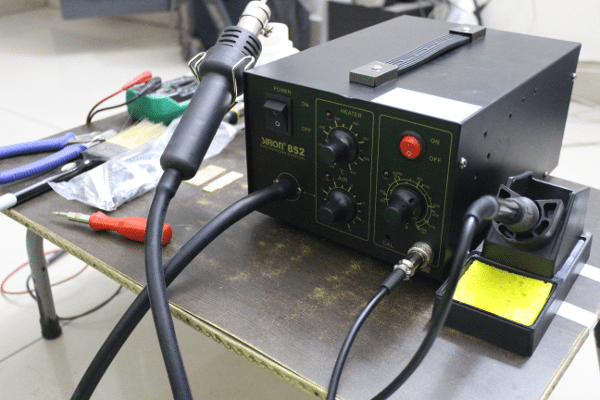
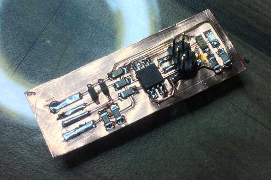
For soldering I used a combination of reflow method and fine tip soldering iron. For soldering IC and Crystal I used Reflow and for other components I used fine tip soldering bit.
Time to Program and get some extra Credits
After soldering all the components over the board its time to test ......... whether it works or just a beauty .......... So I started with learning the tutorials over the class page....... I intsalled crosspack AVR for MAC, GCC and Make were already installed....... so I just checked their versions ....... That was ok... I dont ned to update them........
I downloaded the firmware from class schedule page...... and followed the instructions as given on the programming section of the page.
The steps I followed to Program Hello ISP without Resonator one are :
> Download the firmware
> Extract the firmware
> Open Terminal
> Enter into the folder which has the firmware using CD Commands
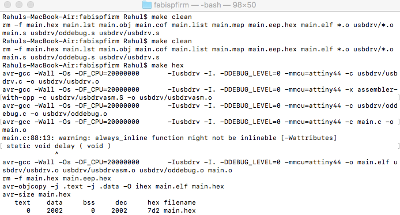
> Run Command $ Make Clean
# This command would be cleaning any files which were earlier created to configure the board
Open the make file with a plain text editor ( ATOM, SUBLIME, NOTEPAD ++ etc) and search for usbtiny (this is the programmer which we'll be using to program the board .... In my case it is AVR ISP MK2) and replace it with the program you have.... In my case I replaced it by AVRISPMKII.
> Run Command $ Make hex
# This would be creating a hex file of the firmware which would be uploaded to the board afterwards
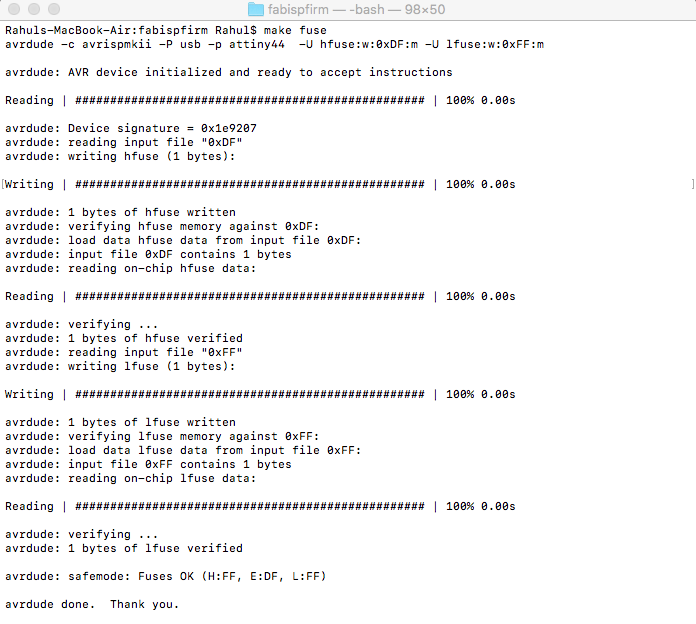
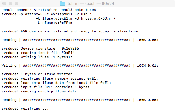
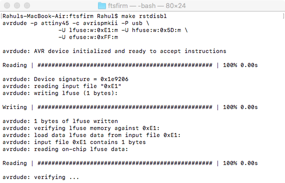
> Run Command $ Make Fuse
# This would be setting the fuses
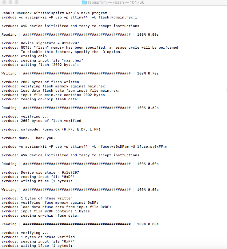
> Run Command $ Make Program
# This command would be burning the program onto the Board
If everything goes right, then you wont see any error over the terminal...... otherwise there maybe some problem .........
> Now remove the solder jumper SJ1
# This will make sure that the computer recognizes it as a programmer.
In My case.... In first attempt I failed....
Here's what I did....
Everything seemed to be normal, I followed all the steps precisely .... but from here the problem started....
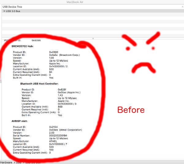
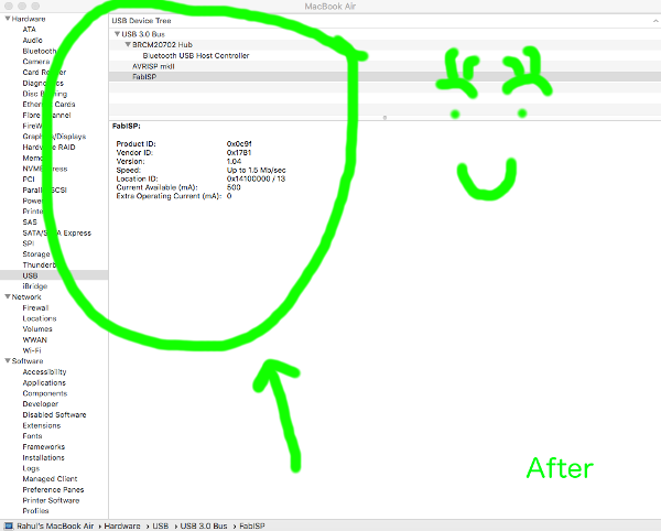
Everthing was OK .... Board was programmed properly ...... After that SJ1 was desoldered.... but the problem was after all this ... when I checked into my USB device tree there was no FABISP.......... I tried to program it again and again.... but the same problem was there ......
After a lot of efforts on the software end ...... I finally understood the problem is within the board .....
So I changed my mode to troubleshooting mode and evaluated each solder joint and resoldered any suspicious joint........
Well , this was also of not use ........ again same symptoms....
I decided to make a new PCB with all new Components .... but my Instructor asked me to spend some more time and troubleshoot what's the problem.....
While troubleshooting I removed the crystal oscillator and tried to program it without oscillator........ I know ... thats a lame thing to do..... But this step only sparked me a solution.....
While programming it without external crystal it showed some errors, denoting yes it is talking .......... and properly trying to find external clock..... then I replaced the crystal with a new one ..... wooohhhhhhhoooooooooooo ! success ..... This small moment was happiness ...... It worked like a charm .... Now I was able to detect the programmer
Crystals oscillators dont fail normally ...... Probable reason for its failure ..... I used reflow method to solder it ....... may be I over heated it ....
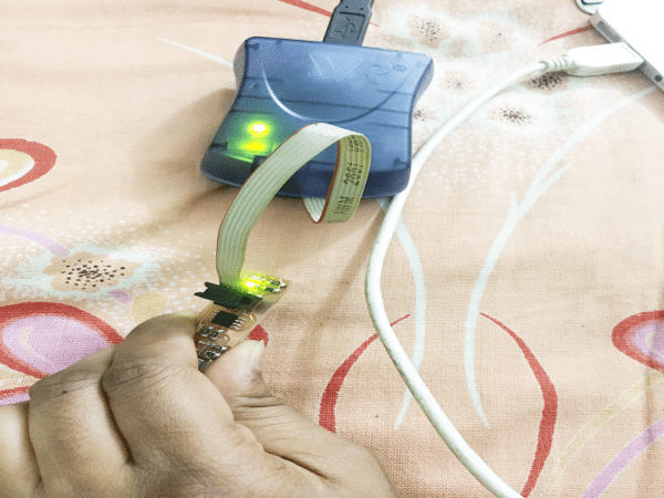
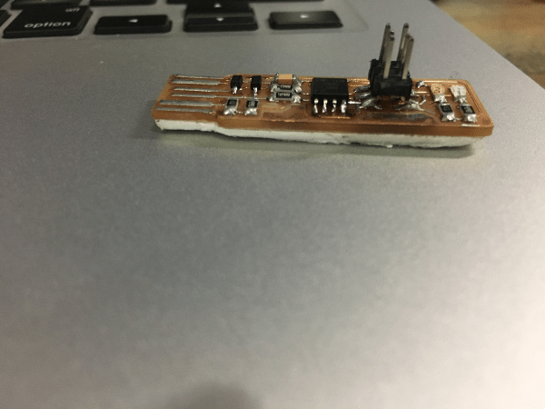
Now its time to program FTS_FABISP
I followed the instructions from Brian's page...... I followed each and every instruction properly but again First time, I failed to do that . I tried again and again ......... Firstly I thought it may be due to loose fitting of the USB..... I tried to plug it into so other PC but again same problem was there.......
This was the Error I was recieving when I was trying to flash it
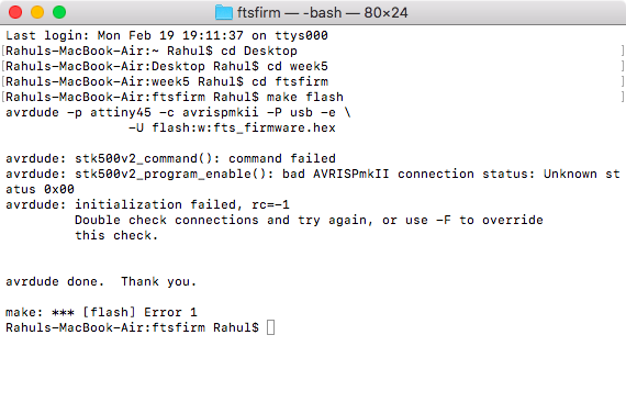
Troubleshooting
After several tries on this ....... I was convinced that the problem is from the hardware side .......
Firstly, I tried to match the board with other students board from previous years ..... and then I found one disparity in my board ..... The zener I was using as not 3v3 .... So I changed it and again tried to program it ....... again same problem was there.......
From my previous experience ...... I thought may be this board is also having the same problem as the crystal of previous board was having ....... I used the same process of reflow to solder ATTINY 45 on this board....... I replaced it ..... and then tried to program it ...... again same problem was there
Now I decided to have a closer look over the board and cheak every connection with multimeter ....... I found a small discontinuity in the path ...... and corrected it with a single stand of wire....... again I tried to program it ........ This time I was successfull to program it .....
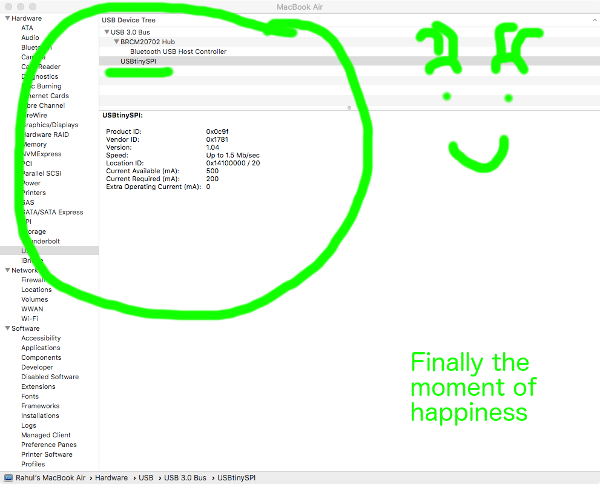
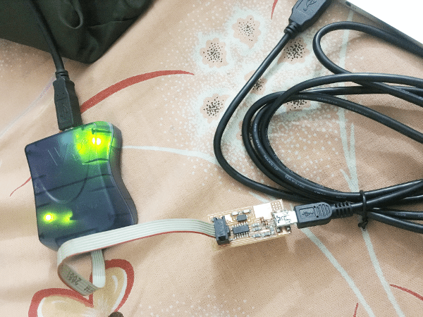
Now since my ISP programmer was discoverable on USB tree..... I can disable the reset pin ......
And now it's done ...... woooohooooooooo !
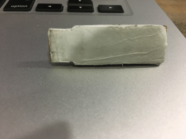
Now I faced one more problem ....... the usb stick was very loose ...... I have to set it again and again ...... but it was loose ..... I decided to make some padding so as to make a tight fit ..... I made a padding using a double sided tape and then I pasted a masking tape over it ....... and then with a fine knife I smoothened the edges, Now it was a perfect fit for the USB port.
How not to make Flexible FabIsp
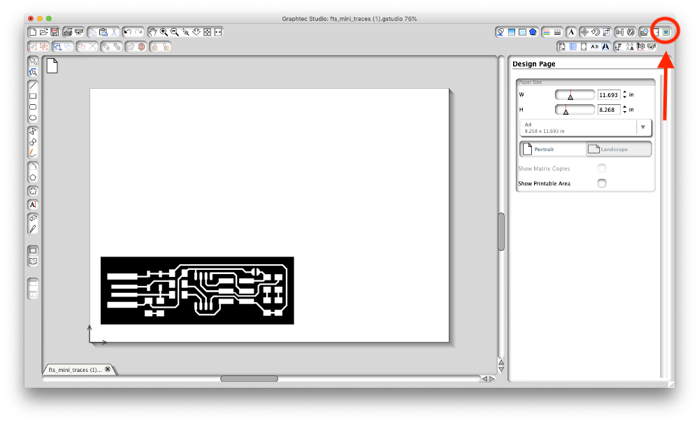
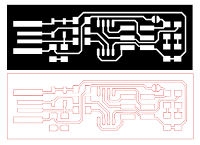
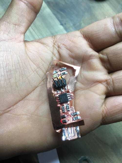
After my FabISP was working I decided to give a handson to Flexible circuit. For making a flexible circuit I order 3M copper tape, which is easily available on Amazon. I started with tracing the tracks of the programmer using Graphtec Studio.
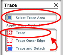
Now open the file in Graphtec Studio & click on Select Trace, marked red in Screen Shot
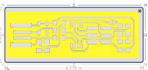
Now selecting the area I want to cut.
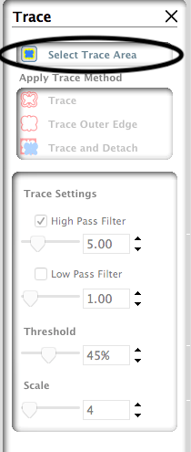
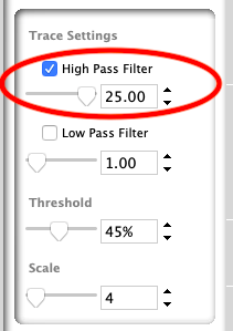
I noticed that some of trace area which I choosed was black, this is the area which cutter wont cut. I just wanted the traces and boundry, So I changed the threshold to maximum.
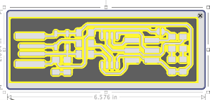
After the marked trace area was ok, I traced the tracks.
Now I moved the original file and deleted it, Which left me with just the traces.
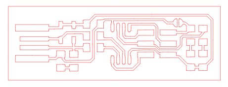
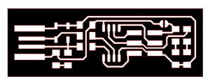
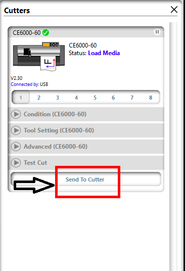
Now after this I sent the file to cutter & this was the output
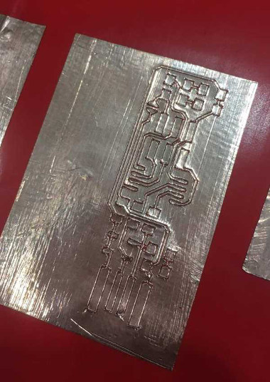
Now after the traces were cut I was a bit worried about its weeding as some of the tracks were too thin to be peeled off. So I decided to solder it first and then try weeding.
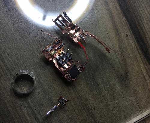
Initially I was a bit worried about soldering, but it went quiet well, Now I was supposed to weed it off...... #Worstpart (It requires a lot of patience, steady hands etc etc good stuff), I started weeding using fine pointed forcep, it went well until this happened.
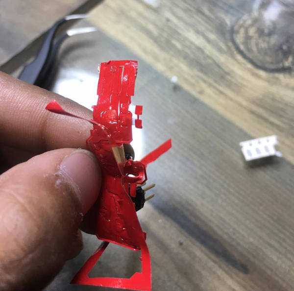
And........... it took its last breath ..... this is how you dont make a flexible PCB ....
Learning
The process which I followed is not an ideal process, it needs a lot of improvements...... Next time I'll try to do weeding before soldering....