Week 7
Getting started with Electronic Design
This weeks assignment was to recreate hello echo board with any of the PCB designing software along with addition of a button and a LED. For this week I used Eagle for designing the PCB. Points which should be considered while designing PCB are :
1. Task to be performed by the board
2. Design Consideration
3. Availability of components and raw material
4. Complexity of design
Also use the test equipment in your lab to observe the operation of a microcontroller circuit board
Getting Started
The first step I followed was to go ahead and make a schematic of the PCB on paper which I was trying to make.
I am from electronics background so, I considered some basic design rules to make this schematic on paper.... this may modify while working with the actual Schematic on Eagle ( Like I may add some pull down / pull up resistors ).
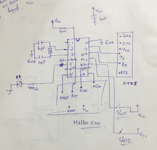
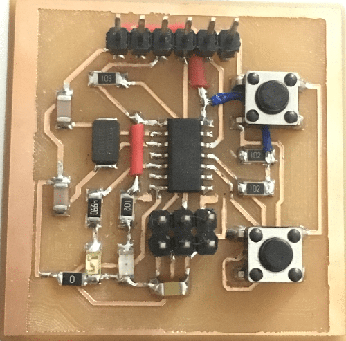
I decided to make a PCB which would be having 2 push buttons and a blinking LED along with the Power status LED. The 2 buttons would be serving the purpose of changing the time period of the blinking LED.
Getting started with Eagle
So basically Eagle is a PCB Designing software which can be downloaded from Autodesk's Website It also gives a student licence free of cost for 3 years, Students can redeem it very easily, its quite friendly to use and has a lot of capabilities.... So without much adu lets get started
You can follow this Video Link, For understanding eagle from scratch. I was a bit familier with eagle so I straight away went ahead with making schematics and PCB Layouts.
The first step is to make schematic and identify the package of the components which are to be used over the PCB. To make this easier I download Fab.lbr (Fab library). To add a library simply download Fab.lbr and add this folder to eagle library directory.
These are the steps which are to be followed to add a Library in Eagle
Step 1 : Download the Eagle Library ( which we have already downloaded ) Fab.lbr (Fab library)
Step 2 : Go to Library Button on the tool bar > Then Go to Library Manager
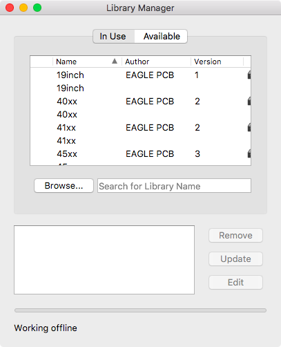
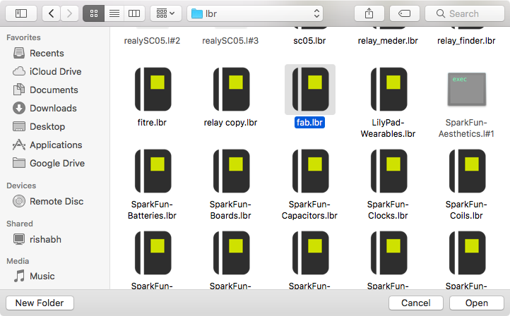
Step 3: Now in this window Browse the location where you have saved / downloaded the Library and then select the Library > Open button
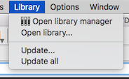
Step 4: Now go to library and then click on Update all
Step 5: Now we need to check wether the Library has been added or not, for that go to add components and check for the fab library
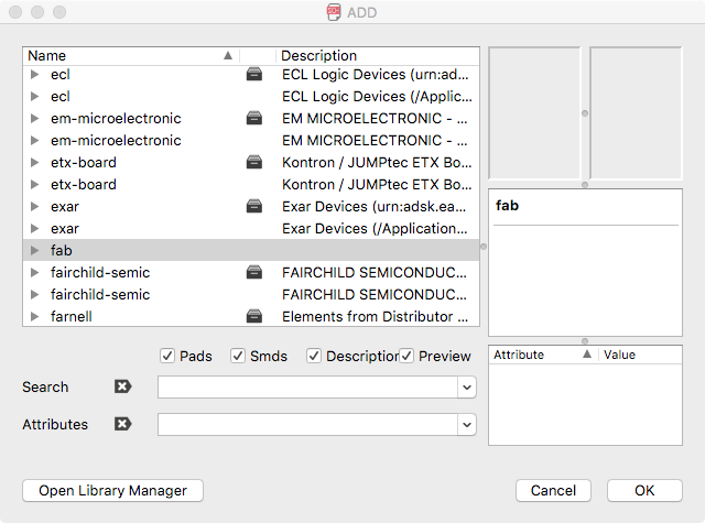
As you can see the fab Library is now visible in the component adding option.
Now in the schematic panel add all the components which are supposed to be used in the design.
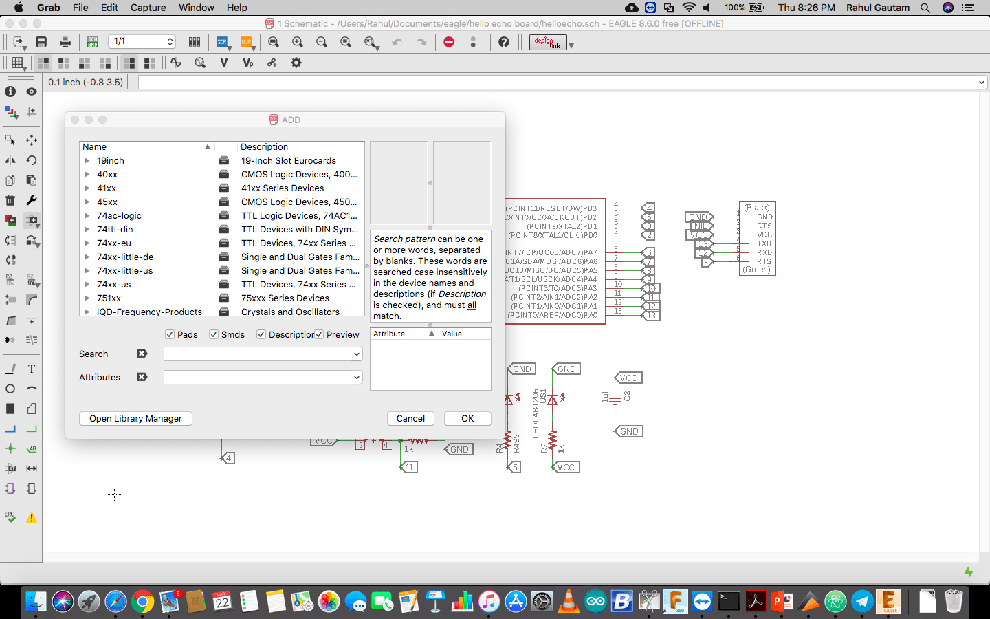
There are 2 methods to make a schematic either you can use path wires to connect all the components together. ( Its a bit messy method to make a schematic as it involves alots of crossovers and its very difficult to debug afterwards )
In the second method one can use labels to identify the connecting the point of contacts. ( This method is very much recommended as it drastically improves the visibility and clearity of the schematic and its very easy to debug and change afterwards )
Schematic
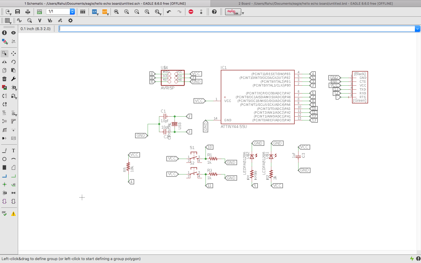
These were the steps which were followed to create this schematic
Step 1: After adding the Fab Library, Add all the components which would be required to make the schemtic.
Step 2: I linked all the components using Labels.

This AB Icon is the label tool
All the nodes with same labels would be connected to each other
An exaple of label is as shown below
In this picture VCC and 4 are the labels
Now that my schematic is ready its time to make the Layout file.
Board Layout
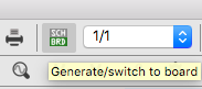
Now to convert this schematic to Board layout we need to click on this Icon over the tool bar SCH BRD
Now move ahead with this Window
\
Now a new window would appear which would be like this
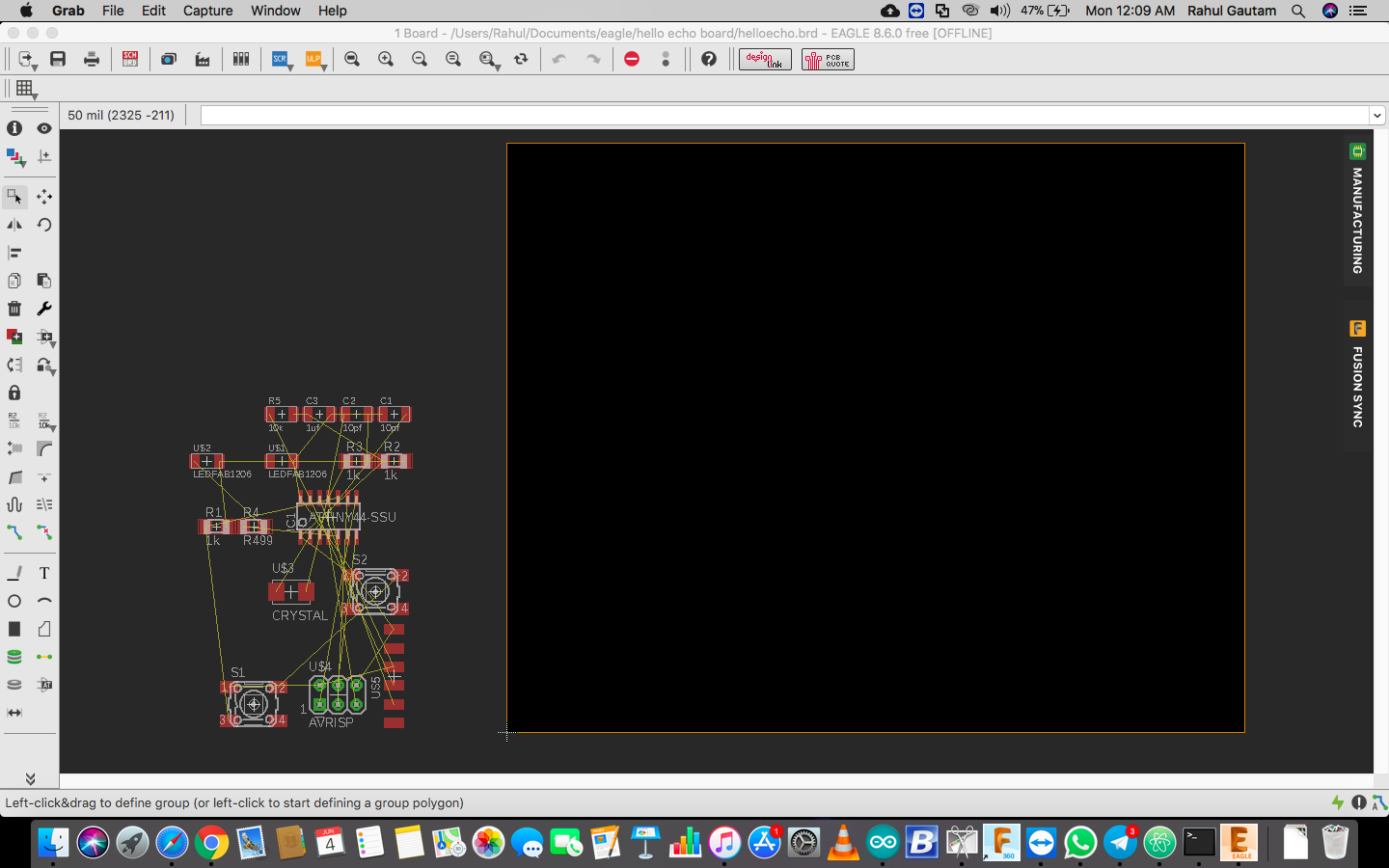
Now in this window the dark Black area within the orange boundary is our main work area or we may say this is the area which is going to be printed .... we need to put all the components within this area. This operation can be done using simple drag and drop.
Now I started to set the design rules and net list to make sure everything is within the limits of SRM 20.
Go to Edit and then Design Rules
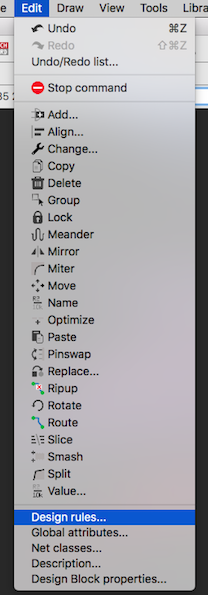
Opening Design Rules
Clearance
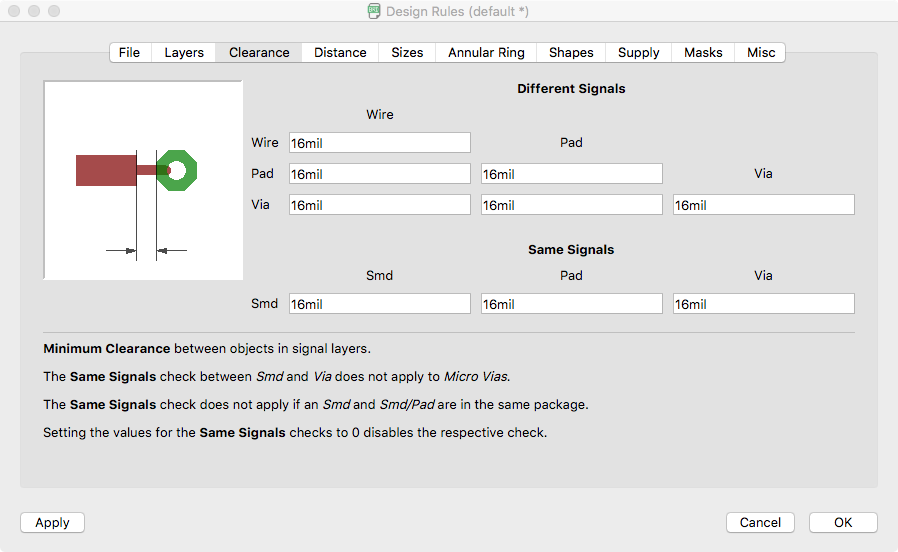
Now 1st thing we need to set is the clearance, In this window we would be defining all the clearances, either its betweeen two tracks or between tracks and pads etc etc ....., In our lab we would be using 1/64 bit so the trace would be about 16mils.
Distance
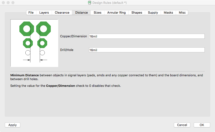
Corresponding to 16mils track I changed its default value by 16mils
Size
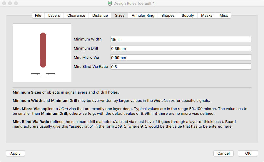
To be on the safe side I increased the size of the track to 18mils as 16mils was the minimum track width that my tool could have milled.
After setting all the design parameters, we need to run a ERC- Electronic Rule Checker

Click on the ERC Icon on buttom right side of the tool bar
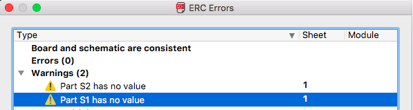
The rule checker shows some warning which are due to me, not giving values to some components ..... we can approve them all.... and now we are ready to start Routing.
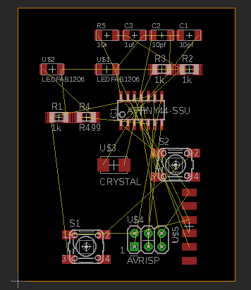
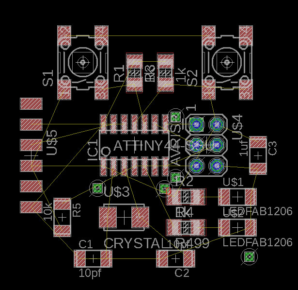
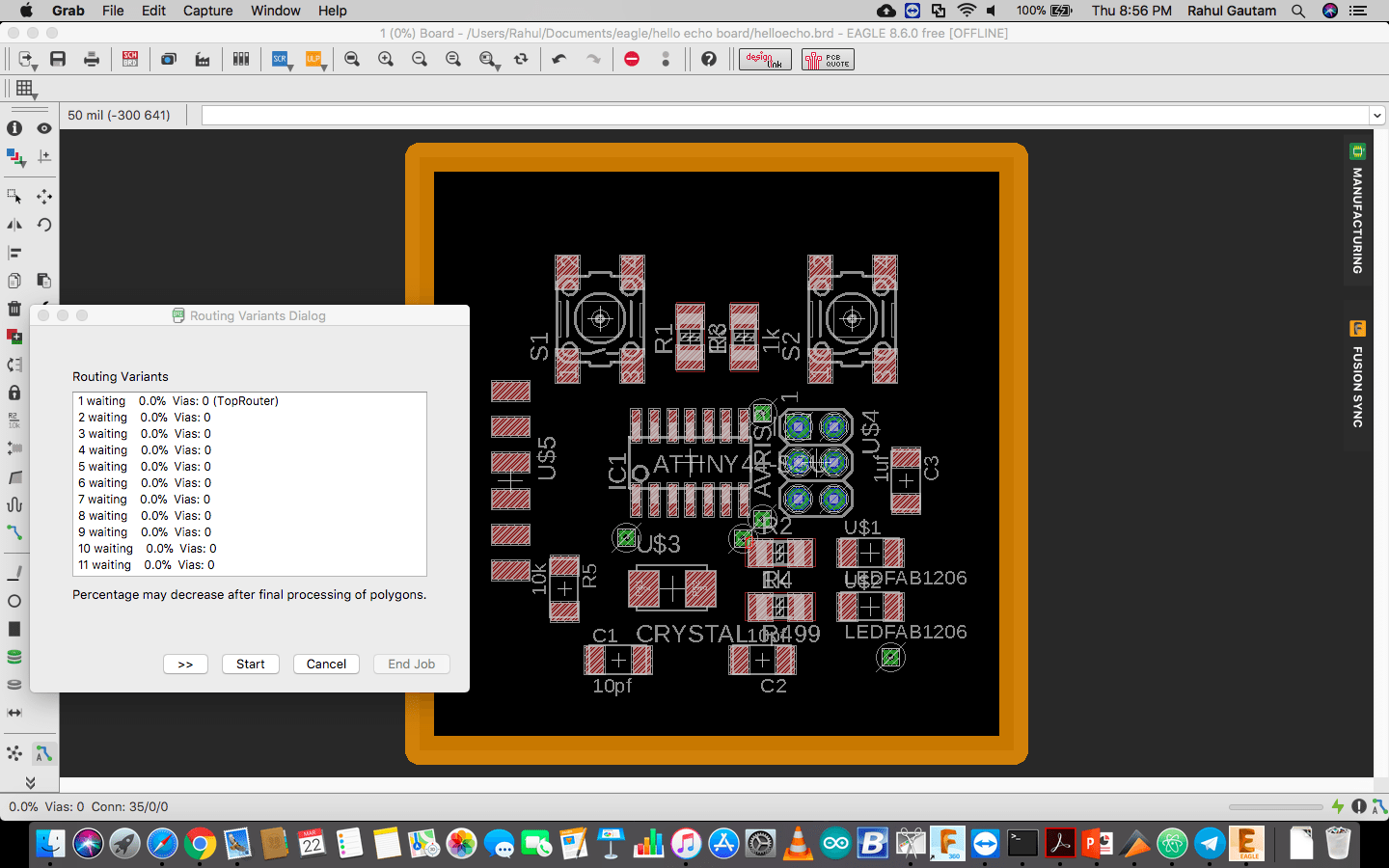
After setting all the rules we can move ahead with routing......it may be noticed that there are a lot of airwires which seems to make the board look complicated..... I used ratnest to clear out extra air wires and then I moved ahead for auto routing.....
Ratnest would clear out some nearest airwires
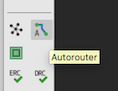
Now I used Auto router to route the PCB Tracks
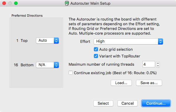
Make sure to choose bottom layer as "NA" to make a single layer PCB
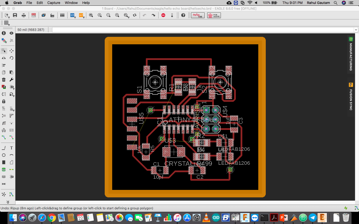
After Auto routing it may be noticed that few air wires are left, so after a lot of trials, I decided to leave them as it is and add external jumpers to complete the tracks
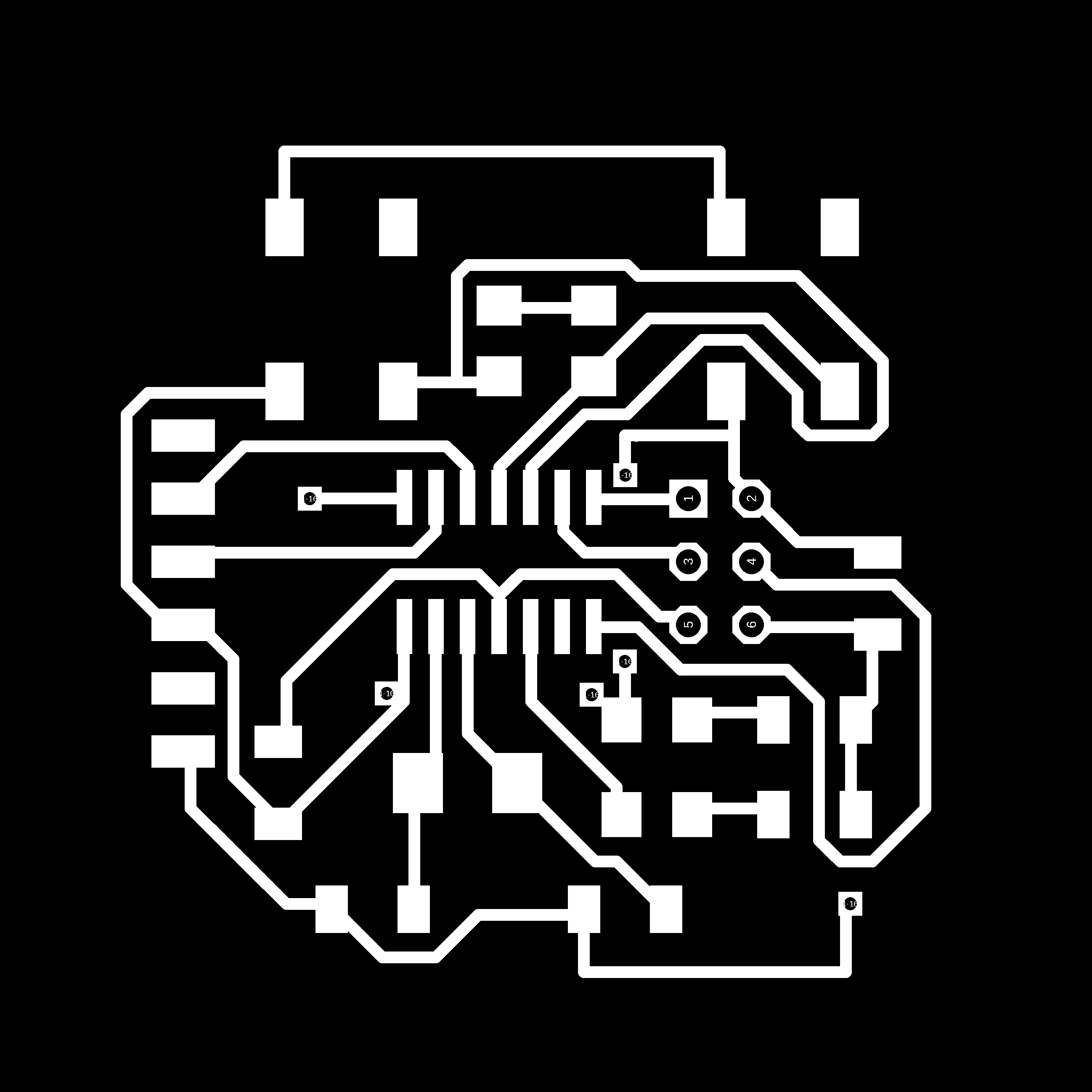
Exporting PCB File to Image
Goto Layers Setting

Click on this Icon to open the Layer settings Dialog box
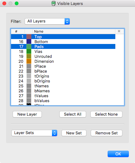
Now select the top and the pads layer and click on Apply
Note: This step is only for exporting the traces, Similar Steps have to be followed for tracing the outline of the PCB.
Now to export file to Image... Go to Files >> Export >> Images
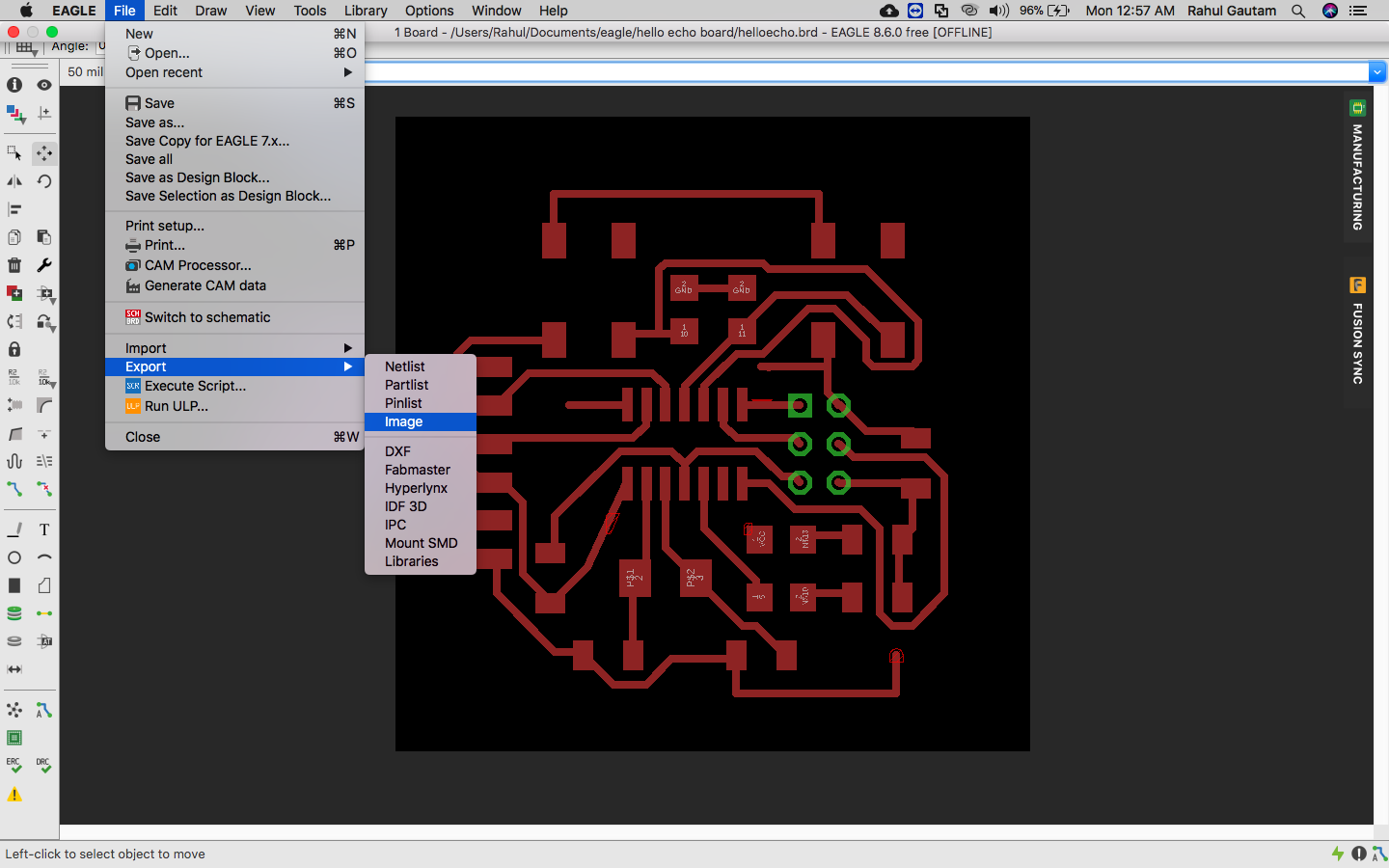
After this step a new dialog box would appear
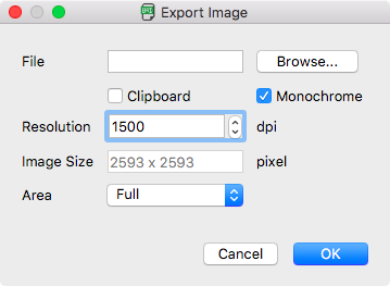
From this window you can select the location where to save the file...... and make sure monochrome is checked...... and also more the resolution better would be the quality.....

PCB Printing
Now we need to convert the .PNG files of the traces to tool paths ( .rml file ), I used Fabmodules to make rml files... the process is explained in electronic production week...
After final printing and soldering
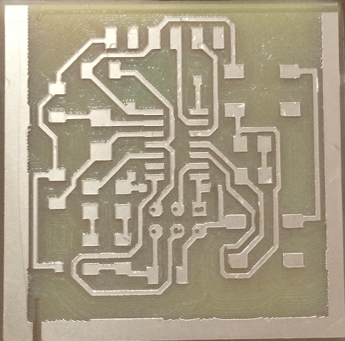
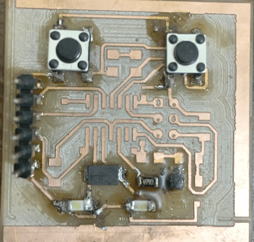
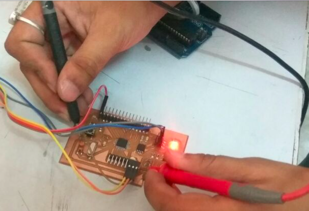
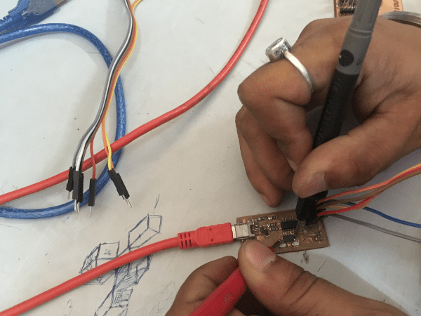
Now I went ahead to solder the components, here is a warning I used a overheated soldering iron due to which the tracks got unstuck and I have to print the PCB again.
Note: It may be noted that even after DRC I have left some Air wires, It is because of the complexity of the board, I fixed it using Manual jumpers, Also R1 & R3 should be at least 10K, otherwise, everytime you press a switch you will draw 5V/1k = 5mA current, But USB can give 500mA current, So that wont be an issue, but if someone out there is looking for some power efficient applications, You should use Pull Up Resistors rather than pull Downs like I hav done
Download all Files Download .brd/.sch fileLab Test Equipments ( Group Project )
Multimeter
A Multimeter is basically a Paramter measuring tool, which can measure a wide range of parameters, Principally : Voltage (AC/DC), Resistance, Capacitance, Conductivity etc.
Its the most common diagnostic tool technicians have, through multimeter debugging comes handy.
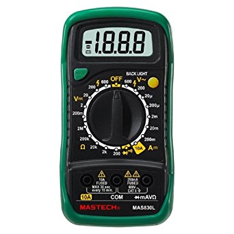
I used Multimeter to check the continuity of the tracks and make sure everything is connected according to the Board Layout
Power Supply
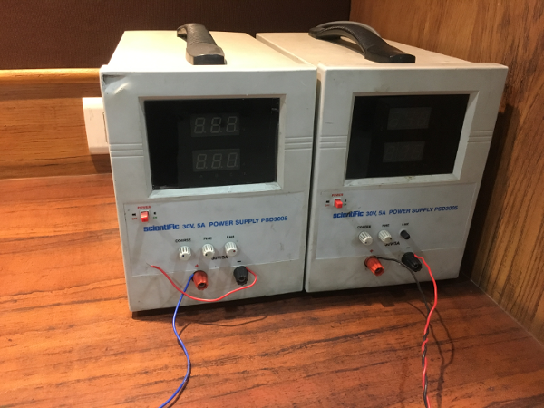
In our lab we have Scientific PSD3005 0-30V 5 Amps Power supply.
Features :
DC 0 to 30V, 5A
Constant voltage & constant current operation
Digital displays for voltage ¤t
Adjustable current limiter
Protection against overload & short circuit
I used this power supply to power up my board via Vcc=5v and GND.
Digital Oscilloscope
While working with electronics, for debugging and testing behavior, we need to understand the circuits on signal level, which multimeters fails to do...... In this case Oscilloscopes come in picture. A digital oscilloscope measures the signal, and then converts that measurement into a digital format using an ADC converter, after which the data measured is depicted as a digital waveform representation. From this representation various paramters can be evaluated.
In our lab we have Keysight DSO1052B which has the following capablities.
> Bandwidth = 50 MHz
> Channels = 2
> Max Memory Depth = 16 kpts
> Max Sample Rate = 1 GSa/s
> Display Size = 5.7 inch
> ADC Bits = 8 bits
> USB storage, RS232C and J45 interface
> Multi-waveforms math, FFT Function
> Built-in delay sweep function
> Waveform Record and Recall, Trigger Mode for Edge, Video, Pulse Width, Slope and Alternate
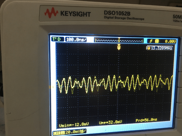
I tested the clock frequecy of my board
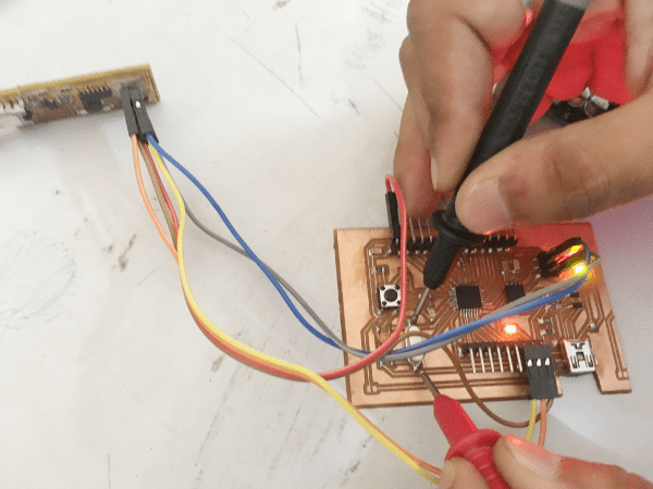
Also I tested the same for FABISP
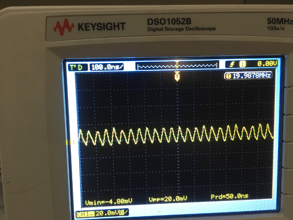
Observation
The Oscillator which was soldered on the board was 16Mhz, But the DSO was measuring 13-14Mhz (In case of RaKit), I dont know why it was happening, May be because of temperature or voltage.
The Oscillator which was soldered on FABISP was 20Mhz, and the observed reading was about 19.98Mhz, that seems perfect.