project development - Part 2
Continued from project development part 1
Step 4:
Create the board in Eagle
I made the schematic and board in eagle. I’ve documented the process in this document
Making the schematic + board in Eagle.pdf
I also used this tutorial from the IEEE department in our University.
Eagle Workbook.pdf
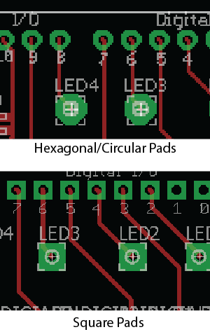
There are some extra changes I needed to make before I can engrave the board.
Firstly, the Denford PCB Engraver Software has trouble engraving the hexagonal circles so
I need to change these to square pads.
There shouldn't be any right angles along the traces so I used the Miter tool in Eagle to
alter the traces so they aren't at right angles. I also worked with the design rules to make
sure there was enough clearance between traces and pad. This is really important because
there needs to be enough clearance for the tool to get between everything. otherwise you might
end up with circuits accidently connected.
Finally some of the traces coming from the pads are too close to the pads so the tool won't be
able to get in between the traces.
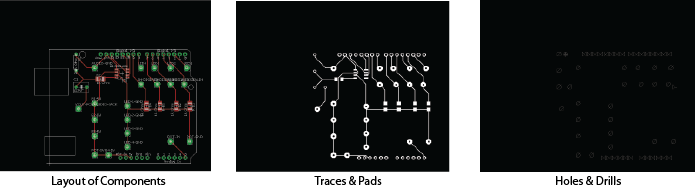
For Fab module or some other software you can use a png of the board but the
Denford software expects gerber files. You make these in Eagle software. I downloaded
Sparkfun Cam Processor Eagle Library
to do this. This website explains how to make the gerber files using the CAM Processor libraries.
Download files:
- Download the schematic
- Download the board
- Download the board gerber file
- Download the Drill file for the Denford-PCB-Engraver Software
- Download the FNC file for the engraver
Step 5:
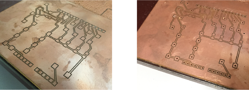
Milling the board on the Denford
To carry out the milling I follow a tutorial Iain for our Lab created for engraving
PCBs. Here's a link to the tutorial Iain made.
Once I imported the files to the Denford PCB Engraver software
Used 0.4mm end mill for engraving and a 1mm end mill for the drill holes. I changed these
over during engraving but the software will stop and ask you to change the tool in the middle of it.
Final board made from PCB-Engraver
Step 6:
Populating the board
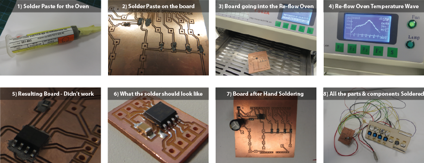
I had very few components to put on the board but I decided
I'd try the re-flow oven as I hadn't used it before. Unfortunately, it didn't work out for me.
I think I used too much paste. You can see in image 5 the solder didn't really flow as it should.
Image 6 shows how it should have turned out. In the end I decided to solder the components on by hand
as I only had 6 components going onto the board. I have a lot of external component off the board such
as buttons, pots and the audio jack. The end result of all the parts and components soldered together is
shown in image 8 below.
Step 7:
Programming the board
I created the code in arduino IDE and upload this to the arudino board. Then placed the shield with the DAC on it
onto the arduino board.
I had already created code and tested it on a breadboard before fabricating the PCB. So the next thing to
so was alter this slightly to work with the fabricated board.
This meant mapping the pot reading to match a frequency that would actually move the cornflour.
Download the final code I used here.
Step 8:
Testing the board with the Speaker
I was using a pretty old oscilloscope so I needed to use the formula for frequency
(wave period = 1/frequency) to worked out the frequencies of the waves I was generating.
The cornflour moved with the following frequencies and waves:
- Sine wave 6.7Hz - 87Hz
- Triangle Wave 13Hz - 108Hz
- Saw Tooth Wave 15Hz - 106Hz
- Square Wave 6.7Hz - 40Hz
Here's a video of testing.

Continued on project development part 3