W_06: Electronics design (Mar 4)
For this week we had to design our own circuit board, and what I did was use a program called eagle where you are able to create a schematic for your board and later on translate it to the board layout of your board.
EAGLE
What I did first was watch a couple of tutorials, that our instructor Ferdi sent us by email, on how to use the interface of eagle because i had never made shchematics or board layouts:
· Tutorial 1 for Eagle: Schematic Design
· Tutorial 2 for Eagle: Printed Circuit Board Layout
DESIGNING THE SCHEMATICS
To be able to design our board it is necesary to build a shchematic of the board and later on distribute the components on your board layout. Once you know this its time to start the schematics.
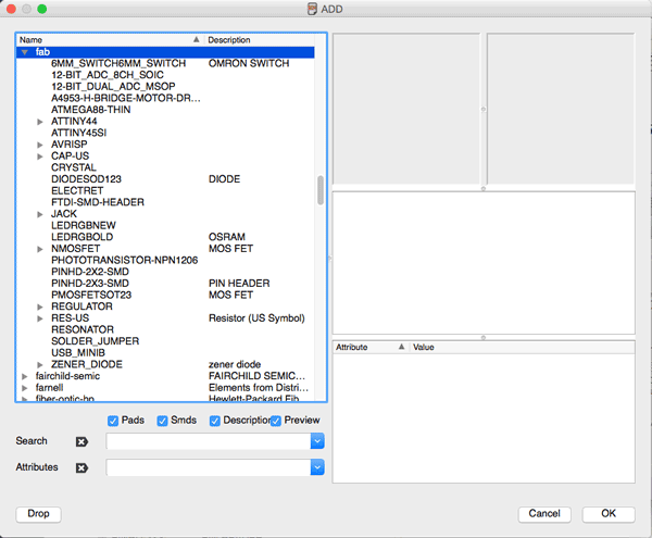
First of all you need to download a version of eagle compatible with your computer. After this you must have a list of all the componenyts that you are going to use to make your board(ours was provided by our instructor at fablab barcelona. Once you have this you need to save the components list in the eagle library, it should appear like this:
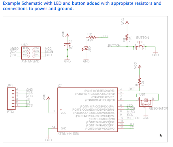
Now that I have this in place I started to find all the correct components and placing them in the schematic work area. I followed the schematic design provided by the tutorial on the POVIDENCE TUTORIAL WEBSITE.
Wich I made almost the same just because I'm very new in this area of work and didn't want to make any mistakes. This is the schematics i followed:
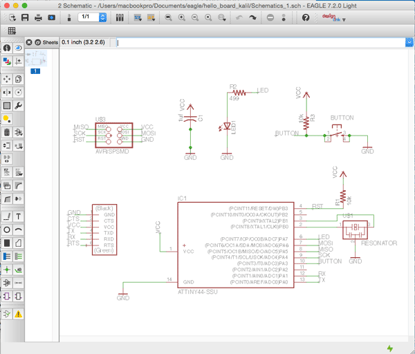
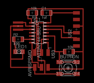
Here is a screen shot of my schematics after positioning all the components and names accordingly:
MAKING THE BOARD LAYOUT
After finishing the schematics it's time to compose the board layout. To do this there is an option in eagle where you transform the schematics to the layout mode. I followed a visual reference to the board layout also provided by the tutorial on the same site as the schematics. It was pretty simple as I just had to follow the lines that where in green and make the paths for all the diferent components. There is a common path that connects to ground(GND). Its important to be organized while doing this as it's crucial to making a good board layout with the correct distances and directions, if u dont your board may not work properley or at all. Here I show u the example I followed:
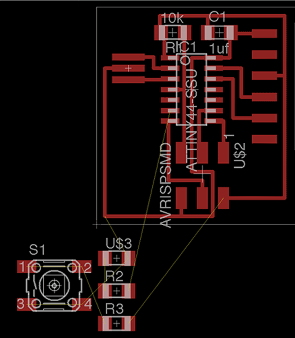
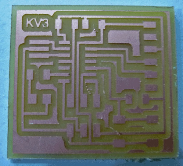
This is my finished layout:
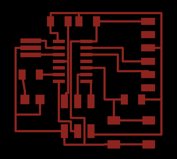
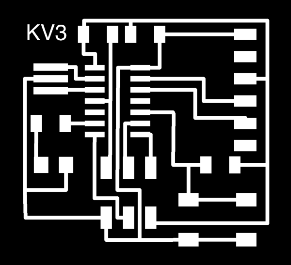
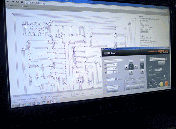
After making the layout you have to export a png file to be able to mill the traces on a copper board. And it has to be in black and white so the machine is able to recognize the traces and the excess material. Here is a comparisson between the traces before exporting it and after ina a png:
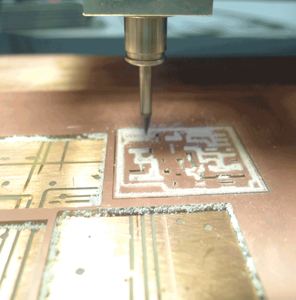
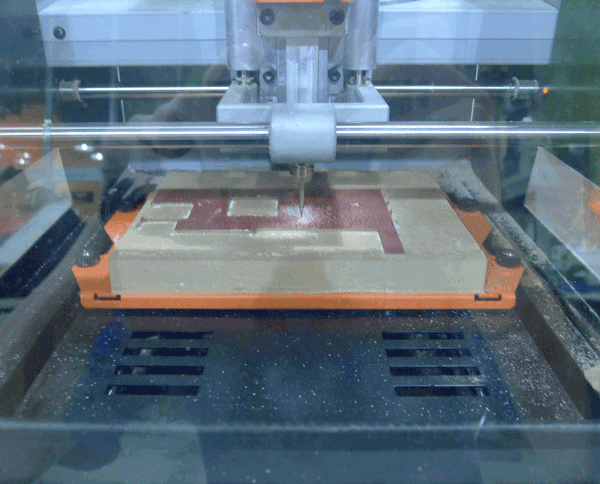
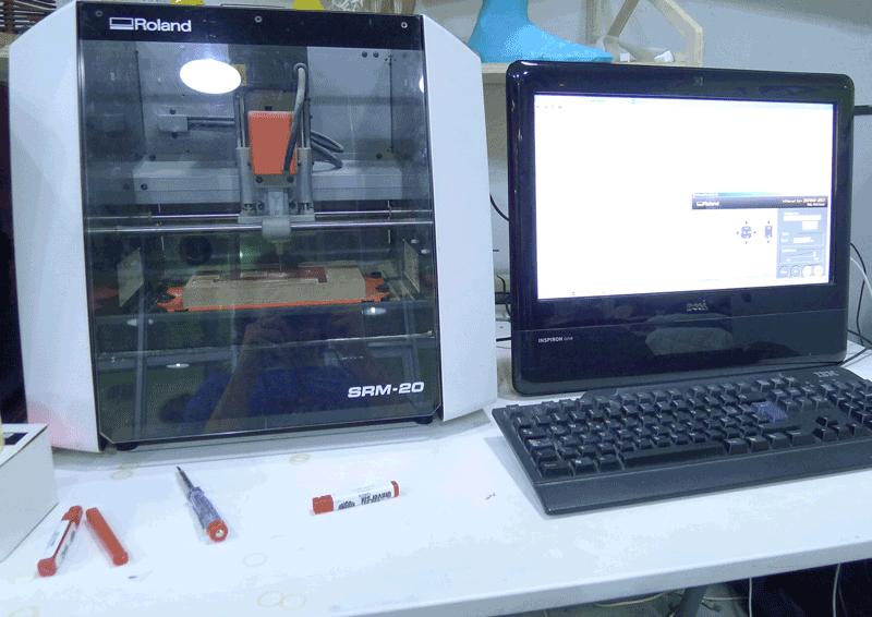
Milling the board
As we did in week 4 making the fabISP this is the same process but with a different design. We prepare our file the same way as we did the last time:
1· Prepare the file in fab modules
2· Place our copper board correctly on the modela
3· Put the correct mill bit in for milling the traces
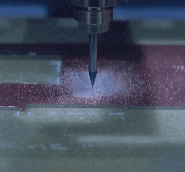
4· Mill the traces on the board
5· Change bits from 1/64 to 1/32
6· Mill the cutout of the board
Stuffing the board
When all of this is complete we have to make sure we have all the correct components to stuff, wich are:
· 6-pin programming header: for programming the board
· Micro controller: attiny44A.
· FTDI header
· Capacitator 1uf
· 20MHz resonator
· Resistor (value 10k)
· Button (OMERON switch)
· LED (Light Emitting Diode)
· Resistor (value 499 ohms)
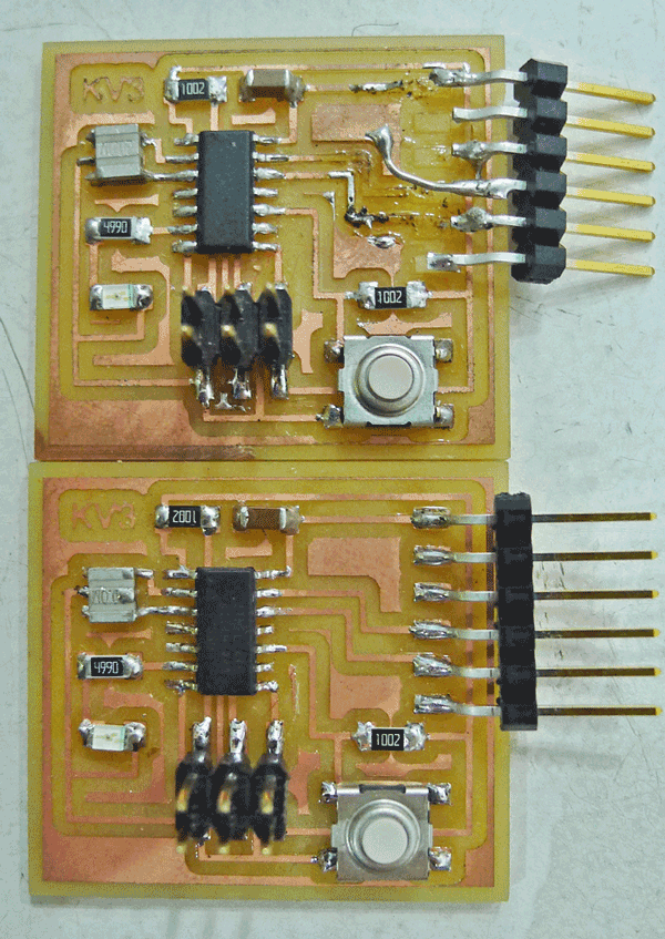
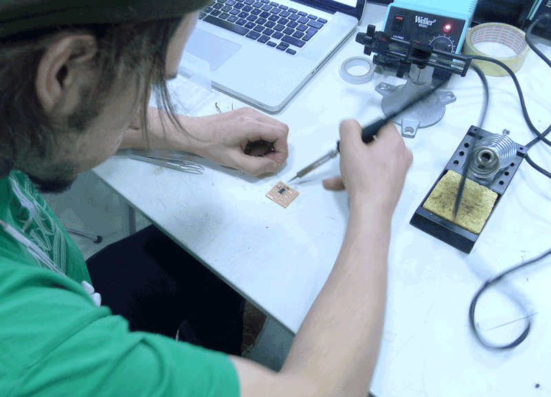
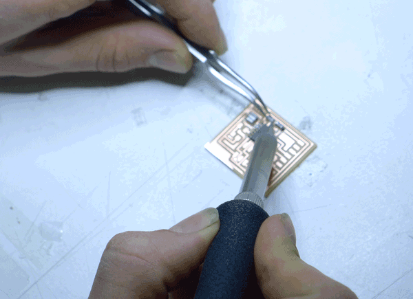
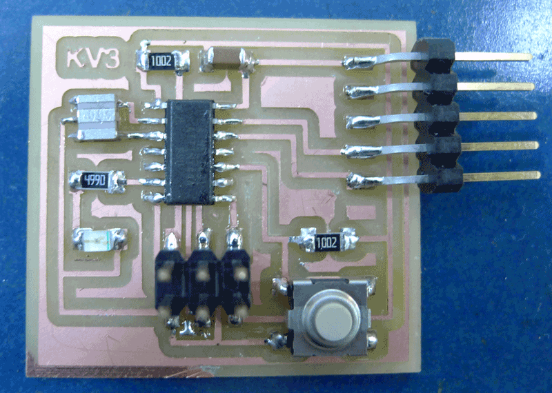
Once I had all these components it was time to start stuffing the board. Here are a couple of photos of the board and while stuffing it:
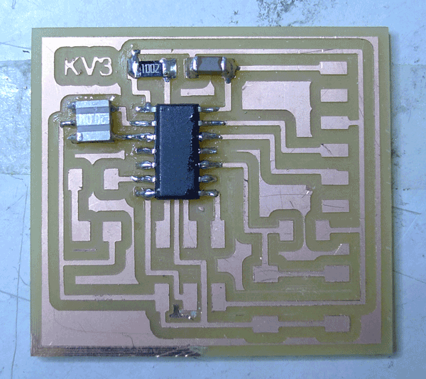
Finished board
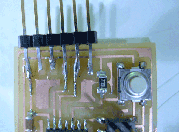
I wanted to start programming the board just after untill I realized that I soldered 5 conections instead of 6 on the FTDI heade traces. I tried to desolder the one that was originally stuffed but unfortunetley I broke off the connections to the board so I had to manually resolder the header to the traces that remaied behind. This is the board after this:
When programming it it worked perfectley, but after a couple of times of connecting and reconnecting the ftdi cable it broke again so i decided to redo the whole board from scratch. This time i used a different machine that was much better miller and much faster. Here are a couple of images of the second time:
This is the board that came out of the machine:
Here is a photograph of the comparison between both boards: