Week 08
Electronics Production
PCB Toolpath Generation, CNC Milling, Soldering, Testing, and Programming
1. Checklist
- ✅ Linked to the group assignment page
- ✅ Documented the PCB toolpath generation process
- ✅ Documented PCB milling using a CNC router
- ✅ Stuffed and soldered the board
- ✅ Checked continuity and possible short circuits
- ✅ Programmed and tested the board
- ✅ Included the source code
- ✅ Included a hero shot / final functional evidence
- ✅ Reflected on the process and problems found
2. Group Assignment
For the group assignment, the lab characterized the design rules for the in-house PCB production process and documented the machine settings used for PCB fabrication. This is important because the limits of the process define the minimum trace width, clearance, tool diameter, cutting depth, and general reliability of the fabricated board.
3. Introduction to Electronics Production
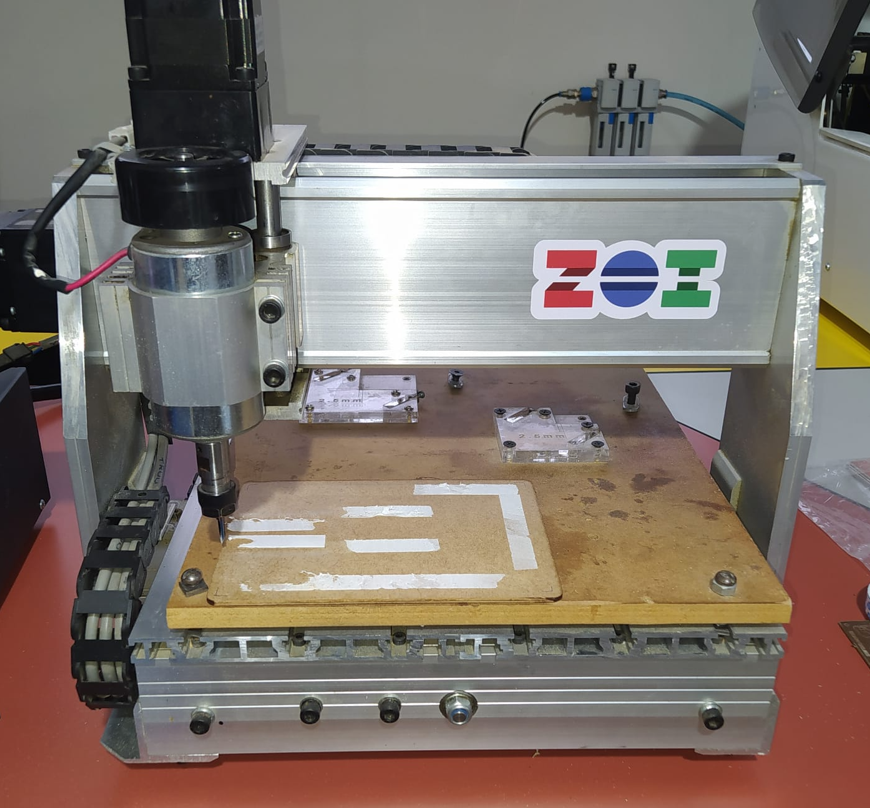
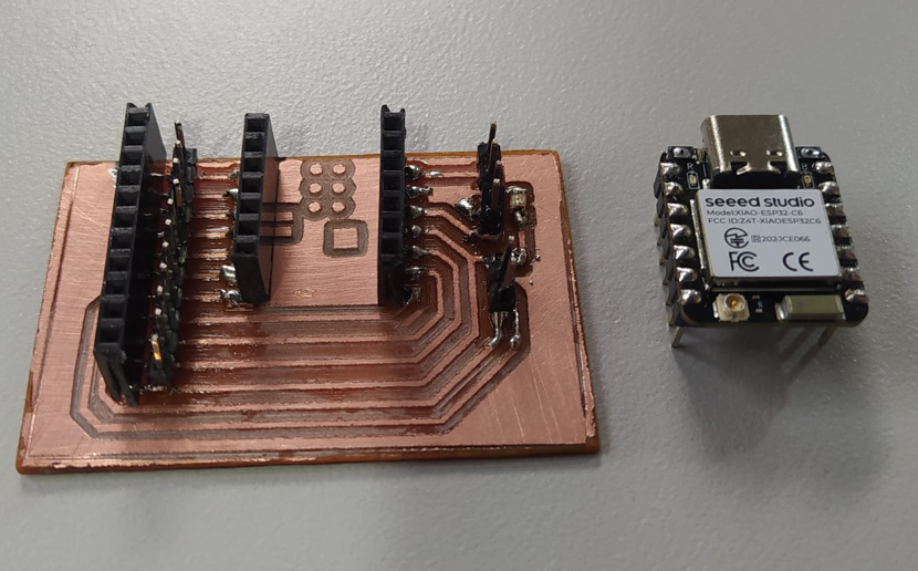
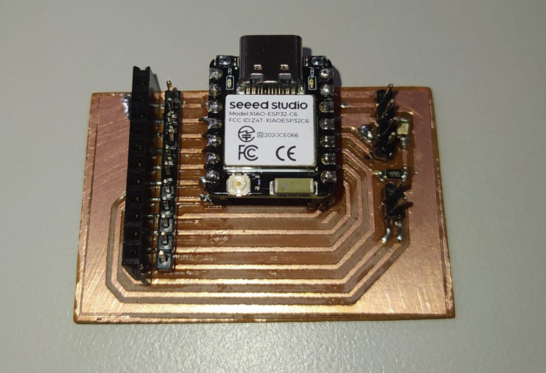
Electronics production is the process of transforming a digital PCB design into a real physical board. In this assignment, the objective was to make and test a microcontroller development board that I had previously designed. The board is based on the XIAO ESP32-C6 and works as a small trainer board to access the XIAO pins more easily and test an onboard indicator LED.
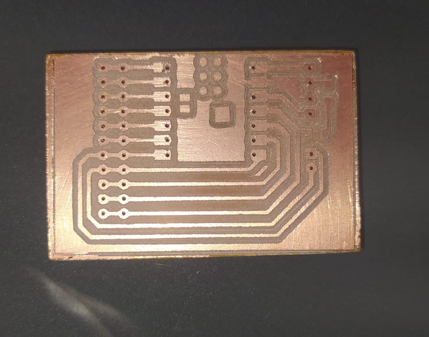
For this process, I used a CNC router to mechanically remove the copper around the traces. This method is commonly used in Fab Labs because it allows rapid prototyping of single-sided PCBs without using chemical etching. The machine removes copper by following a toolpath generated from a black and white PCB image.
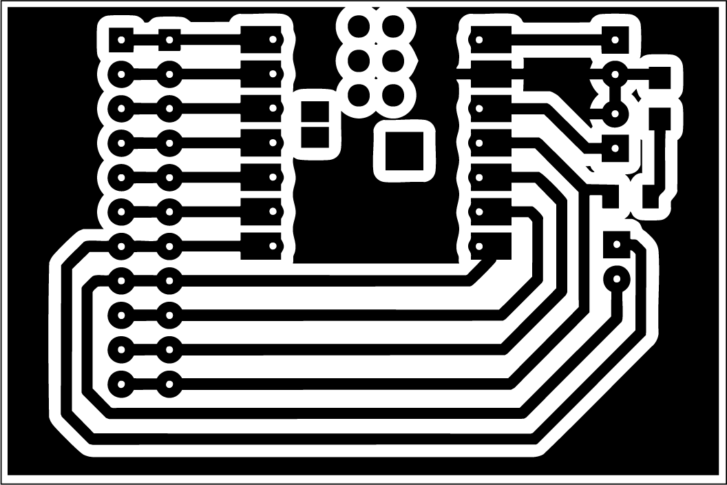
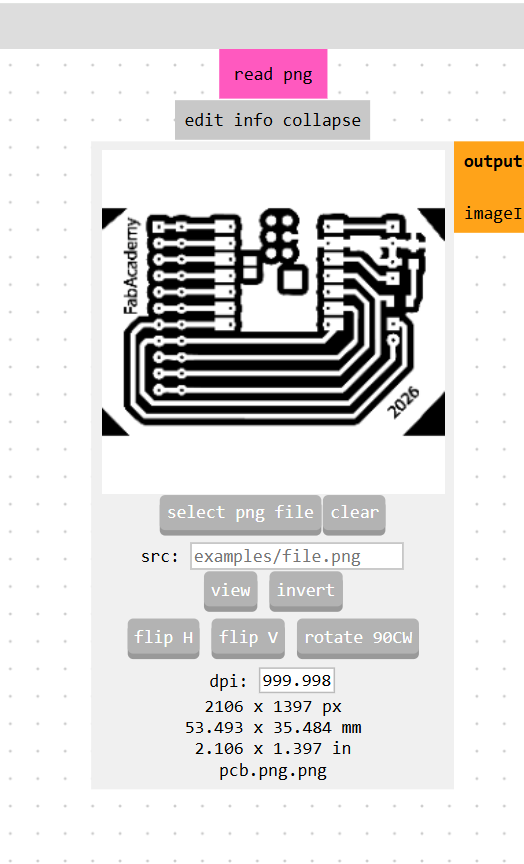
4. PCB Design Export from EasyEDA
The PCB design was previously created in EasyEDA. For fabrication, the important step was exporting a clean PNG image of the board at good resolution. The image was exported at 500 dpi with a white background and black copper geometry.
For this export, only the fabrication-relevant layers were kept active: traces, pads, drills, and board outline. The rest of the layers were disabled because they are not needed for the toolpath generation process. This creates a clean image that can be interpreted by the CAM workflow.
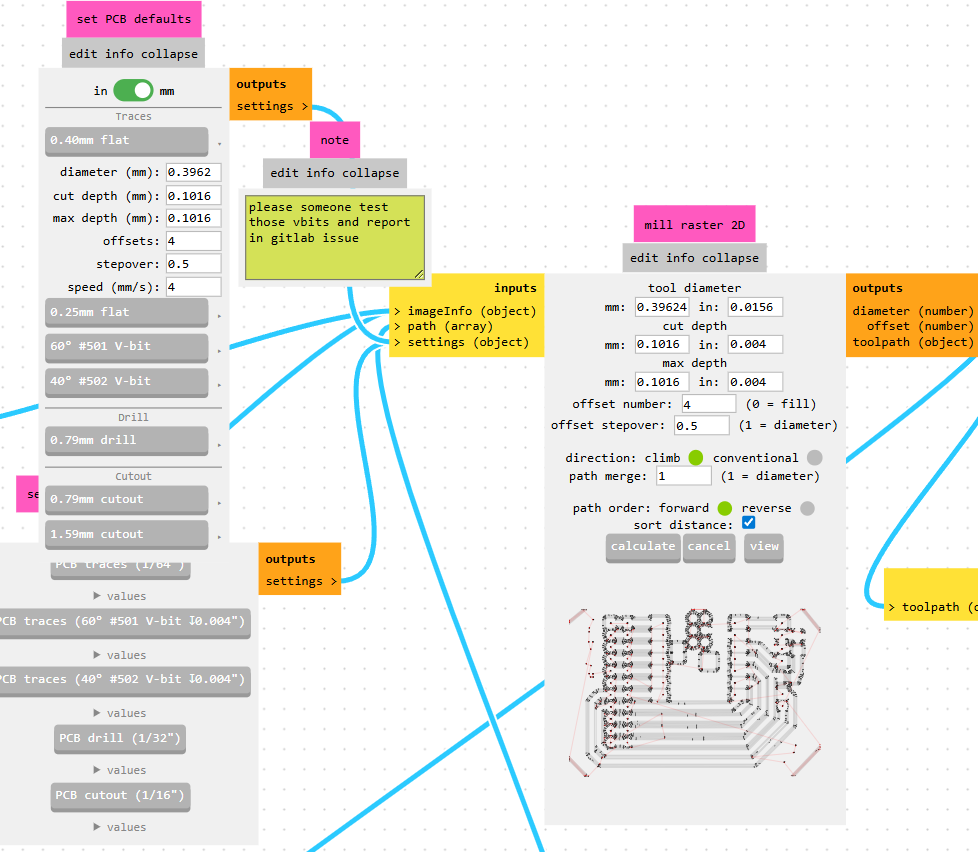
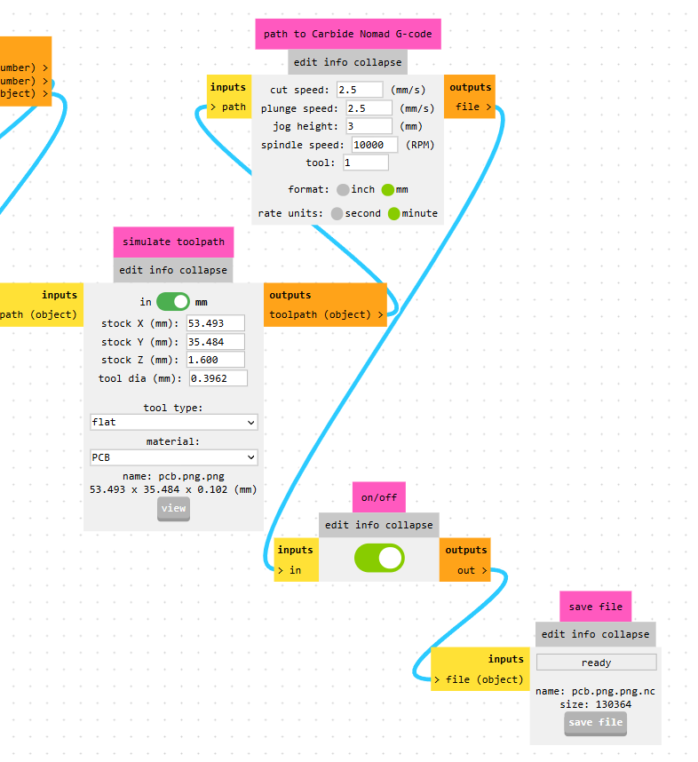
5. Toolpath Generation with Mods
To generate the toolpath, I used Mods, a browser-based modular tool developed in the MIT Center for Bits and Atoms ecosystem. Mods works through connected blocks, where each block receives data, processes it, and sends the result to another block. This makes the workflow very flexible because it can connect image inputs, machine settings, path generation, simulation, and output files.
Mods includes several ready-to-use workflows for digital fabrication. In this case, I searched for PCB and opened the Carbide Nomad PCB workflow. This workflow provides routes for different input formats, including PNG and SVG. For my board, I used the PNG route because my PCB was exported as a black and white raster image.
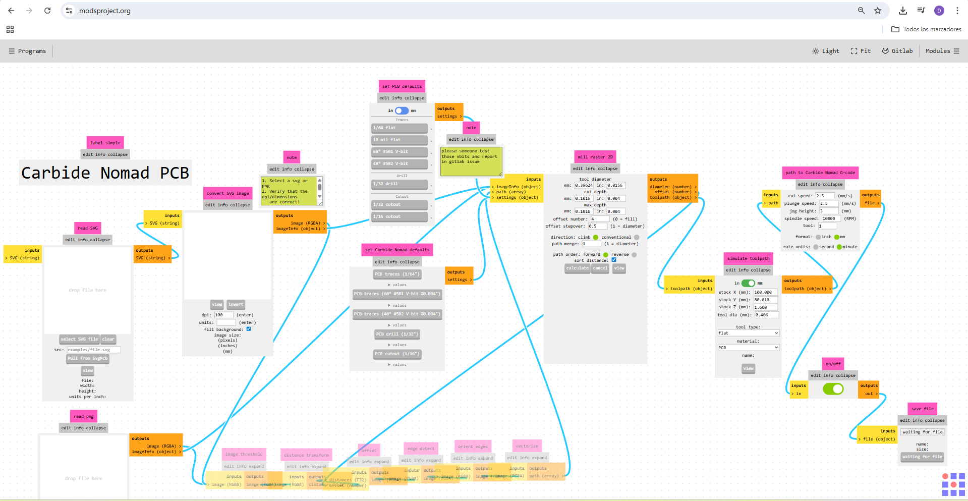
In the workflow, I selected millimeters as the working unit and configured the tool as a V-bit equivalent option using 0.4 mm flat. After that, I calculated the 2D raster toolpath to generate the machining path.
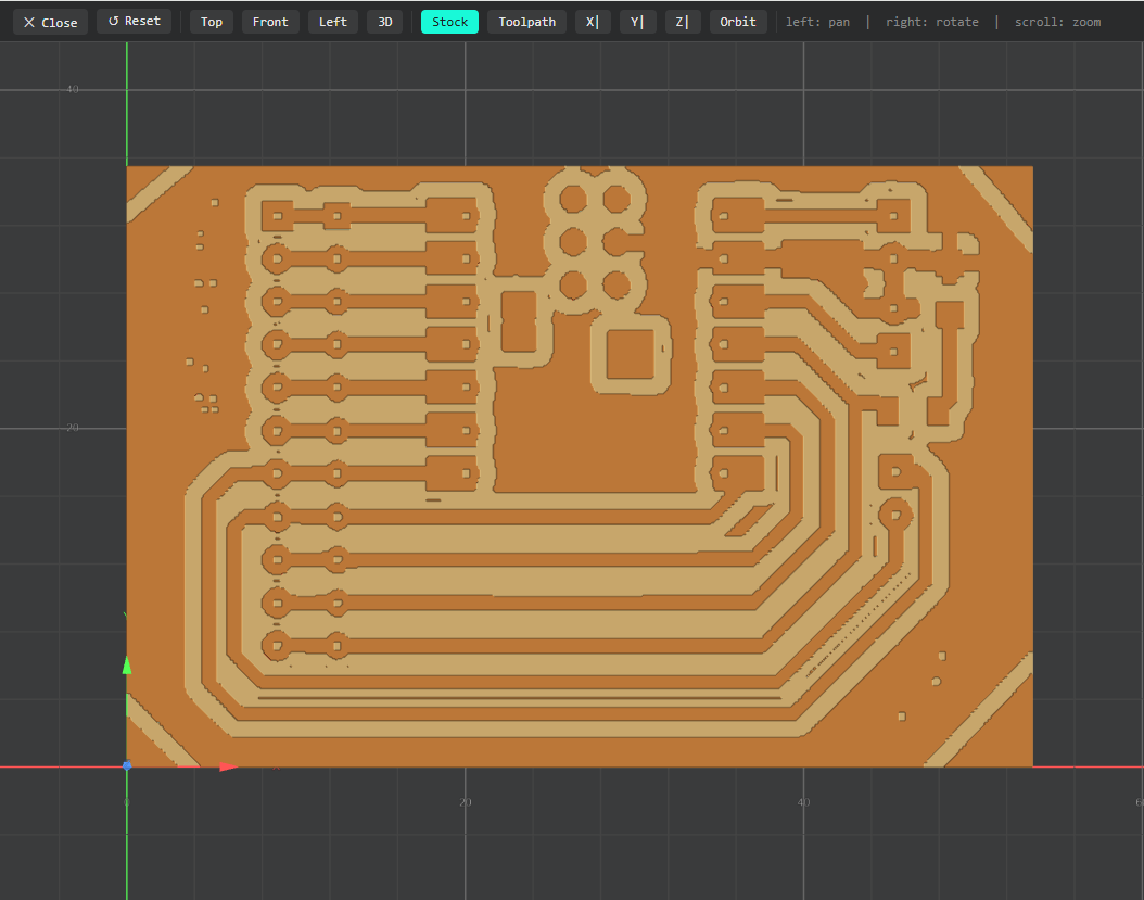
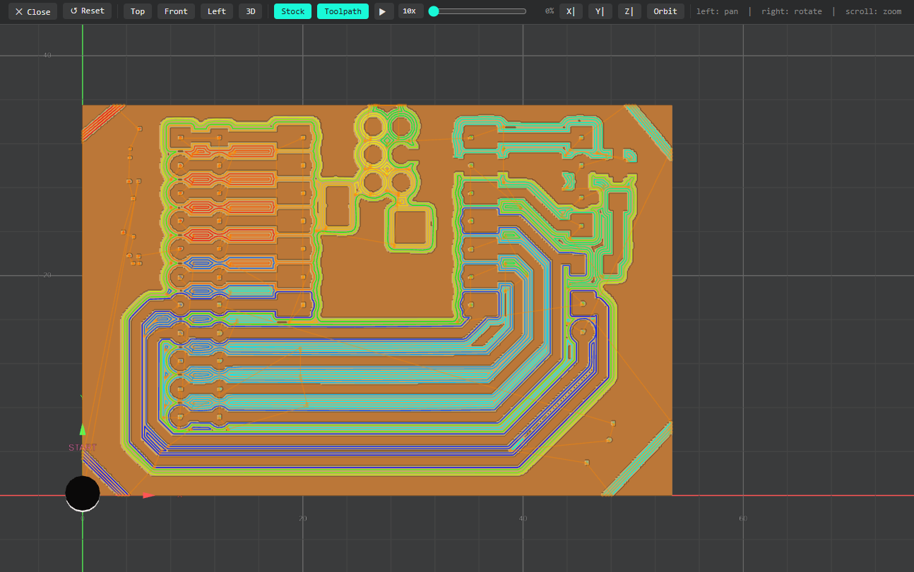
6. Toolpath Simulation
After calculating the raster toolpath, Mods automatically opened a simulation window. The simulation is useful because it allows checking how the PCB will look after milling before sending the job to the machine.
7. G-Code Generation
Once the simulation was checked, the final step in Mods was to generate the machine code. The output file was generated as a .nc file, which was later imported into the CNC control software.
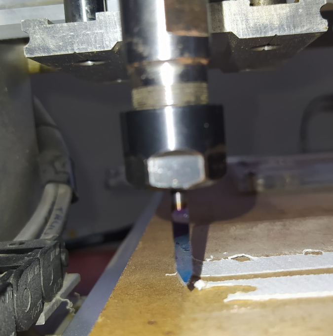
8. PCB Milling Tool
For the milling process, I used a 45° V-bit. This type of tool is common for PCB milling because it can create narrow isolation paths around the traces. Before using the tool, it is important to check that the tip is in good condition, because a damaged tip can affect the trace quality and cause broken or irregular paths.
PCB milling tools are very sensitive to the Z height. If the tool cuts too deep, it can remove too much copper and damage thin traces. If it cuts too shallow, the copper may not be fully isolated. For that reason, Z calibration is one of the most important parts of the fabrication process.
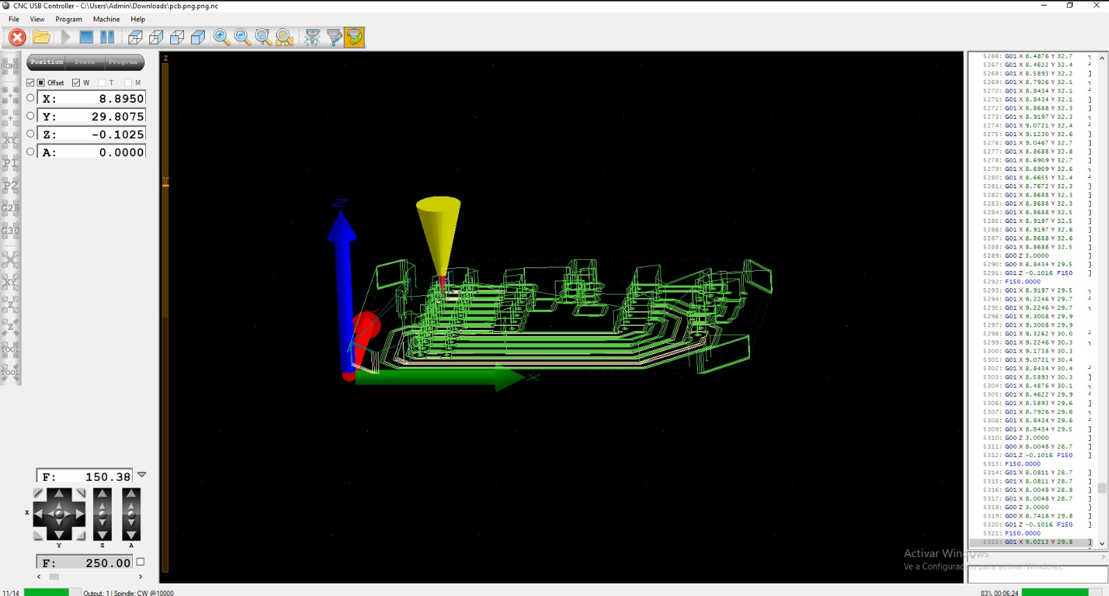
9. CNC USB Controller Setup
The CNC machine was controlled using CNC USB Controller. In this software, I imported the generated NC code, reviewed the toolpath simulation, and set the work zero for X, Y, and Z.
The material used was a single-sided copper-clad board, commonly known as baquelite board. It has copper on only one side, which is removed by the tool to isolate the traces. The board was fixed to the CNC bed using double-sided tape to prevent movement during machining.
The XY zero was placed at the lower-left corner of the board, and the Z zero was taken from the top copper surface. The cutting depth configured in Mods was 0.1016 mm. Before cutting the real board, I ran an air test with a higher Z position to verify that the coordinate translation and toolpath behavior were correct.
10. PCB Milling Process
After verifying the air test and calibrating the Z height on the material, I started the machining process. During milling, the CNC router removed the copper around the traces, leaving the conductive paths isolated.
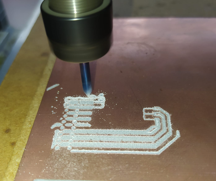
Once the milling process finished, the PCB was removed from the CNC bed. I used a hard-bristle brush to clean the surface and remove small copper particles or imperfections left by the milling process. After cleaning, I performed a first visual inspection to check that the traces were correctly isolated and that no visible bridges remained between copper areas.
11. Components and Board Stuffing
The board was designed as a small XIAO trainer board. Its purpose is to make the XIAO ESP32-C6 pins easier to access, provide male and female header options for jumper connections, and include a simple onboard LED indicator for testing.
| Component | Description | Package / Value |
|---|---|---|
| XIAO ESP32-C6 | Main microcontroller module | Module |
| Red LED | Indicator LED for functional testing | SMD 1206 |
| Resistor | Current-limiting resistor for the LED | SMD 1206 / 499 Ω |
| Female headers | Used to mount the XIAO without soldering it permanently | 2.54 mm pitch |
| Male headers | Used to connect jumper wires and access GPIO pins | 2.54 mm pitch / from 40-pin strip |
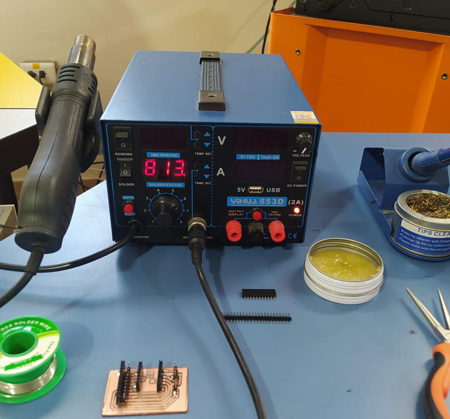
For soldering, I used a soldering station with adjustable temperature, a fine tip for SMD components, solder paste, and 0.8 mm solder wire with 99.3% Sn and 0.7% Cu. For small boards, it is important to use a clean fine tip, an appropriate temperature, and enough flux or solder paste to create clean joints without overheating the pads.
Traditional solder alloys often contain lead, but lead-free solder is commonly used for safer and more environmentally responsible work. Lead-free solder usually requires slightly higher temperature and good technique to obtain clean solder joints.
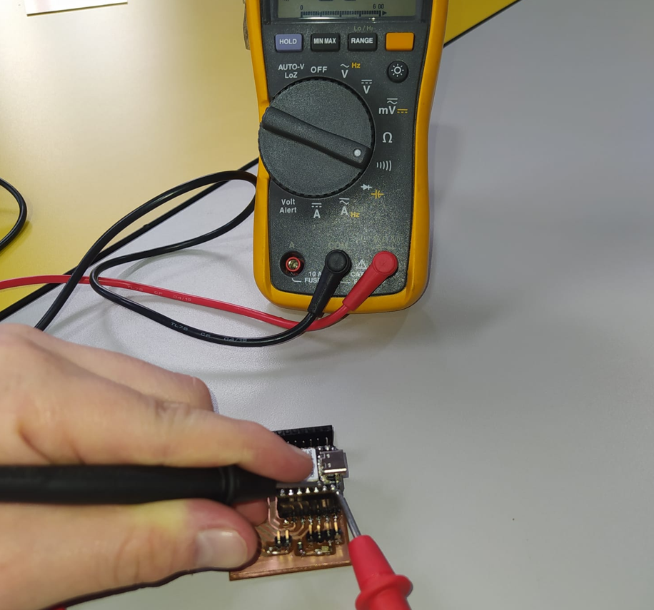
12. Continuity Testing
Before powering or programming the board, I checked the PCB using a Fluke 117 multimeter in continuity mode. This step is essential because a short circuit between power rails could damage the XIAO, the computer USB port, or the board itself.
I first verified that there was no continuity between 5V and GND, between 3.3V and GND, and between the different power rails. After that, I checked that the intended connections had continuity between the traces and the soldered components.
| Test | Expected Result | Purpose |
|---|---|---|
| 5V to GND | No continuity | Verify that the 5V rail is not shorted to ground |
| 3.3V to GND | No continuity | Verify that the 3.3V rail is not shorted to ground |
| 5V to 3.3V | No direct continuity | Check that both power rails are not accidentally bridged |
| LED trace and resistor path | Continuity where designed | Verify the intended signal path for the LED test |
| Header pins | Continuity according to schematic | Confirm that pin extensions are correctly connected |
13. Programming and Functional Test
After verifying the continuity of the board and confirming that there were no visible shorts, I programmed the XIAO ESP32-C6 using the Arduino IDE. The objective of the test was to blink the onboard LED connected to pin D10.
#define LED_PIN D10

void setup() {
  pinMode(LED_PIN, OUTPUT);
}

void loop() {
  digitalWrite(LED_PIN, HIGH); // Turn LED on
  delay(1000);

  digitalWrite(LED_PIN, LOW);  // Turn LED off
  delay(1000);
}
The LED blinking test confirmed that the board was successfully fabricated, soldered, powered, and programmed. This is the basic functional validation of the XIAO trainer board.
14. Problems and Fixes
During this process, the most critical points were related to Z calibration, trace isolation, soldering quality, and continuity verification. PCB milling requires very precise Z height because the copper layer is thin and small changes in depth can affect the final trace width.
- The Z height had to be checked carefully before cutting the real board.
- An air test was used before milling to confirm the toolpath behavior.
- The board was fixed with double-sided tape to prevent movement during machining.
- After milling, the board was cleaned with a hard-bristle brush to remove copper debris.
- Continuity was checked before connecting power to avoid damaging the XIAO.
- Solder bridges were visually inspected and checked with the multimeter.
15. Reflection
- This assignment helped me connect electronics design with physical electronics production. Designing a PCB is only one part of the process; making it real requires toolpath generation, machine setup, milling, soldering, inspection, and testing.
- One of the most important steps was checking continuity before powering the board. This prevents short circuits between 5V, 3.3V, and GND that could damage the microcontroller or the computer.
- I learned that Z calibration is critical in PCB milling. A small error in height can make the tool cut too deep, damage traces, or fail to isolate the copper correctly.
- The air test was useful because it allowed me to verify the toolpath movement before touching the copper board. This reduces the risk of wasting material or breaking the tool.
- Good fixturing is essential. Using double-sided tape helped keep the copper board flat and stable, which is very important for consistent milling depth.
- Soldering SMD components requires patience, a clean fine tip, correct temperature, and good control of the solder amount. Too much solder can create bridges, while too little solder can produce weak connections.
- It is important not to keep the soldering iron on the pads or components for too long. Excess heat can lift copper pads, damage traces, or burn small SMD components.
- Working with soldering tools also requires safety awareness. The soldering iron reaches high temperatures, so care is needed to avoid burns and to keep the work area organized.
- The visual inspection after milling and after soldering was very useful. Many problems can be detected early by checking trace separation, solder bridges, component orientation, and pad quality.
- The final LED test was simple but important because it confirmed the complete workflow: the design was exported, milled, soldered, powered, programmed, and tested successfully.
- This board is useful for future assignments and for my final project because it works as a small XIAO trainer board, making the microcontroller pins easier to access during prototyping.
- Overall, this week showed me that electronics production is a process where small details matter. A good result depends on design quality, correct machine configuration, careful soldering, and systematic testing.