Week 06
Electronics Design
PCB Design, Electrical Measurement, PWM Analysis, and Oscilloscope Practice
1. Checklist
- ✅ Linked to the group assignment page
- ✅ Designed an electronic board using EasyEDA
- ✅ Documented the schematic and PCB workflow
- ✅ Exported manufacturing and editable files
- ✅ Measured board voltages using a multimeter
- ✅ Analyzed digital signals and PWM with an oscilloscope
- ✅ Included reflections about the assignment
2. Group Assignment
For the group assignment, the lab characterized and analyzed electronic behavior using measurement instruments such as the multimeter and the oscilloscope. This included observing voltage levels, signal behavior, and practical measurements on a microcontroller platform.
3. Introduction to Electronics Design
Electronics design is the process of creating a circuit that defines how electrical components interact to perform a specific function. In this week, the work included both the digital design of a PCB and the practical analysis of electrical behavior using laboratory instruments.
Some fundamental concepts are essential before starting the design and testing process. Voltage is the electrical potential difference that drives current through a circuit. Current is the flow of electric charge through conductors. Resistance limits the flow of current, and power is the rate at which electrical energy is transferred.
A simple and useful relation between these variables is commonly explained through Ohm’s Law triangle: voltage, current, and resistance are directly related by the expression V = I × R. In practical terms, this relationship helps determine how a resistor affects the current passing through a load such as an LED.
In this assignment I worked with direct current (DC), which is the type of current delivered by USB power and by the regulated lines used by the XIAO board. This is different from alternating current (AC), where voltage changes direction periodically.
4. Electronics Design Software
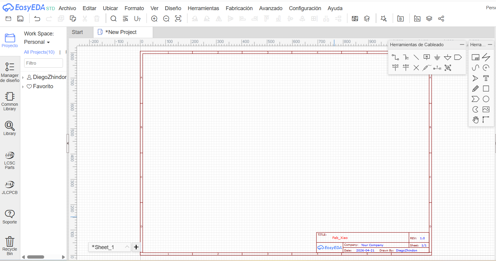
For the PCB development of this week, I used EasyEDA Standard Version in its online environment. EasyEDA is an electronic design automation platform that allows the complete workflow for board development inside the same software environment.
With EasyEDA, it is possible to create the schematic, search and place components from libraries, assign footprints, generate the PCB layout, verify component positions in 3D, and export manufacturing files such as Gerber, SVG, PDF, and editable project files.
One of its strengths is that the schematic and the PCB remain linked, so after defining the circuit connections, the board layout can be generated while preserving the same logical structure.
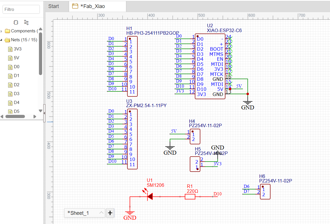
5. Schematic Design
The schematic is the first formal step in the electronics workflow. It defines the logical electrical relationships between all components, independent of their physical position on the final PCB.
5.1 Component Library
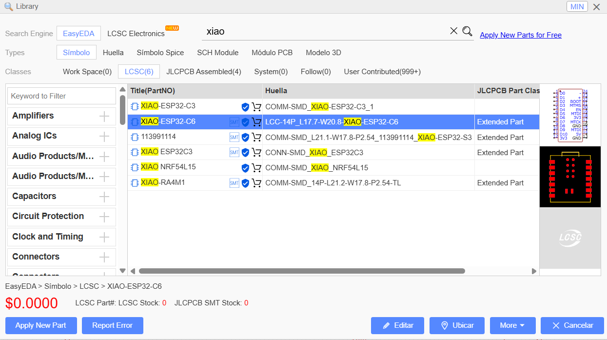
EasyEDA provides an integrated library that includes symbols, footprints, and many predefined components. This made it possible to search and place the required elements directly in the workspace.
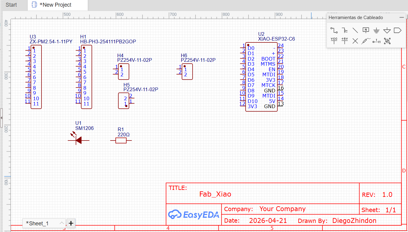
5.2 Components Used
| Component | Description | Package / Type |
|---|---|---|
| XIAO ESP32-C6 | Main microcontroller module used as the core of the board | Module |
| LED | Status indicator LED | 1206 |
| Resistor | Current-limiting resistor for the LED | 1206 / 220Ω |
| Male Pin Header | GPIO extension header | 11P / 2.54 mm |
| Female Pin Header | GPIO extension header | 11P / 2.54 mm |
| Male Pin Header | Auxiliary connection headers | 2P / 2.54 mm |
5.3 Components Placed in the Workspace
After selecting the required elements, all components were placed in the schematic workspace to begin the electrical definition of the board.
5.4 Connections and Labels
The circuit connections were defined using both wires and signal labels. Instead of relying only on long direct wires, I used net labels to keep the schematic cleaner, reduce visual clutter, and simplify the reading of the design.
Another important point is that unused pins should not remain ambiguous. In the schematic, pins that were intentionally left unconnected were marked using the No Connect flag. This avoids false connection errors and improves design clarity.
The GND symbol was used as the common electrical reference for the board. Ground is fundamental because it defines the zero-volt reference point of the circuit. All voltage measurements are made relative to that reference, which is why connecting the measurement instruments correctly to GND is essential.
6. PCB Design
After verifying that the schematic was complete and electrically consistent, the project was transferred to the PCB layout environment. This stage defines the physical position of each component and the actual copper traces that connect the circuit.
6.1 Initial PCB Layout
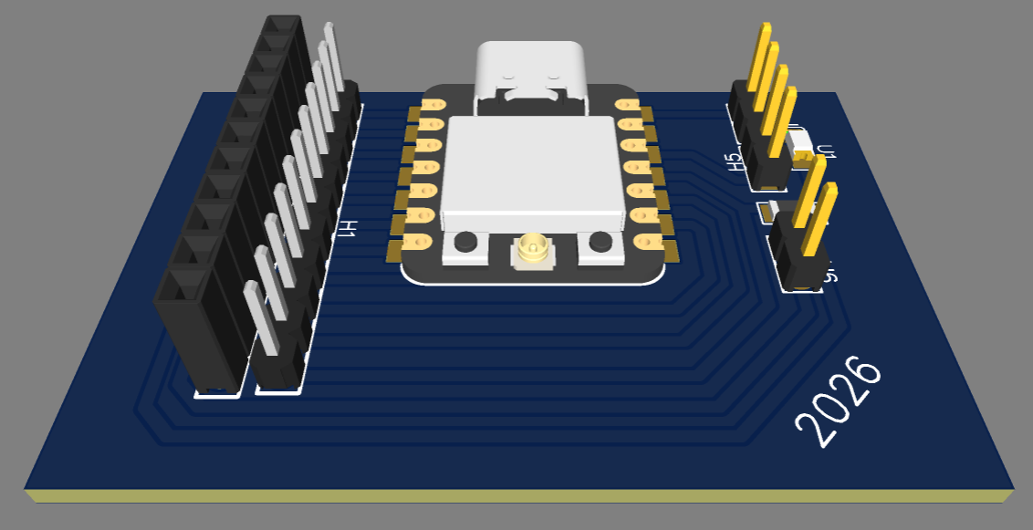
Once the PCB was generated from the schematic, the components were arranged manually according to their function and the desired geometry of the board. This step is important because good component placement makes routing easier and improves the usability of the final design.
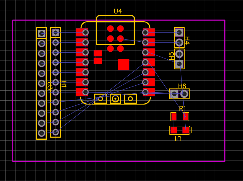
6.2 Routing
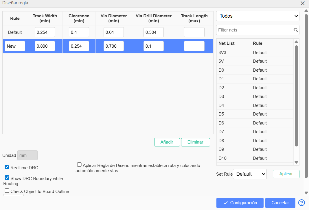
Routing is the process of creating the conductive paths that connect all components on the board. In this design, I used trace widths of 0.8 mm. This value provides a robust and easy-to-fabricate connection width for this board.
The board uses surface-mount components, which is common in compact PCB designs because it reduces overall size and supports organized routing around the board.
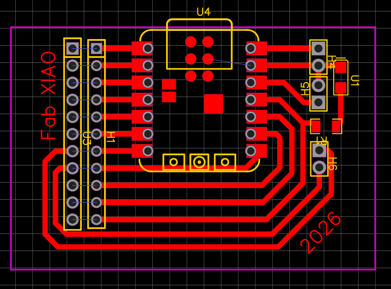
6.3 Ground Plane and Polygon Tool
After routing the signal traces, I used the polygon tool to generate a ground plane. A ground plane is useful because it creates a large common reference area, improves electrical stability, reduces noise, and can simplify the routing of return paths.
In this board, the ground plane was created with a clearance of 0.254 mm. Clearance is the minimum distance between the copper pour and the other traces or pads. It is important because it prevents unintended short circuits while allowing the polygon to fill the remaining copper area.
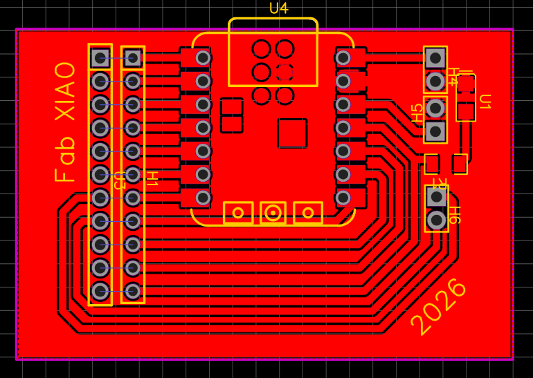
6.4 3D Visualization
EasyEDA includes a 3D viewer that allows checking the physical appearance of the board before fabrication. This is useful to confirm the component placement, general proportions, and the overall visual result of the design.
6.5 Fabrication Preview
EasyEDA also provides a preview of how the PCB would look in a professional fabrication process, including solder mask, plated holes, pads, and other manufacturing-level visual elements.
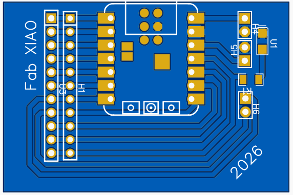
6.6 Monochrome Export for Alternative Fabrication
A monochrome exported version of the PCB was also generated, showing only the top view, holes, traces, and board frame. This kind of graphic output is useful for alternative fabrication processes such as milling, engraving, or other custom production methods.
In this type of image, the contrast is normally used to define what should remain as copper and what should be removed. In practical terms, the dark path areas represent the conductive geometry of the board, while the surrounding clear zones define the material to be isolated or removed depending on the fabrication workflow.
6.7 Design Rules and Criteria
The PCB design was not only defined by schematic connectivity, but also by a set of design rules based on electrical requirements and fabrication constraints. These rules ensure that the board is manufacturable using CNC milling and electrically reliable during operation.
| Design Parameter | Value | Technical Criteria |
|---|---|---|
| Operating Voltage | 3.3V / 5V | Defined by the XIAO ESP32-C6 logic levels and USB power supply |
| Maximum Current | 150 mA | Based on the expected load (DC motor), while sensors operate below 50 mA |
| Trace Width | 0.8 mm | Oversized relative to current requirements to improve mechanical robustness, ease of soldering, and ensure reliable CNC milling considering tool limitations |
| Clearance | 0.254 mm | Defined according to the milling tool diameter to prevent trace merging and ensure proper isolation between conductive paths |
| Ground Plane | Top layer polygon | Implemented to provide a stable reference, improve return paths, and reduce electrical noise, especially due to the presence of a DC motor |
| Component Placement | Functional grouping | Components were placed based on logical connectivity to minimize trace length, simplify routing, and improve overall board organization |
| Mounting Strategy | Top layer (SMD + THT) | Surface-mount components were used for compactness, while the XIAO module was placed on the top layer using through-hole headers for accessibility and modularity |
| Manufacturing Constraints | CNC Milling | All design rules were adapted to the limitations of subtractive fabrication, including tool diameter, trace spacing, and achievable resolution |
These design decisions were based on both electrical performance and fabrication constraints, ensuring that the board can be reliably manufactured and operated under real conditions.
6.8 Downloadable Design Files
After completing the design, I exported the main files needed for documentation, fabrication, and future editing.
12. Reflection
- This assignment helped me understand electronics design as a complete workflow rather than as an isolated PCB drawing task. I worked through the full process: selecting a design platform, understanding the role of the schematic, organizing component relationships, transferring the project to the PCB environment, defining routing decisions, and finally validating part of the circuit behavior with real measurements.
- One of the most important lessons was the difference between the logical representation of a circuit and its physical implementation. In the schematic, the priority is electrical clarity: identifying signals, defining references, and making the functional intention of the circuit understandable. In the PCB stage, the priority changes toward physical order, spacing, manufacturability, and usability.
- Working in EasyEDA helped me understand the value of an integrated EDA environment. It was useful to have the component libraries, schematic editor, PCB editor, 3D visualization, and file export tools inside the same system. This made the workflow more efficient and also helped me see how schematic decisions directly affect the physical board.
- Another important reflection was the value of keeping the schematic visually clean and technically explicit. Using net labels instead of excessive crossing wires made the design easier to read and maintain. In the same way, adding no-connect flags to intentionally unused pins was important to avoid ambiguity and show that each unused connection had been considered, not forgotten.
- The board design stage made clear that component placement is not only an aesthetic decision. The location of the XIAO module, LED, resistor, and headers strongly affects trace organization, routing simplicity, and the final usability of the board. Good placement reduces unnecessary crossings, shortens paths, and produces a cleaner board that is easier to fabricate and understand.
- Trace design was also an important learning point. Choosing a 0.8 mm trace width was not arbitrary; it reflects a balance between mechanical robustness, ease of fabrication, and practical layout clarity. This week helped me understand that routing is not only about connecting pads, but about defining reliable conductive paths that must respect space, order, and manufacturing constraints.
- The use of a ground plane was one of the most relevant design concepts of the week. Before this assignment, ground could easily be understood only as a symbol in the schematic, but now it became clearer that ground also has a strong physical meaning in PCB layout. The polygon-based ground plane helps create a common reference area, improves electrical stability, supports return paths, and can reduce noise in practical implementations.
- Defining a clearance of 0.254 mm also reinforced the idea that PCB design must follow physical rules, not only visual logic. Clearance is essential because it protects the electrical isolation between copper areas and prevents unintentional shorts. This made me more aware that PCB design is strongly tied to manufacturing capability and board reliability.
- The 3D visualization and fabrication preview stages were more valuable than I initially expected. They helped confirm not only the physical appearance of the board, but also the practical coherence between footprint selection, component arrangement, and expected fabrication results. Seeing the board in 3D and in manufacturing view gave more confidence before exporting the final files.
- Exporting multiple fabrication formats also showed that one electronic design can support different production workflows. Gerber files are intended for standard PCB manufacturing, while SVG, PDF, and monochrome image exports can support documentation, vector editing, or custom fabrication methods. This helped me understand that documentation and fabrication outputs are also part of the design process.