The process
Group assignment
The brief for this week's group work was to characterise the design rules for our in-house PCB production process — the minimum reliable track width, the minimum trace-to-trace spacing, and the smallest isolation gap that our milling / vinyl-cutting setup could hold consistently. The full write-up was led by my colleague Aisha Alshehri and is documented there in detail.
What I took away for my own work:
- Track width — the group characterisation showed 0.5 mm as the reliable lower bound for our setup. That became the track-width setting I used in every PCB revision in KiCad through to the final project — narrow enough to fit dense routes around the ESP32-C3 footprint, wide enough that the mill (or the vinyl cutter, in the fallback path) reliably produced an unbroken trace.
- Trace spacing & isolation — anything below 0.4 mm risked bridging during milling or being torn during the copper-tape weed step. I kept clearance at 0.4 mm minimum in DRC throughout.
- Design-for-fabrication mindset — the level of detail the group spec asked for (per-process design rules, not just "what works on paper") was a real eye-opener. It's the same mindset I'd need if I ever moved my final project from one-off academy artefact toward a commercial product at scale.
Individual assignment:
Make and test an embedded microcontroller system that you designed. Because of the geopolitical situation in the Gulf region, our shipment was delayed and we did not get the copper-clad FR1 sheets to produce our PCBs, nor the milling bits we had requested. I started with vinyl-cut and 3D-printed PCBs. By Weeks 12–13 we started receiving the PCB stock and end mills.
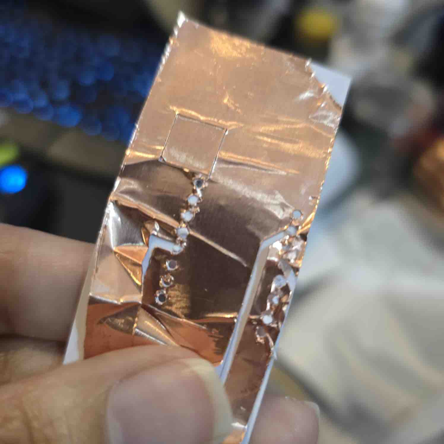
01: Vinyl PCB using copper tape
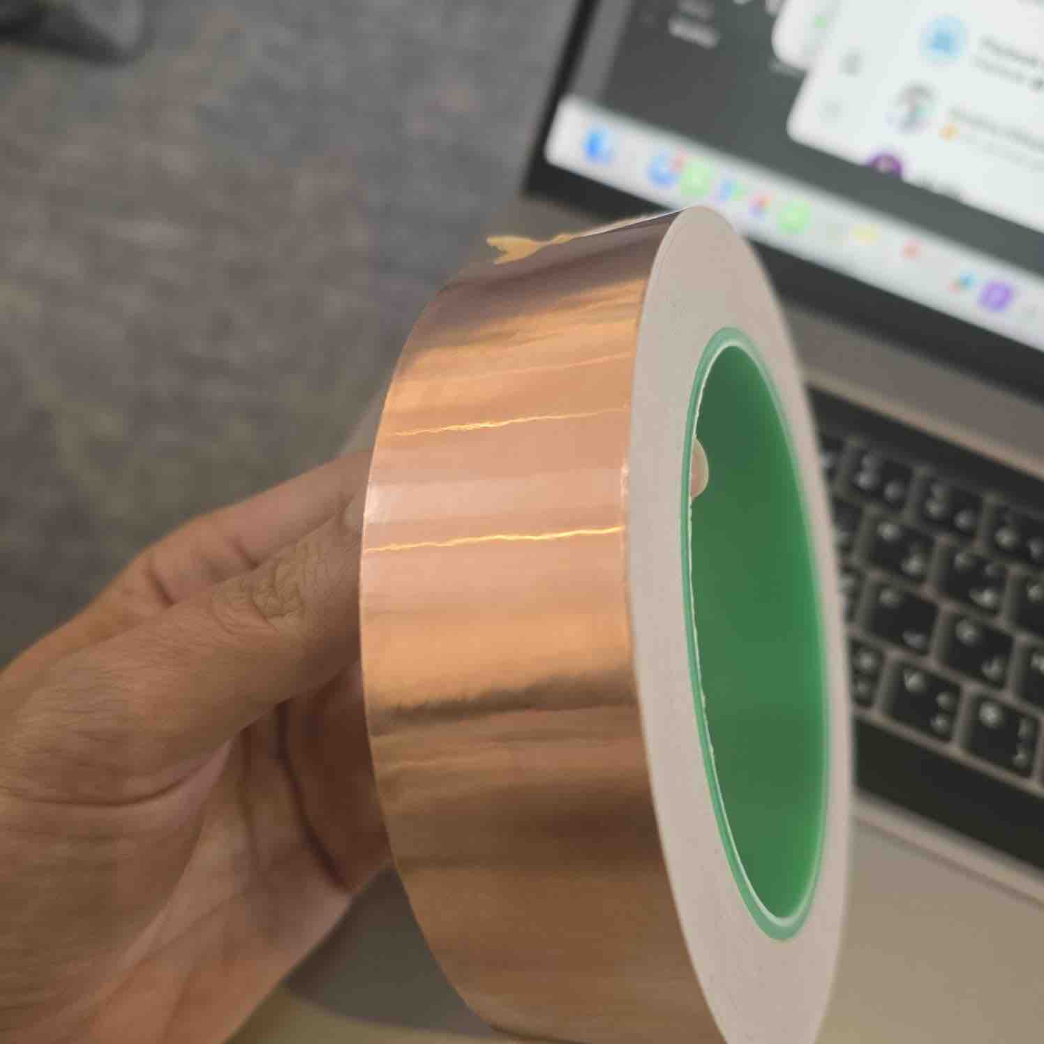
01 | I tried to use 1-inch copper tape to cut the main routes of my PCB
02 | I first had to redesign my circuit in KiCAD to fit 1 inch in height in the schematic editor
03 | Then I created the routes in the PCB Editor and made them 1mm thick to make sure the machine could cut them, and exported as SVG file
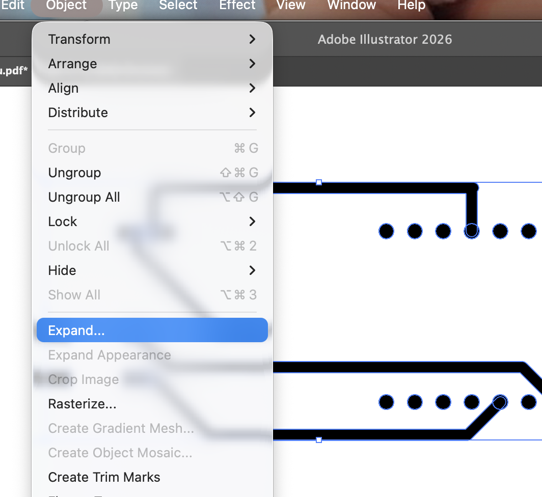
04 | Then I found that the routes were taken as strokes and not as shape paths, so I had to import the SVG into Adobe Illustrator and expand the lines into paths
05 | I tried to cut the circuit on a piece of tape, but it was a failure
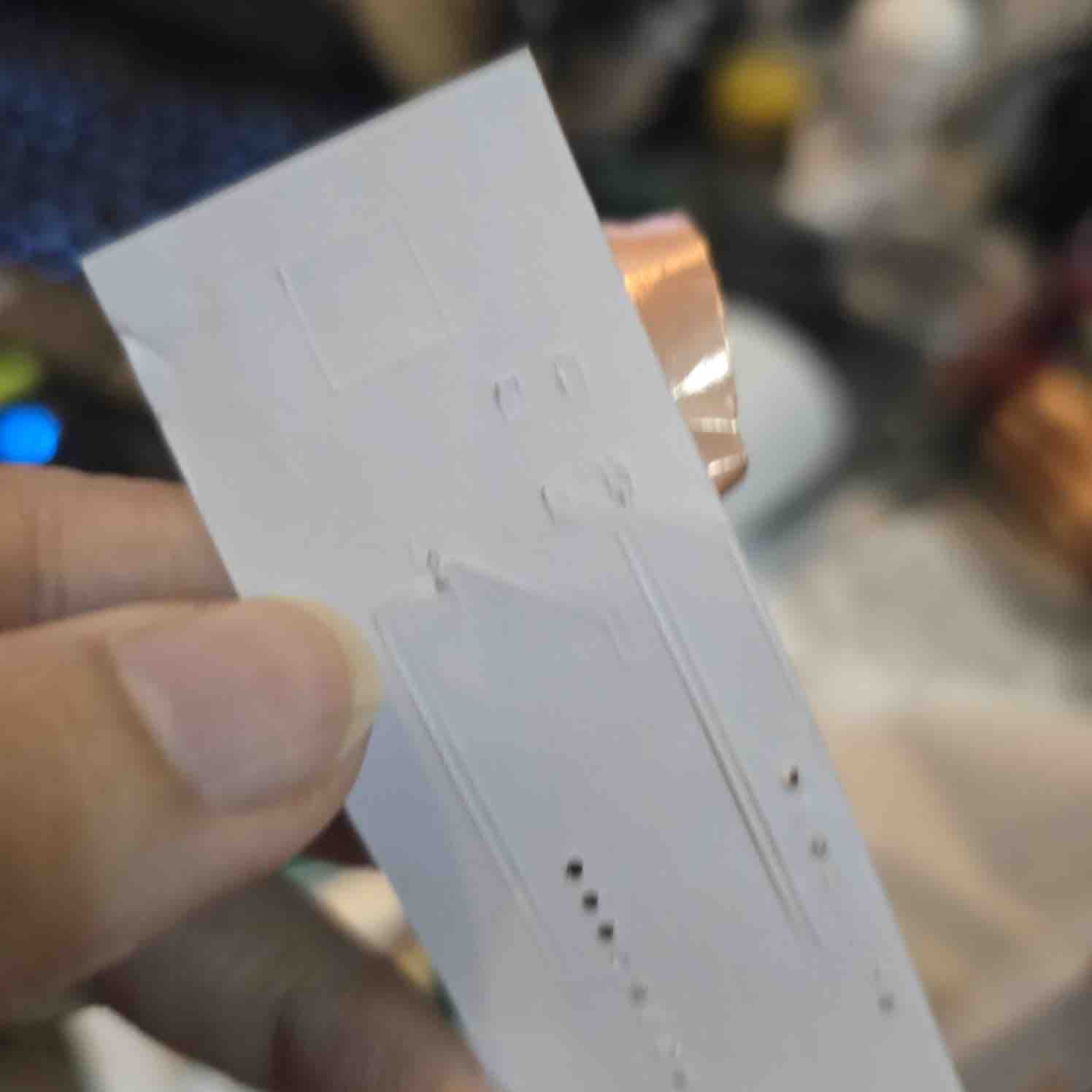
06 | The cutter went too deep and creased from the back of the tape
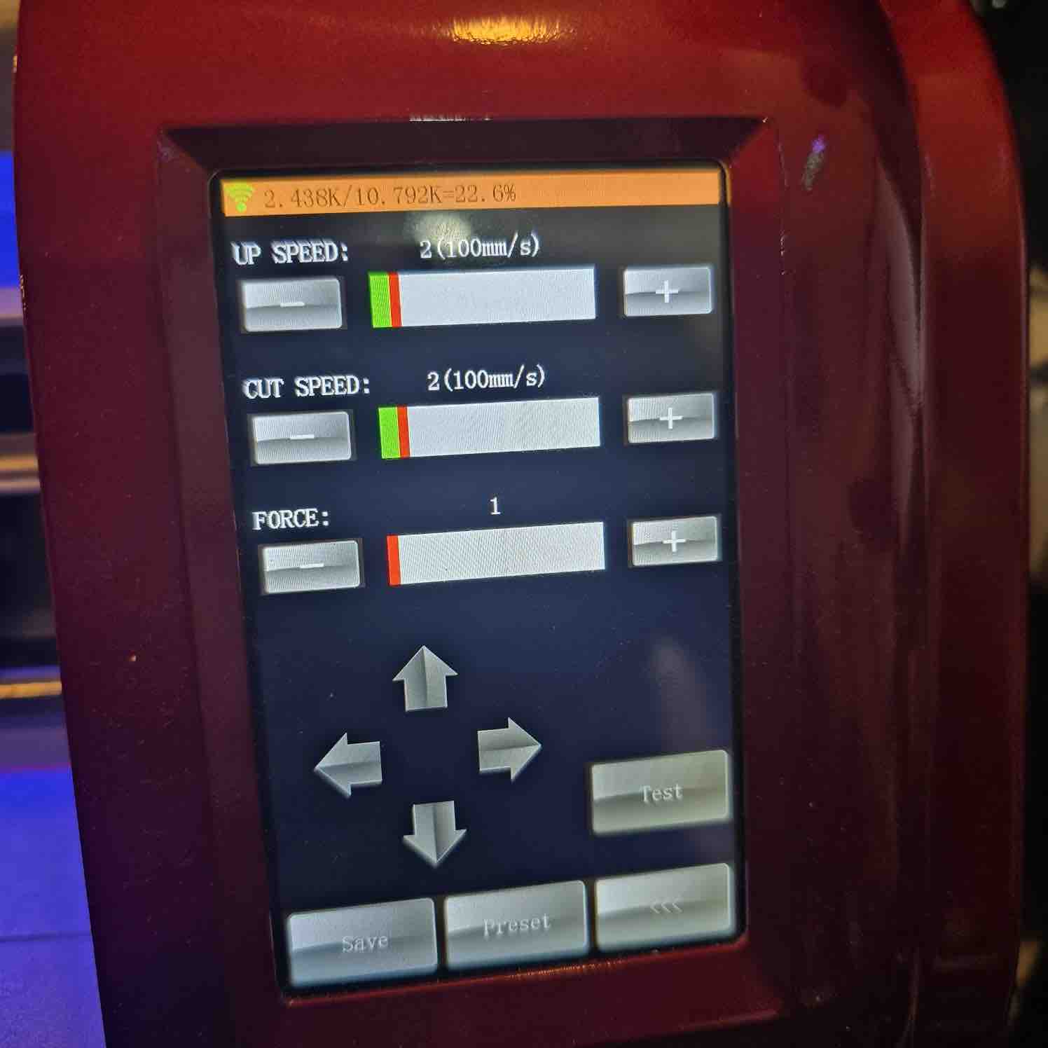
07 | Then I tried changing the settings, making the cut force the lowest and the speed the lowest
08 | The results were better than my first attempt
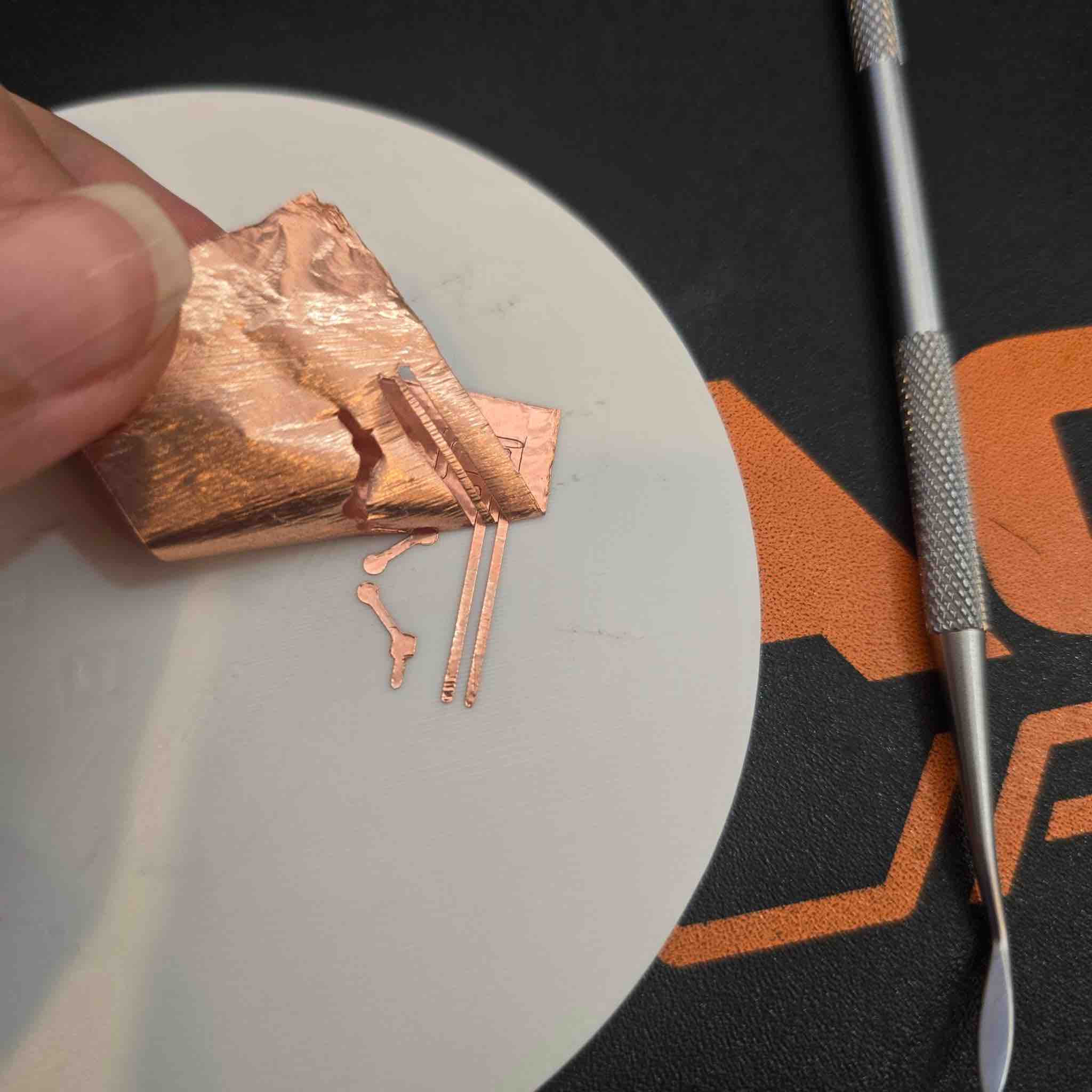
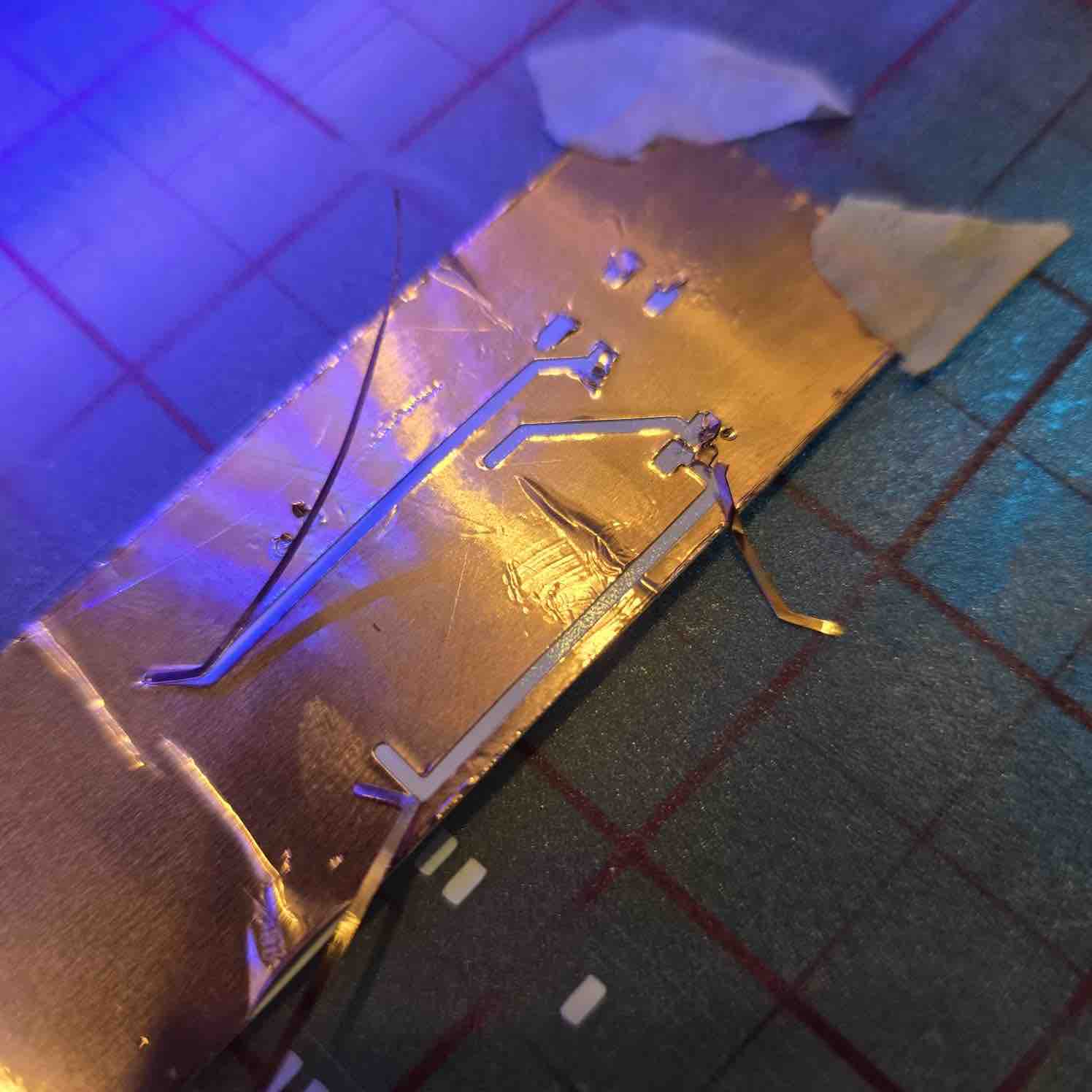
09 | I tried cutting the copper tape after placing it on a hard surface and got much better results
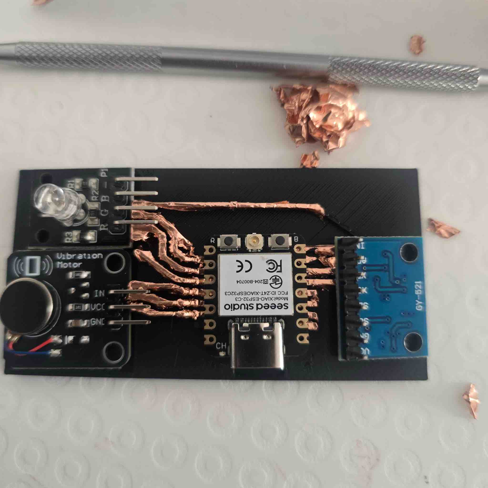
10 | I was able to solder different components, making a Vibration Motor module. The full process is documented in Week 10 — Output Devices.
- Feedback: Copper vinyl cut is not an easy process, but I believe it's worth making it work based on the examples I saw. I would love to create a cubic / 3D PCB one day ^_^
- Challenge: Balancing between the shapes the cutter can cut and the max size the PCB can be designed in is not easy — there is always a risk of creating short circuits, and it also makes soldering the parts to the board harder
02: 3D print PCB
01 | I tried the 3D PCB approach in Week 15 and documented it here in more detail.

02 | I first designed the PCB in KiCad, including all the components I'm planning to add in my final project. I set the track width to 0.8 mm to make sure the routes would be wide enough for the 3D printer.
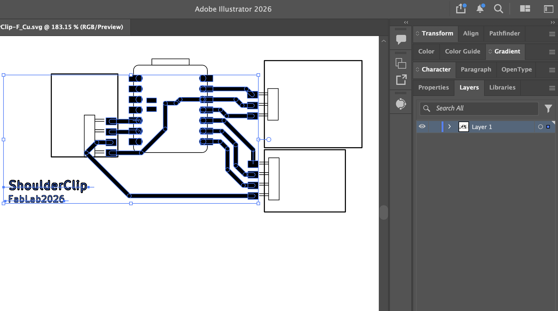
03 | I plotted the PCB design as an SVG file and imported it into Adobe Illustrator to convert the stroke lines into shapes.
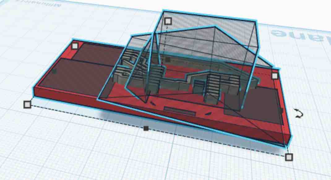
04 | I imported the SVG file into TinkerCAD and started working on it. I extruded the routes, then added hollow shapes to reach my final 3D-printed PCB design.
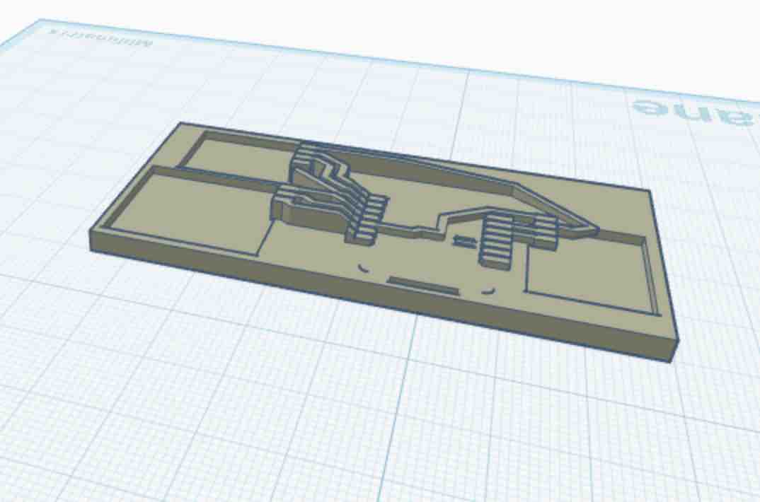
05 | This is the final design I printed on the 3D printer
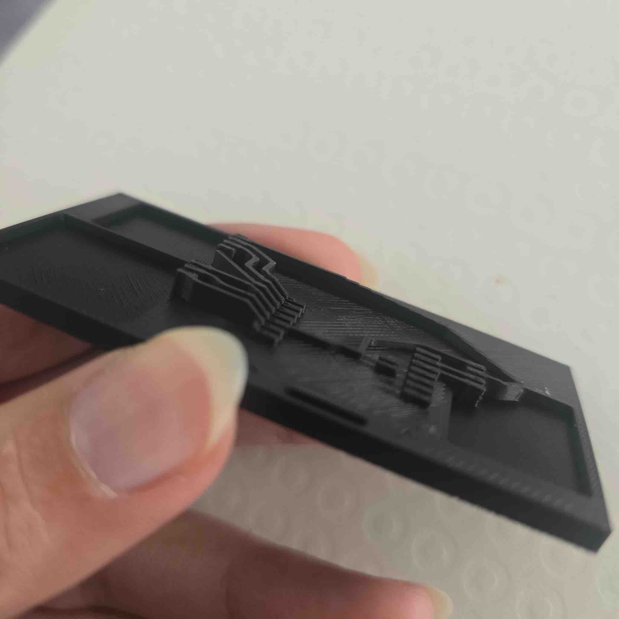
06 | This is how it looks — so cool! Now I will start adding the copper tape on top and cleaning the routes.
07 | I aligned the components here but haven't soldered them yet for testing.
- Feedback: I can think of endless shapes and 3D PCBs I want to try and make.
- Challenge: I keep feeling like I'm behind schedule because I'm trying everything except a copper PCB. I really feel overwhelmed at this stage and I'm not sure if I'll ever get a milled PCB!!! But this 3D-printed approach looks like a good alternative.
03: Finally, Copper PCB
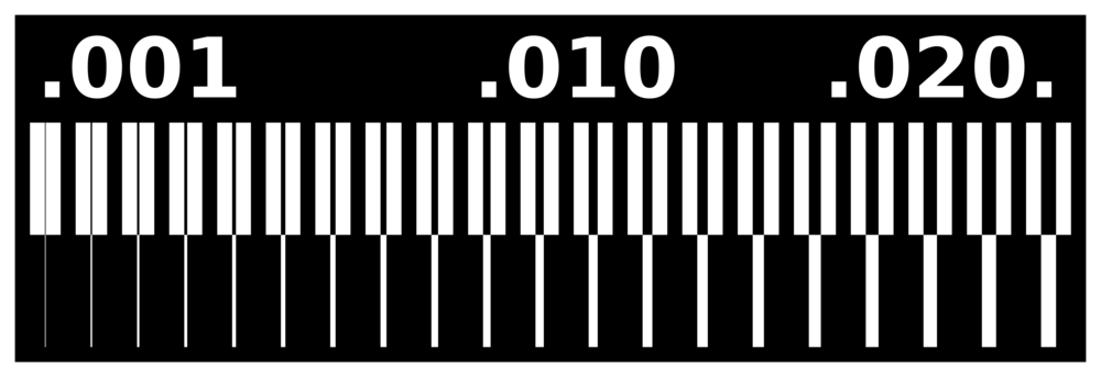
01 | The first thing I tried when I received the PCB stock and the end mills was to run a test cut with different routes. I tried to follow the instructions from the one and only Adrián Torres, but we couldn't execute that as we weren't using Mods — and I couldn't transform this PNG file into a G-code file to use on our CNC.
02 | I created a PCB test file in KiCad with tracks at different widths from 0.2 mm to 0.9 mm.

03 | I imported the file into FlatCAM and generated the G-code file for the CNC, with different depth settings from 1 mm down to 0.35 mm, using a 0.2 mm end mill and V-bits with tip angles from 30° to 15°.
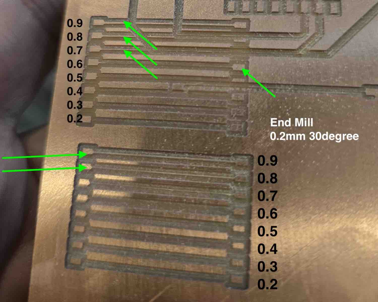
04 | I checked the routes' connectivity using a multimeter and found that the best setting for me was to design PCBs with routes 0.7 mm and above.
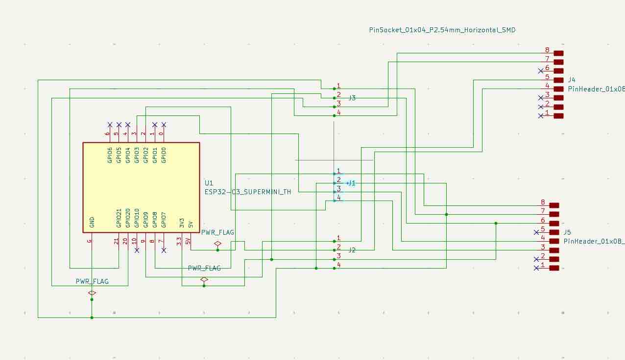
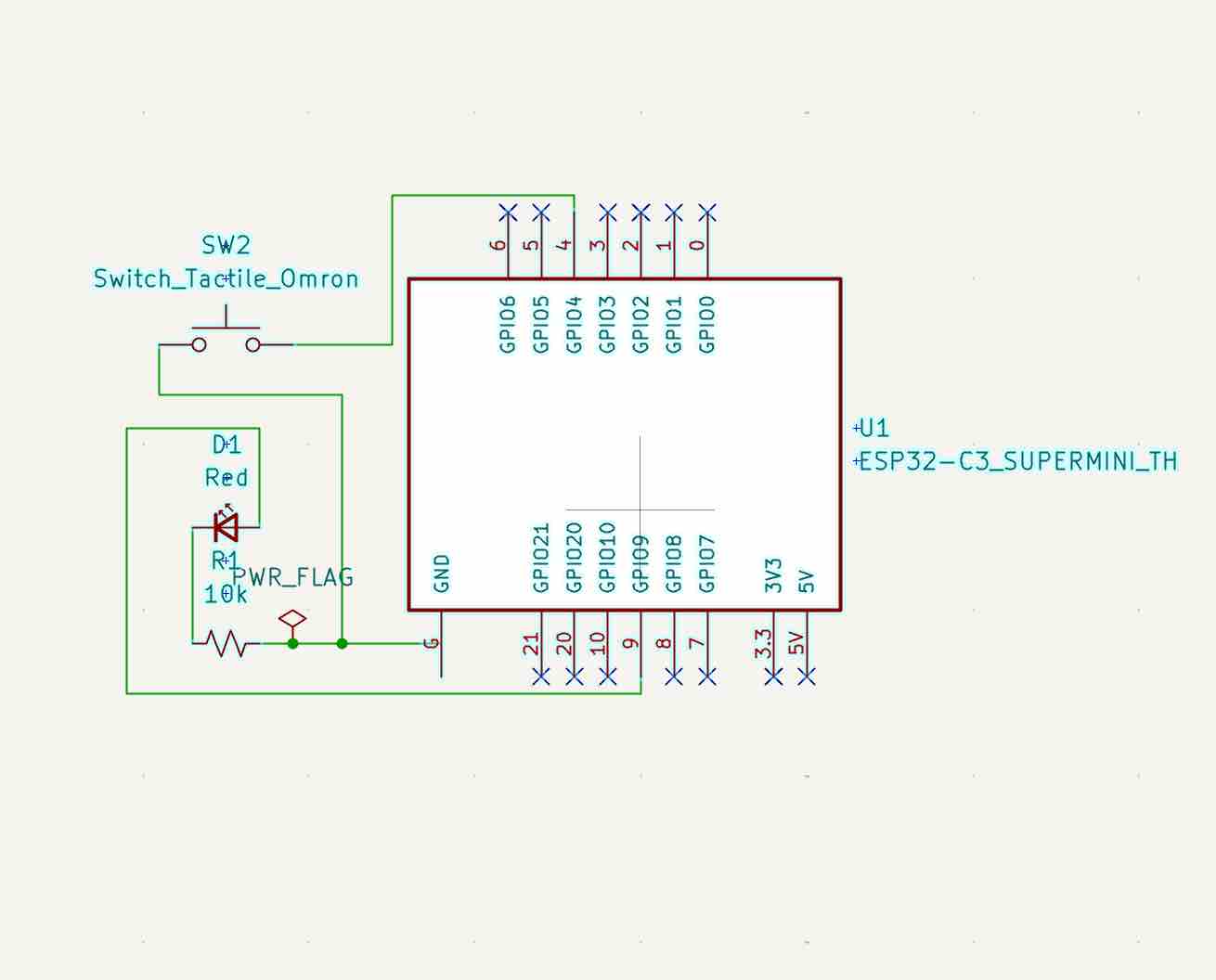
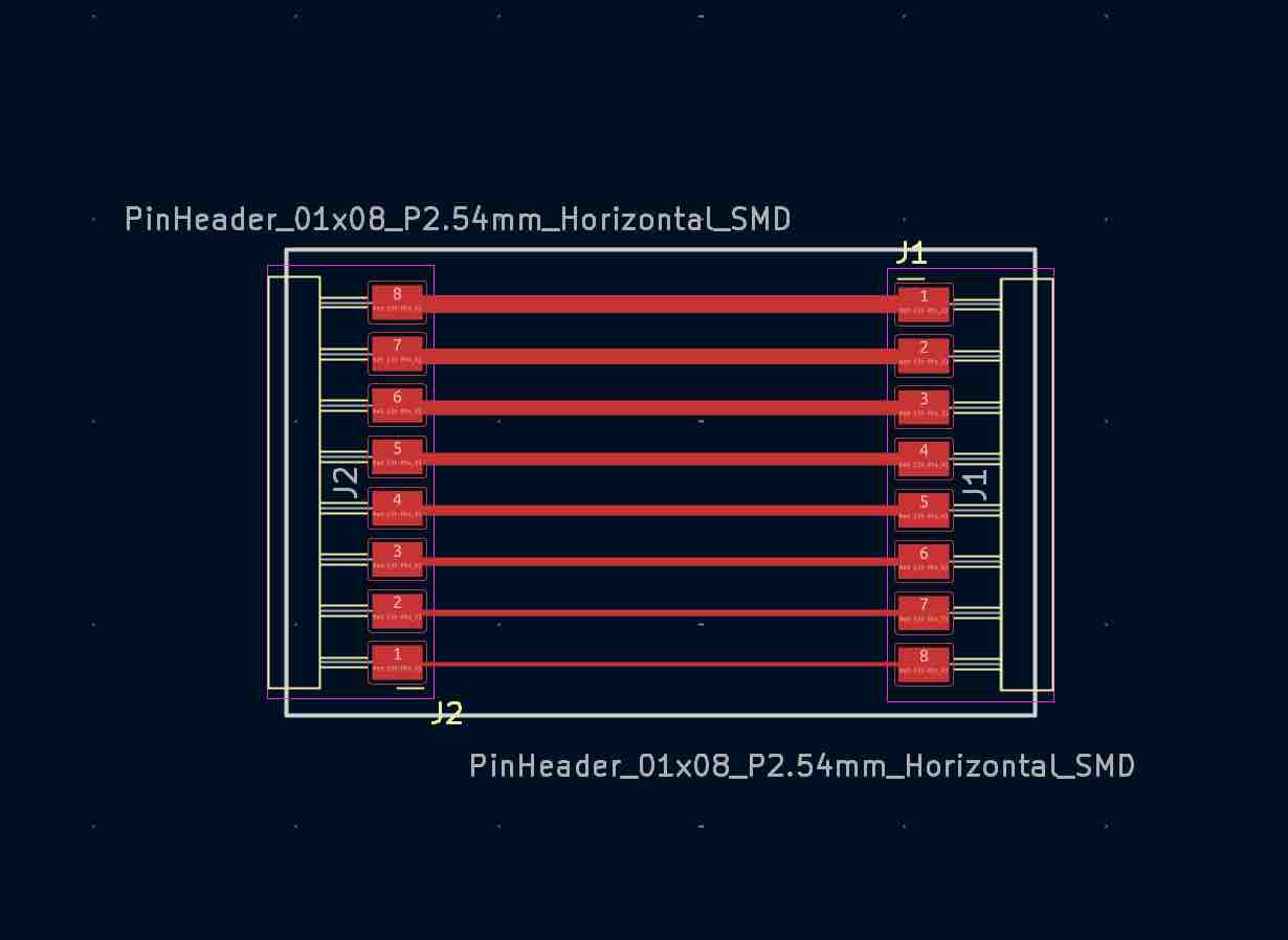
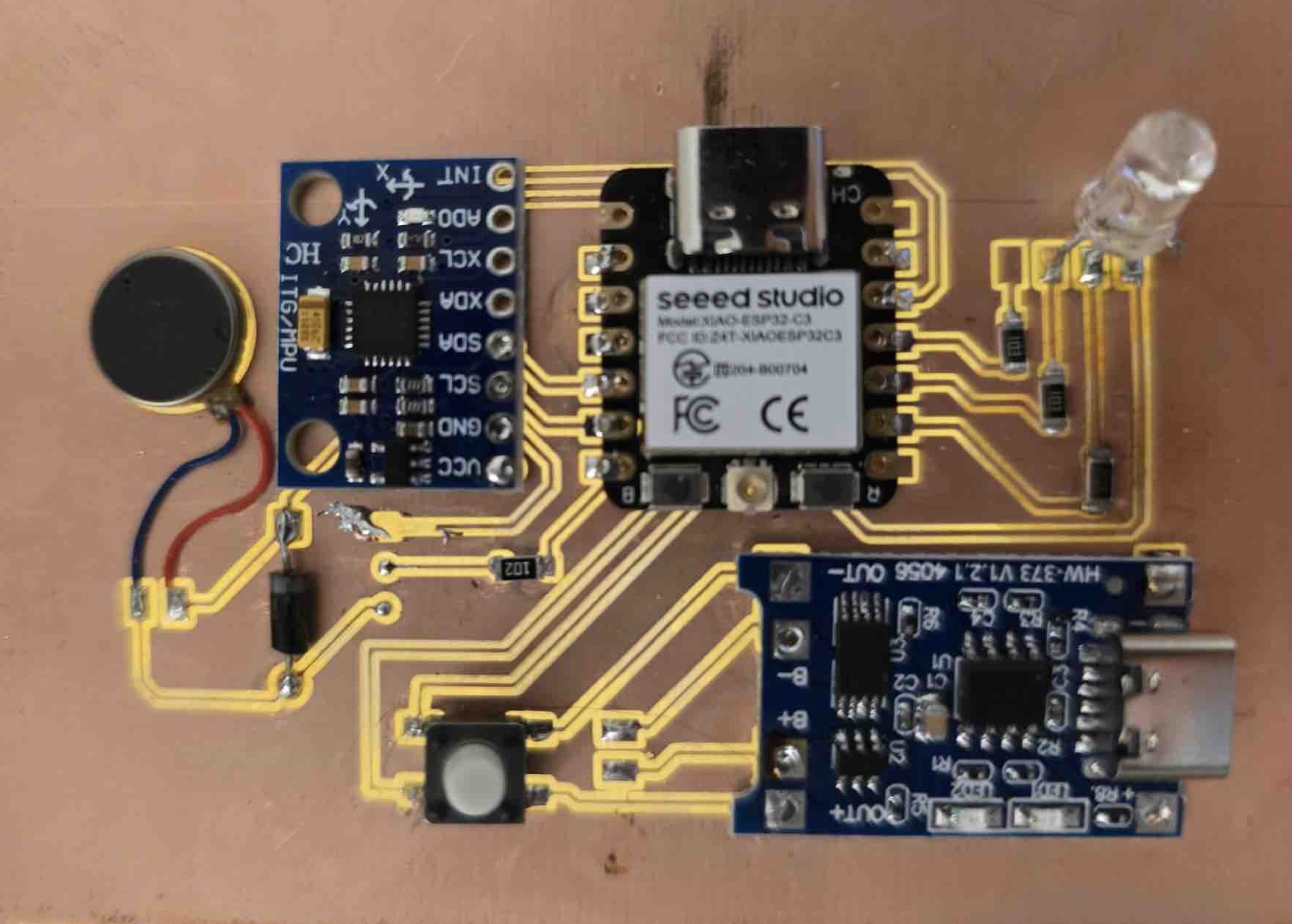
05 | Then I designed a universal PCB with 3 ports that can be used as either inputs or outputs. The design was made in KiCad — this is the schematic, and here is the link to the complete file.
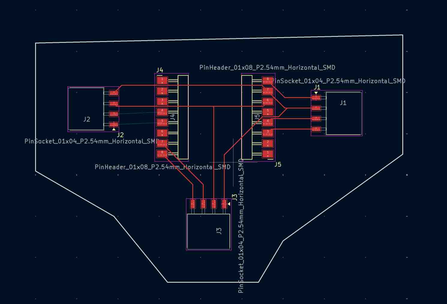
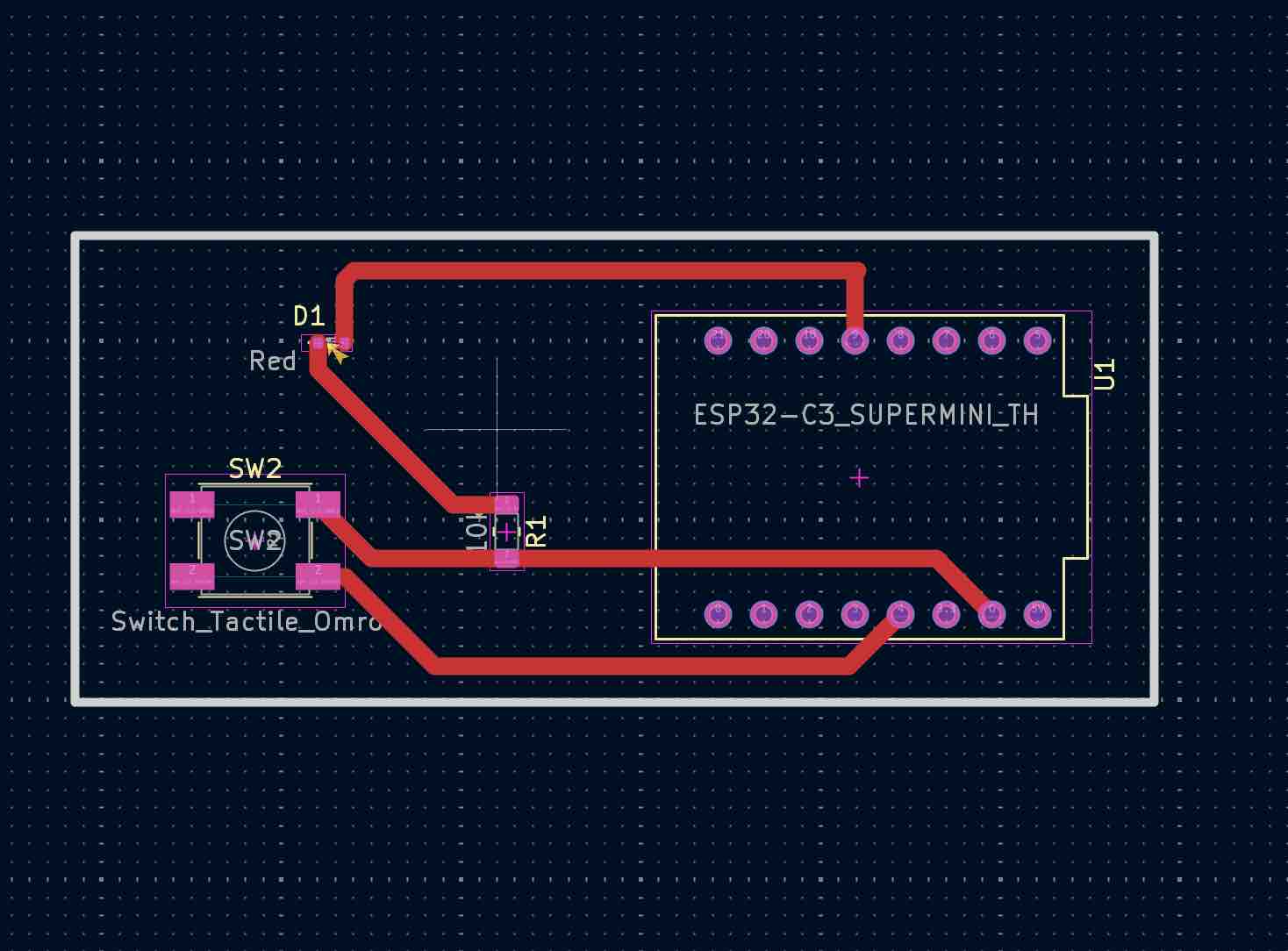
06 | In the PCB Editor I aligned all the ports to allow attaching different inputs and outputs, with a track width of 0.5 mm — and shaped the PCB like an airplane.
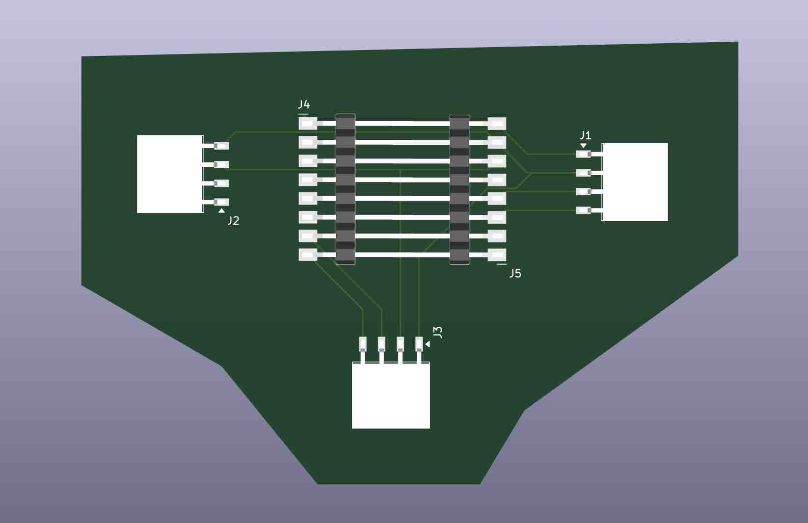
07 | This is the 3D design — it shows that I can even swap the microcontroller and retest things. It's also very useful because I don't have access to a large quantity of PCBs.
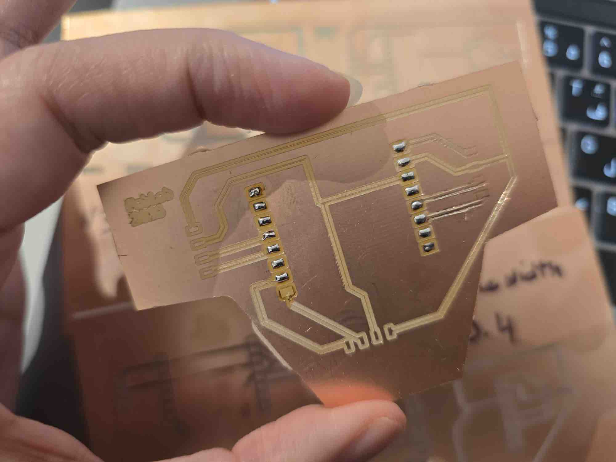
08 | And this is how it looks. I also tried soldering and testing the routes with a multimeter.
- Feedback: Huge relief to be able to complete my upcoming assignments — and a bigger chance to be able to graduate in the first cycle.
- Challenge: We ordered PCB boards from two different sources, and the settings for each board were different. Running the test file helped a lot in defining the settings for each brand.
04: Microcontroller on PCB
I received the PCB boards in Week 14 of the Fab Academy cycle — considered very late. I tried to make a universal PCB but I was running out of time, so after milling the test PCB in point 03, I moved on to milling the PCB for my final project. In Weeks 8, 9, 10, and 11, I documented the workflow I followed for my final project PCB.
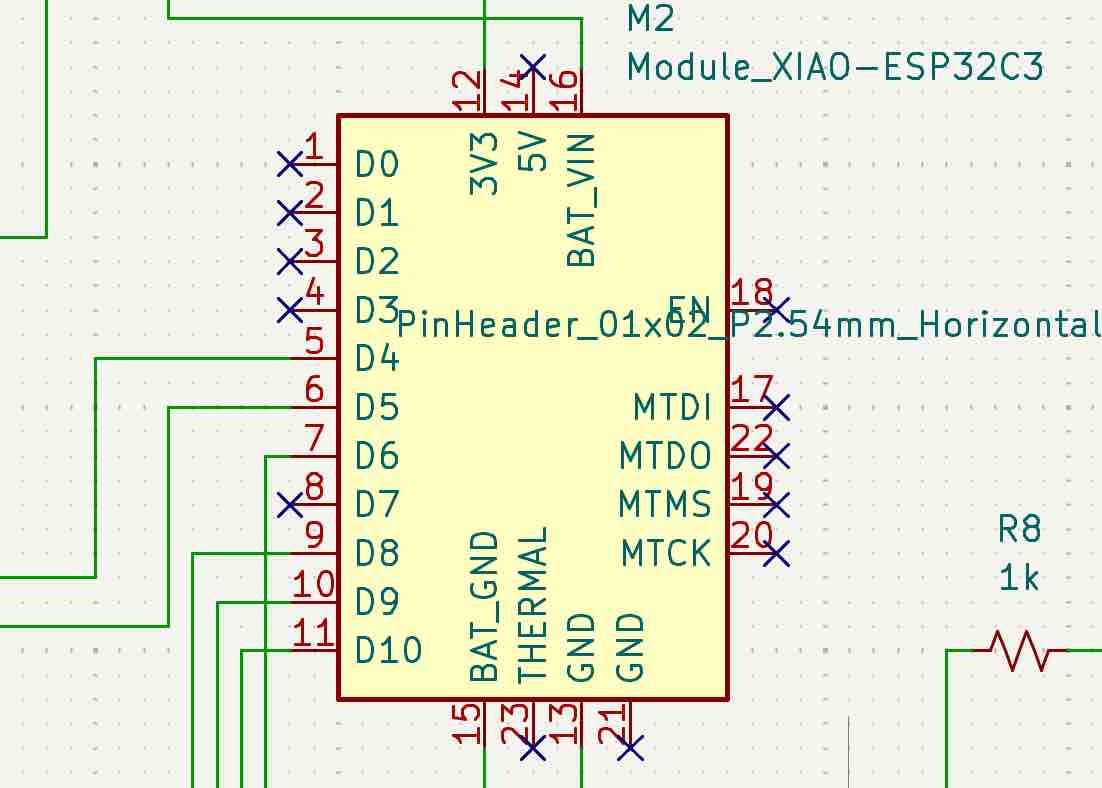
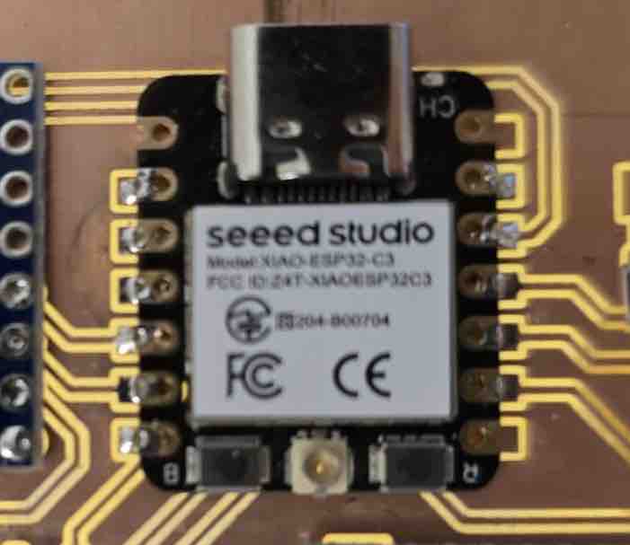
01 | This is the schematic design for the ESP32-C3 XIAO.
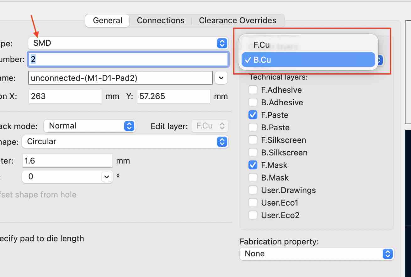
02 | In the PCB design, I moved some of the pins and pads to the back of the circuit (B.Cu layer).

03 | This is mainly because I had to draw routes running under the microcontroller, branching out to different inputs and outputs — to avoid short circuits and Design Rules Check (DRC) errors. I kept the battery connections on the same side so they stay connected to the charging module outputs.
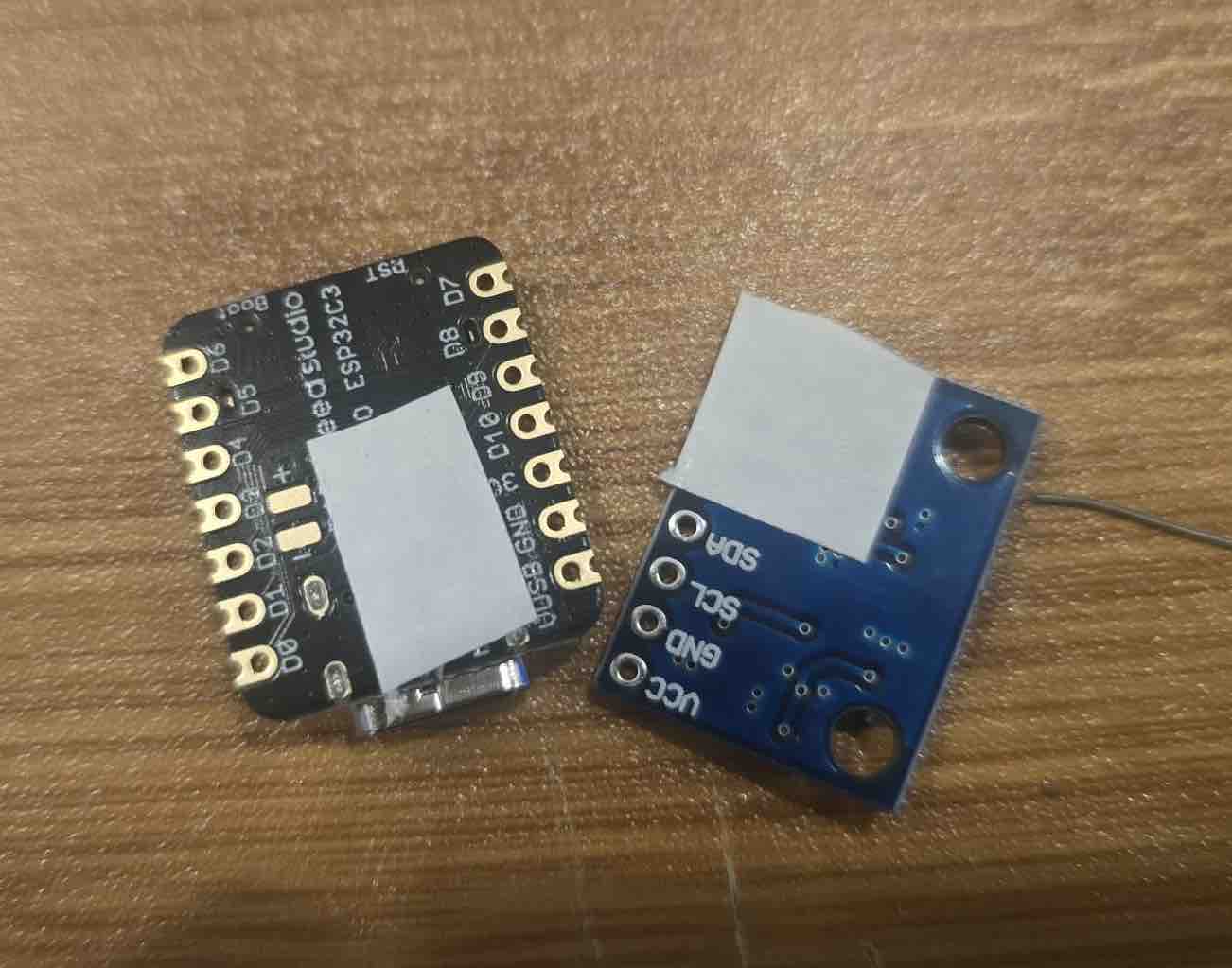
04 | In practice, I added tape to isolate the unneeded conductive pins from the PCB routes branching out to the sensors.
05 | This is how it looked at the end.
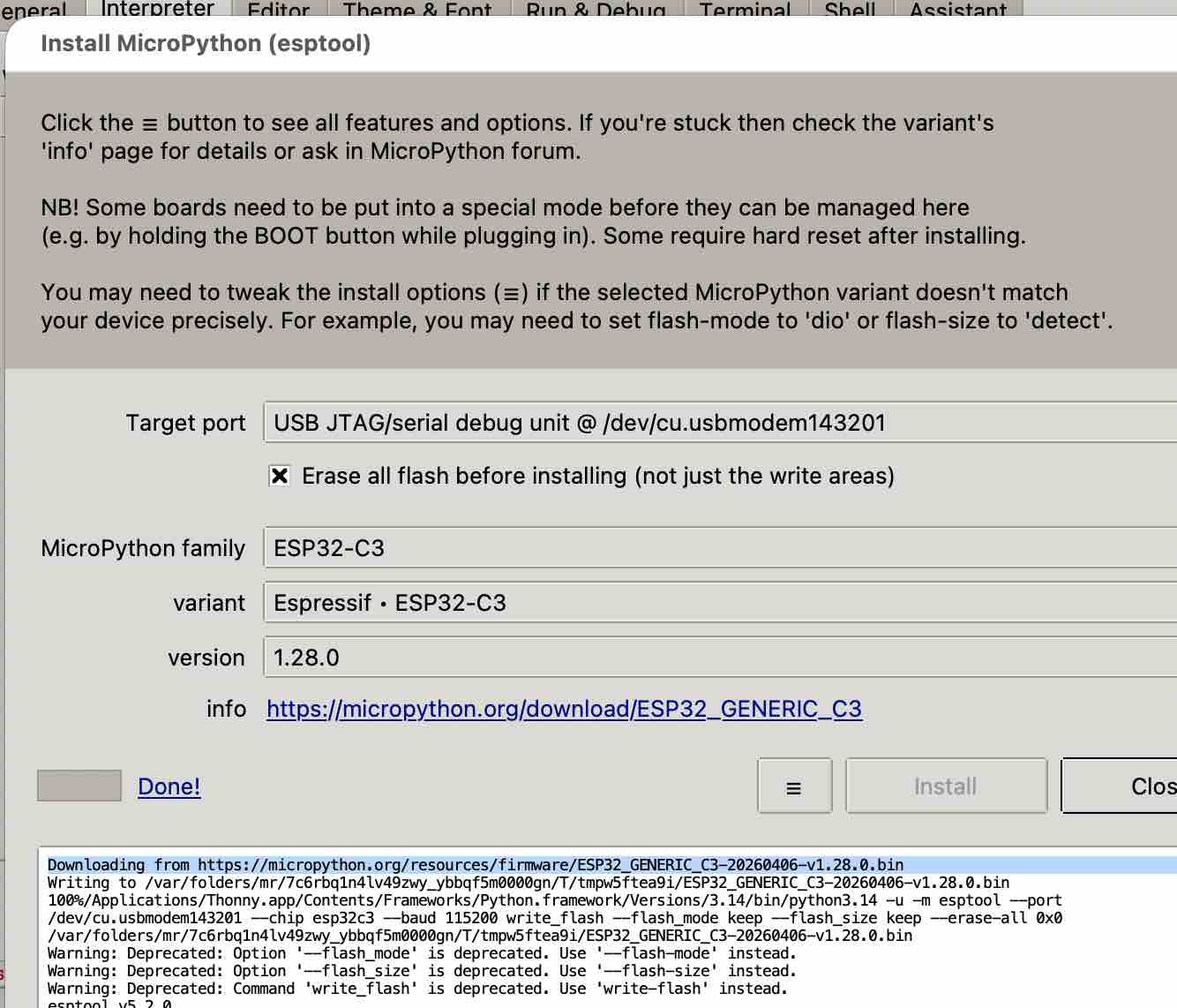
06 | After flashing the MicroPython firmware to the microcontroller using Thonny, I started with the Bluetooth connectivity to make sure the microcontroller was up and running.
07 | Next I started working on the final project PCB. The full workflow is documented here.
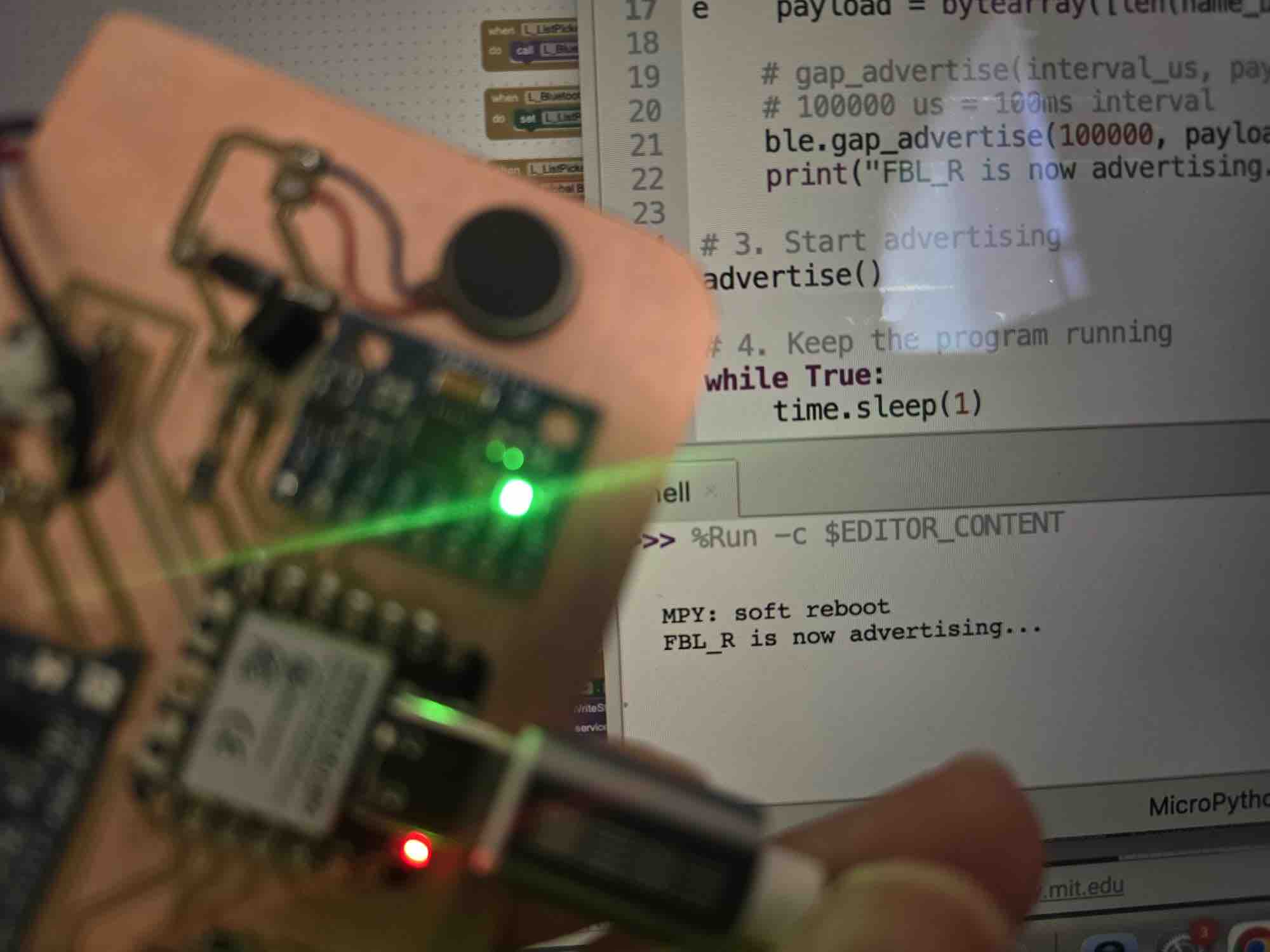
08 | The first test for the microcontroller was advertising its name so it could be discovered over Bluetooth by other devices.
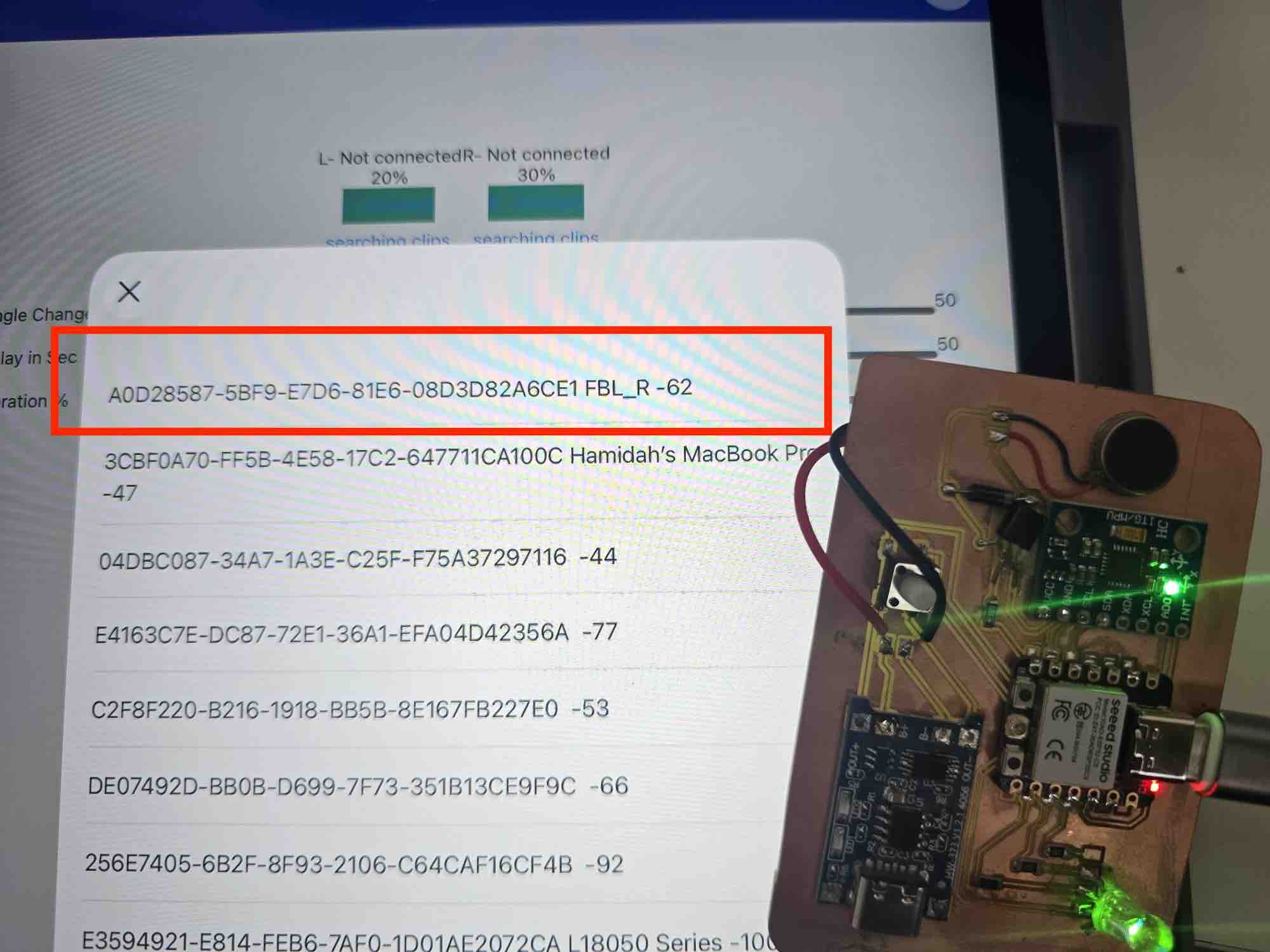
08 | The first test for the microcontroller was advertising its name so it could be discovered over Bluetooth by other devices.
- Feedback: At this point I spent 3 days finalizing the PCB that included the microcontroller, 1 input, 2 outputs, and a charging module. I had to redo the schematic and PCB design multiple times in the software, but I wasn't able to test the result until Week 14. It could have been easier if I'd had the parts on time — but I was able to get it done.
- Challenge: Digital design without being able to fabricate is not easy. Having to keep using alternatives forced me to try other skills I might not have wanted to attempt under time constraints. It was an exciting learning experience, but a really stressful one.