The process
My experience in this area is very limited, and the mini-course on electronics presented by Monther from Vujadé helped me organize my thoughts and figure out how to start.
Group assignment
As a remote student, I joined the VujaDé Lab session online from Kuwait while the team in Saudi Arabia ran the bench. The group assignment for this week is to use the test equipment in our lab to observe the operation of an embedded microcontroller — we covered the digital multimeter and the digital oscilloscope on an Arduino test board.
01: Using test equipment
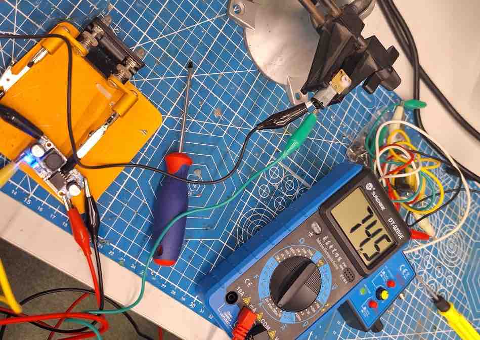
01 | Digital multimeter — we used it to verify the basics of the circuit.
- Continuity: tested the connections between different jumper wires and the power supply to confirm there were no breaks.
- Voltage: measured the 5 V and 3.3 V output pins of the Arduino to confirm that the power supply was stable and accurate.
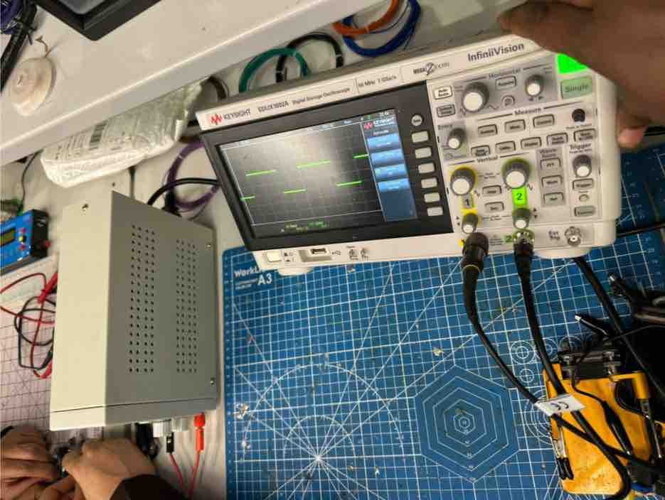
02 | Digital oscilloscope — to observe the "invisible" behaviour of electricity. We wanted to see how the Arduino actually controls power using Pulse Width Modulation (PWM).
- Setup: connected the oscilloscope probe to the PWM pin (Pin 9) running the Arduino "Fade" example sketch.
- Observation: unlike a multimeter — which shows a steady average voltage — the oscilloscope revealed a square wave: the pin is rapidly switching between 0 V and 5 V, and the duty cycle determines the perceived brightness.
analogWrite(): we discussed how this function doesn't actually output an analog voltage. It outputs a fast digital signal (≈ 490 Hz on most pins, 980 Hz on pins 5 and 6 of the Uno). The "analog" effect is just our eyes / loads averaging the high-frequency switching.
- Feedback: As someone with no electrical-engineering background, this information was very valuable — especially because in my final project I need to control the strength of the vibration motor and the LED brightness, which is exactly what PWM (driven by
analogWrite()or its MicroPython equivalent) lets me do. Going from "the LED looks dimmer" to "the duty cycle is 50%" is a big mental shift. - Challenge: Looking forward to receiving our shipment and devices on time to use them while we develop the project. As a remote student living in Kuwait while the lab is in Saudi Arabia, having the equipment locally is what would let me do bench-checks myself instead of relying on the global session.
Individual assignment:
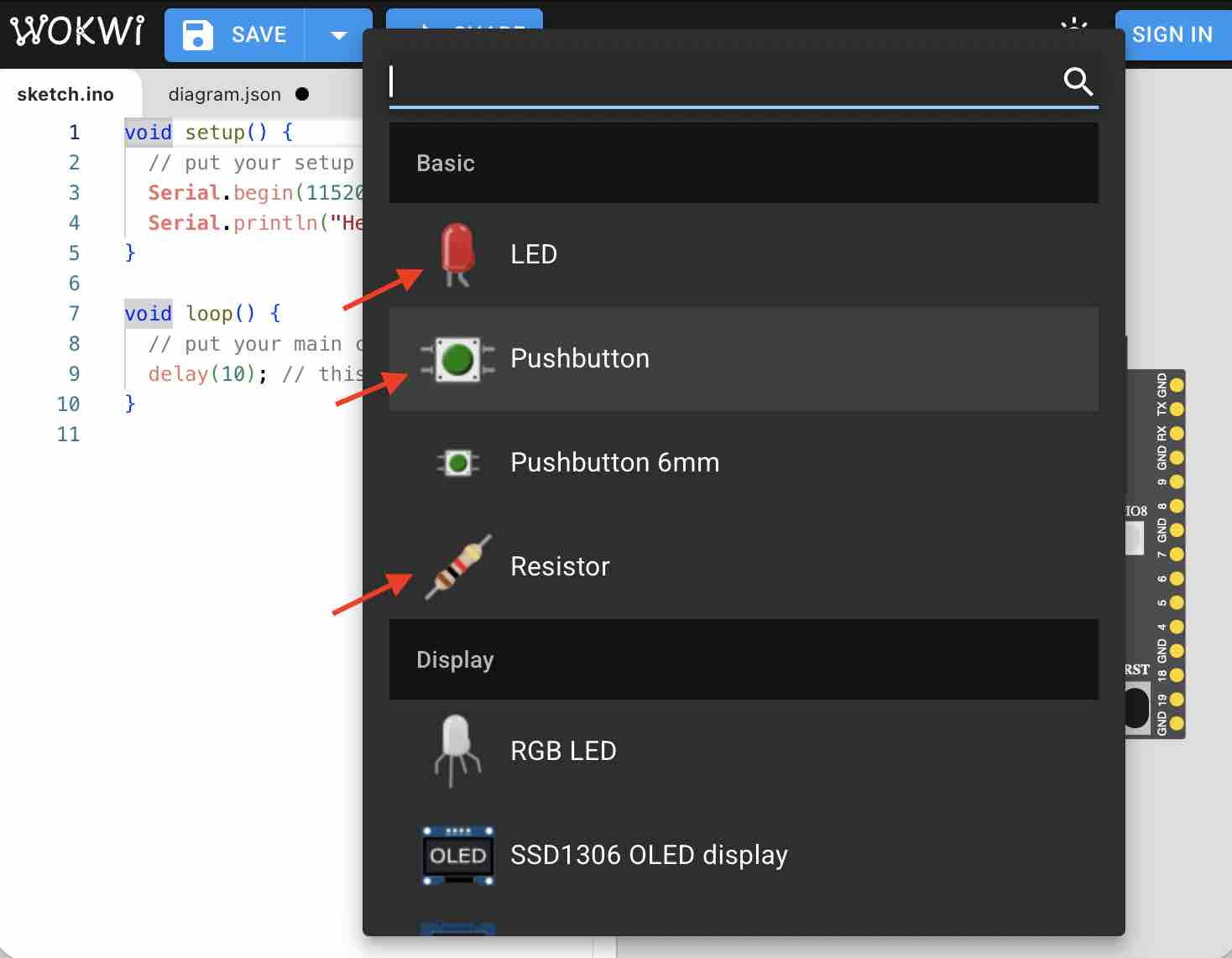
01: Simulate a circuit (Wokwi)
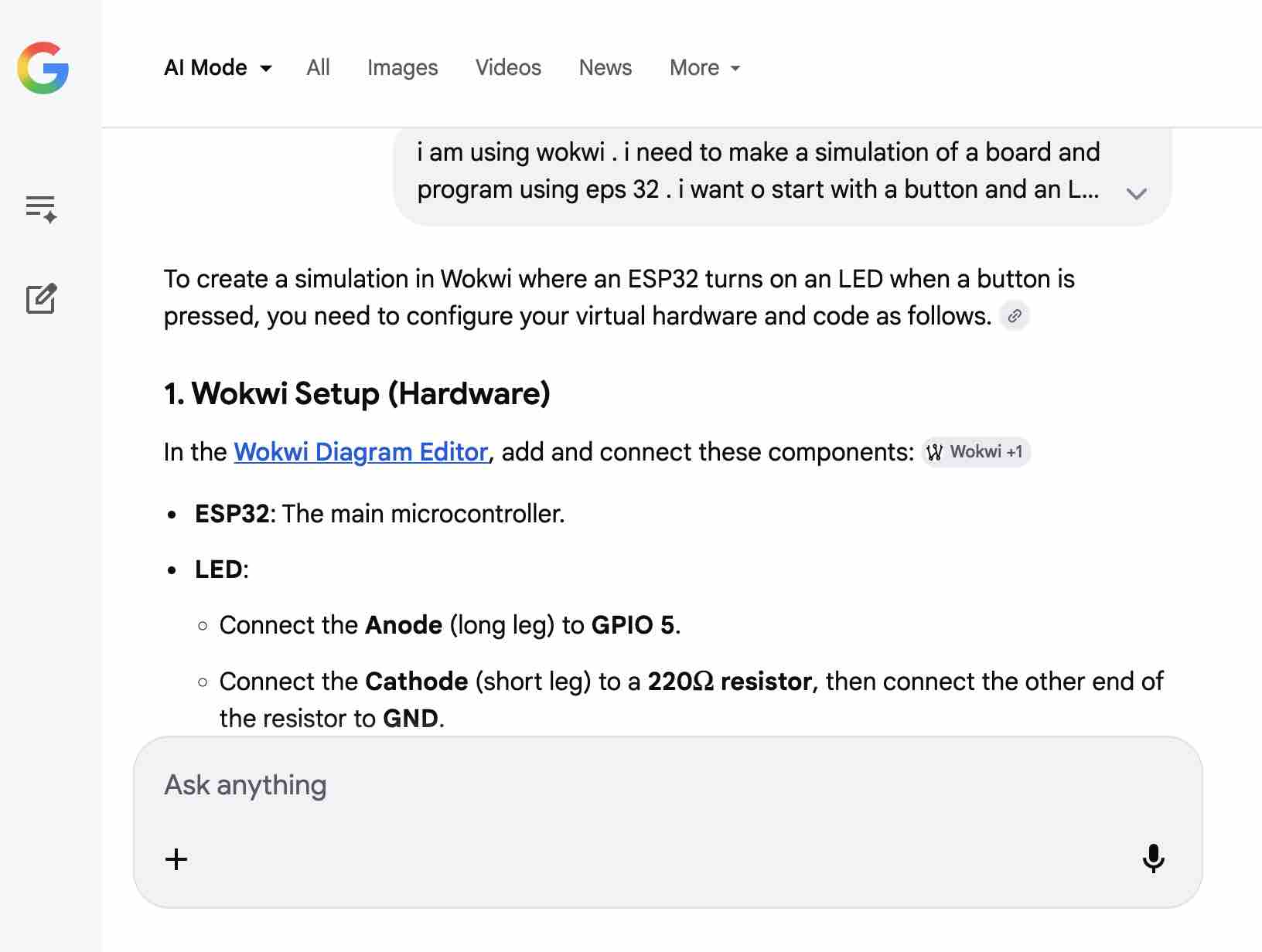
00 | I started this task by asking Google AI Gemini to provide me with steps to use Wokwi to design and simulate a simple circuit
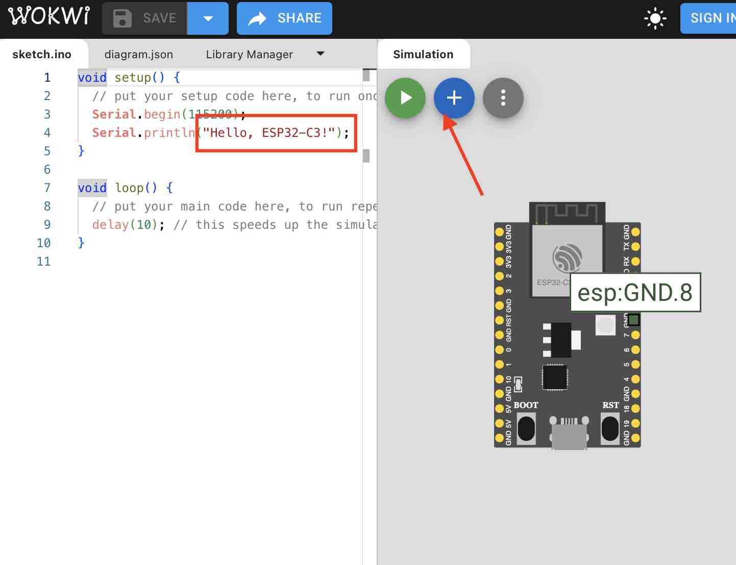
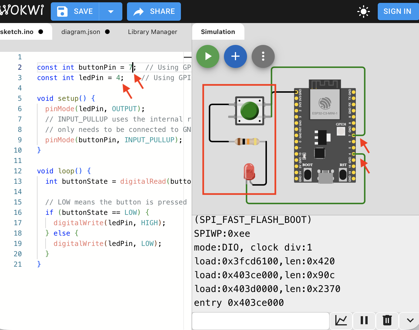
01 | I selected to work with ESP32-C3, then I added new parts for the list
02 | I selected a red LED, a button, and a 10K resistance for the button
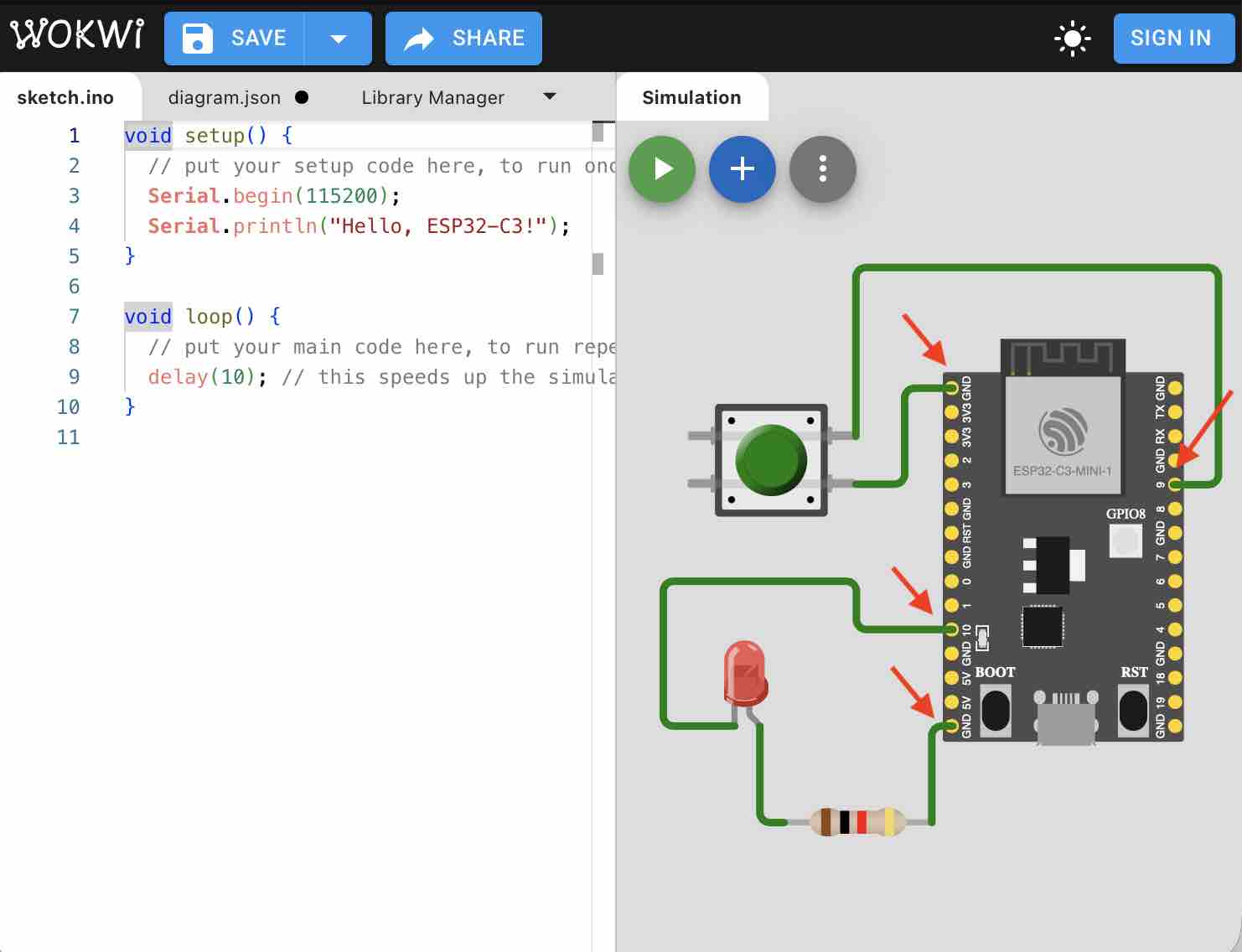
03 | I connected the parts as shown in the drawing. The LED anode is connected to the resistor and then to ground on the microcontroller. The LED cathode goes to pin 10 on the microcontroller. I also connected one leg of the button to the ground of the microcontroller, and the other leg to pin 9
04 | I copied the code from Gemini AI, which first defines each pin to a variable name, then uses an if-condition to define the behavior of the circuit
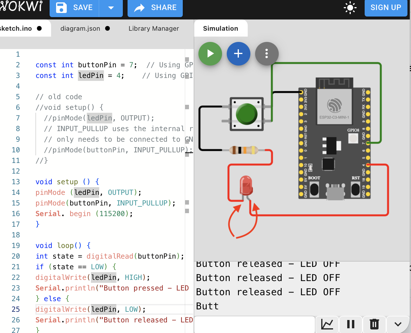
05 | Deleted the default code in the simulation and ran the simulation, but it did not work.
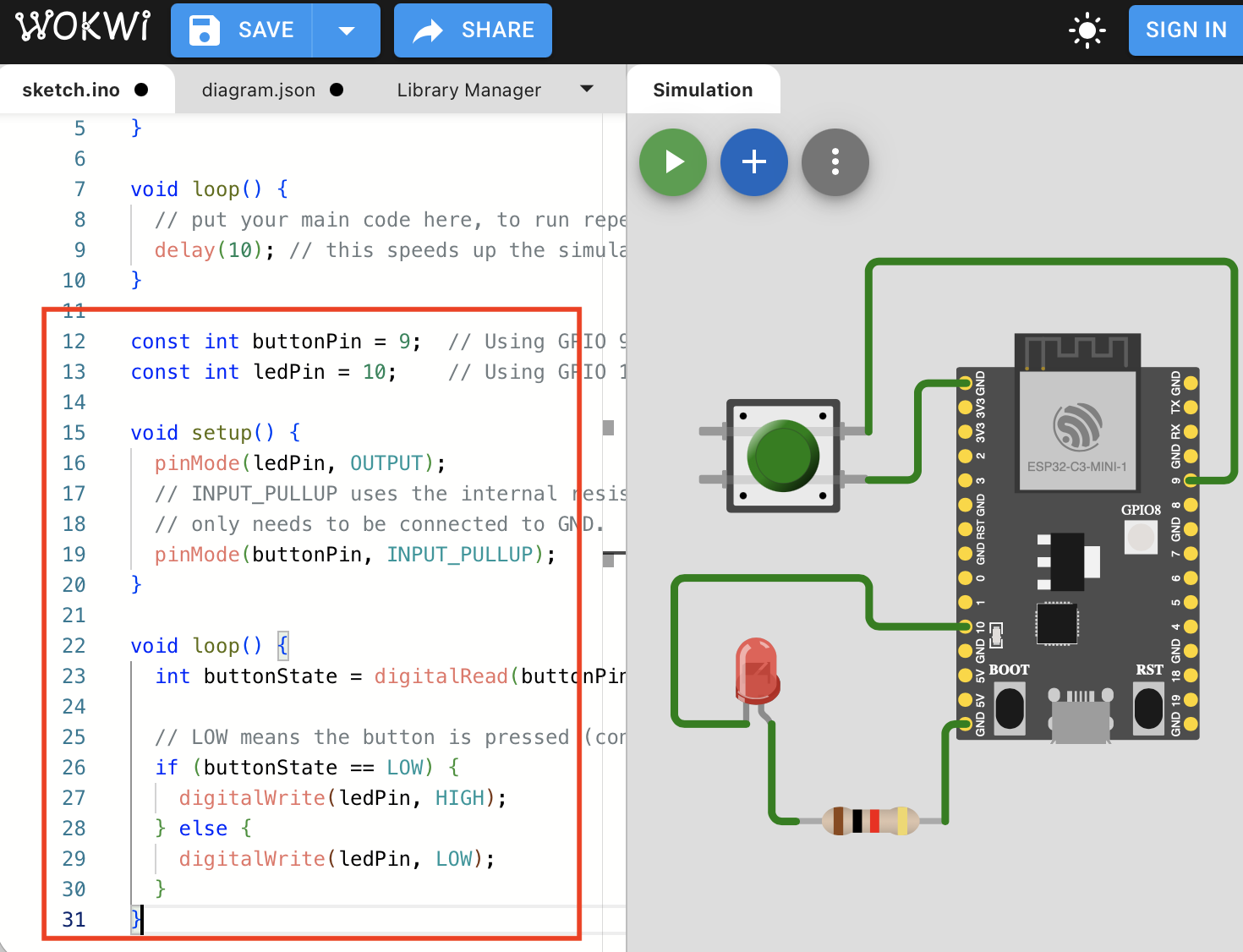
06 | I followed the documentation by Musaed AlKout and changed my circuit to connect the LED to the button instead of to ground
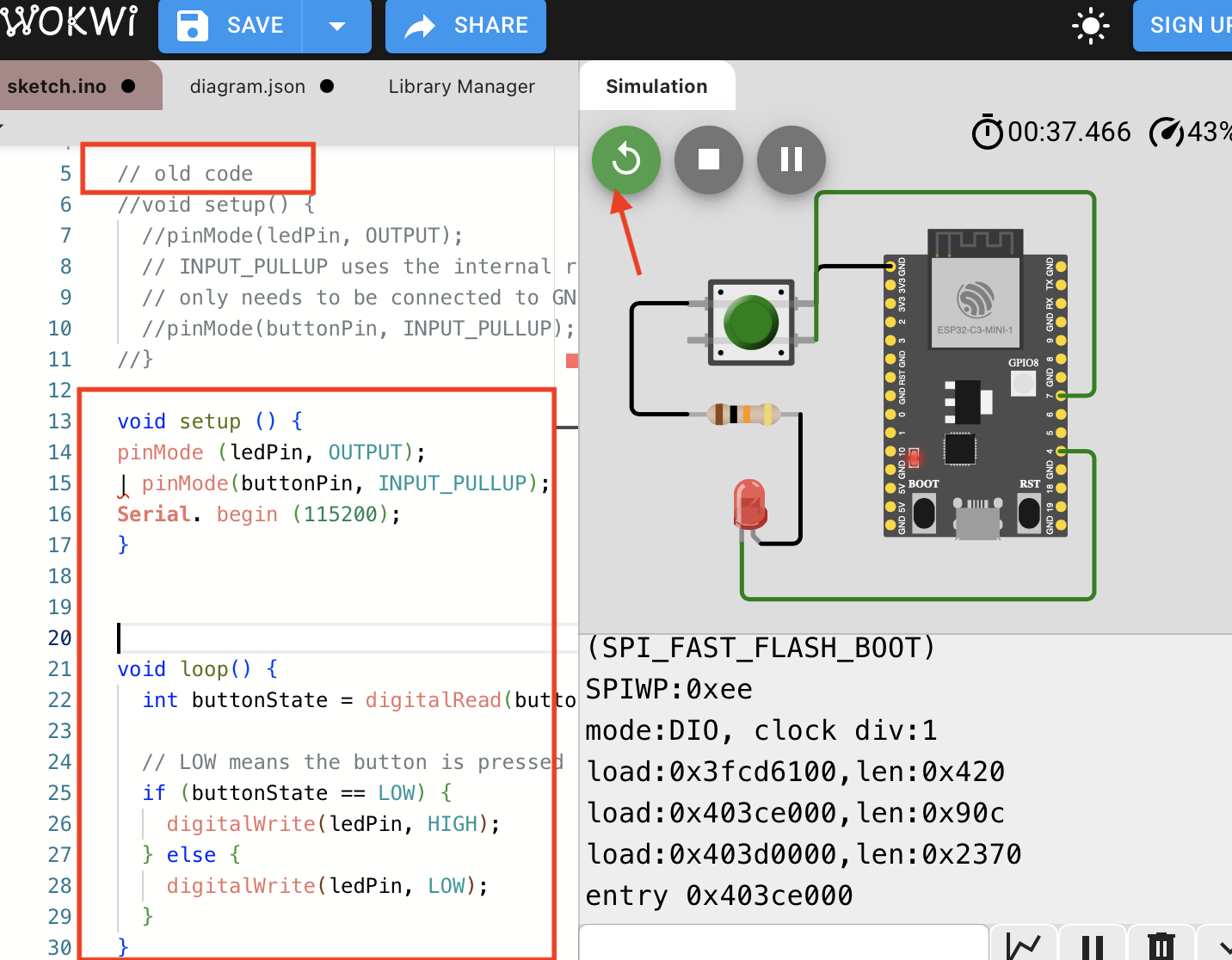
07 | After running the circuit, the LED did not turn on. Then I changed the code and ran the simulation.
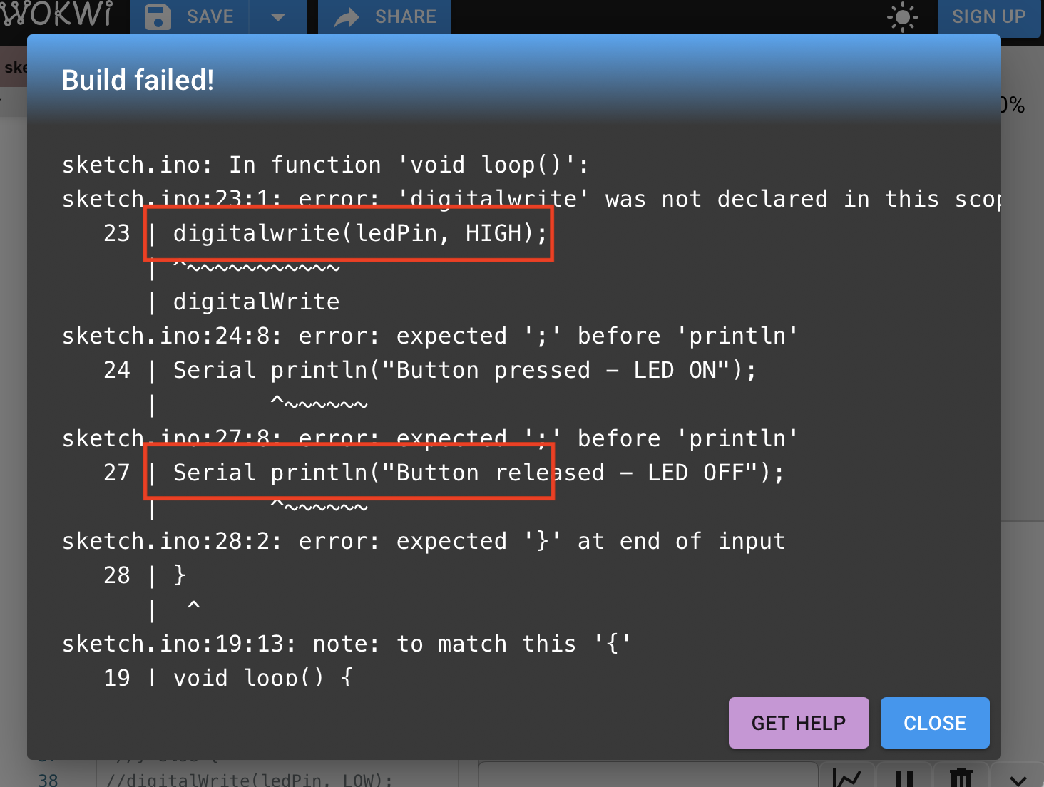
08 | There was an error in the syntax; I fixed the code
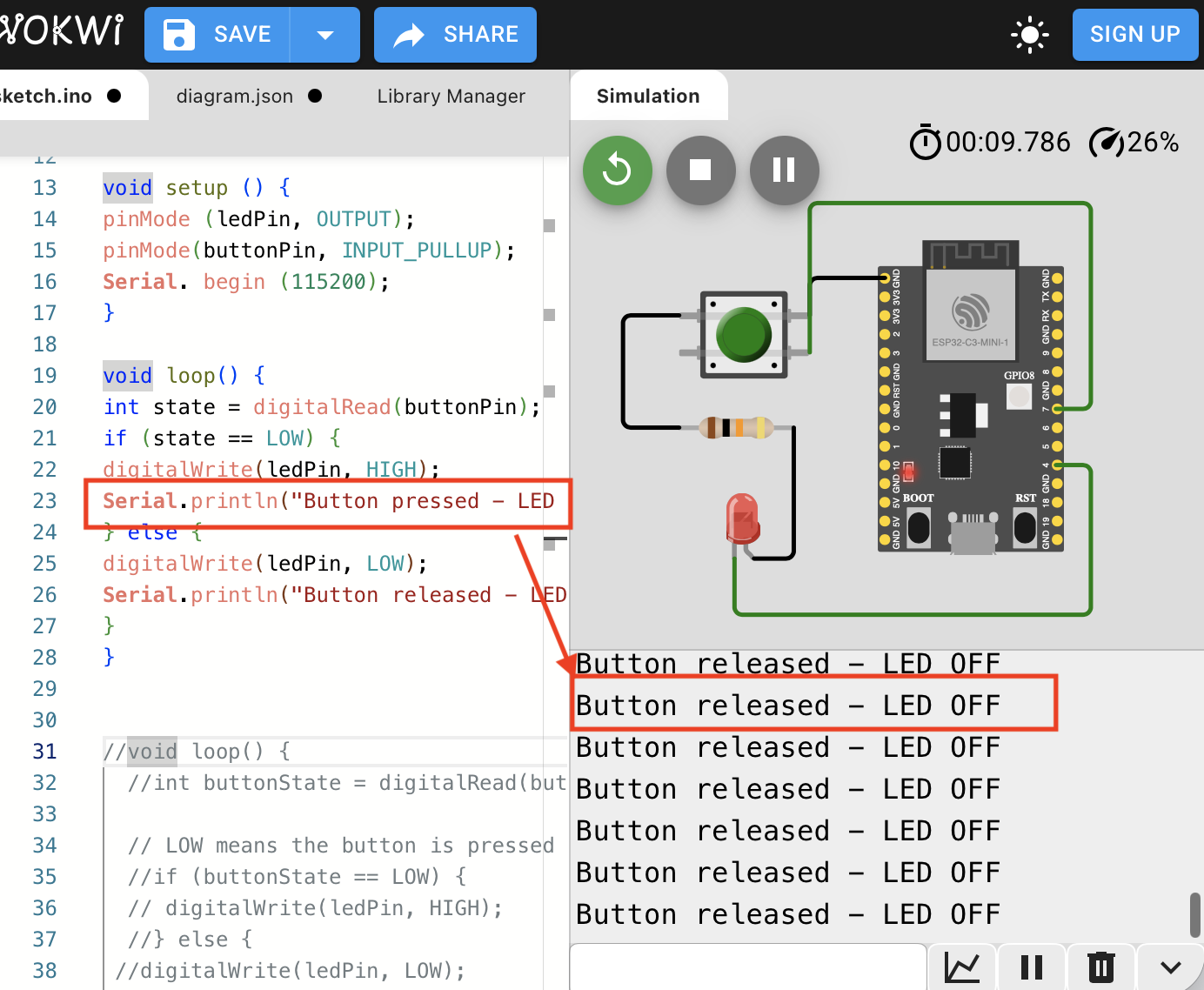
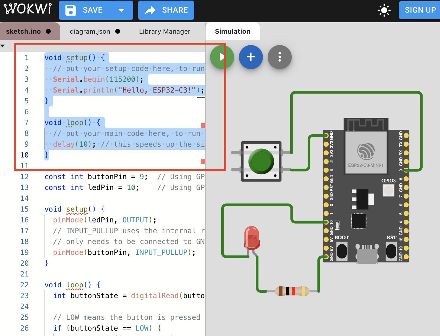
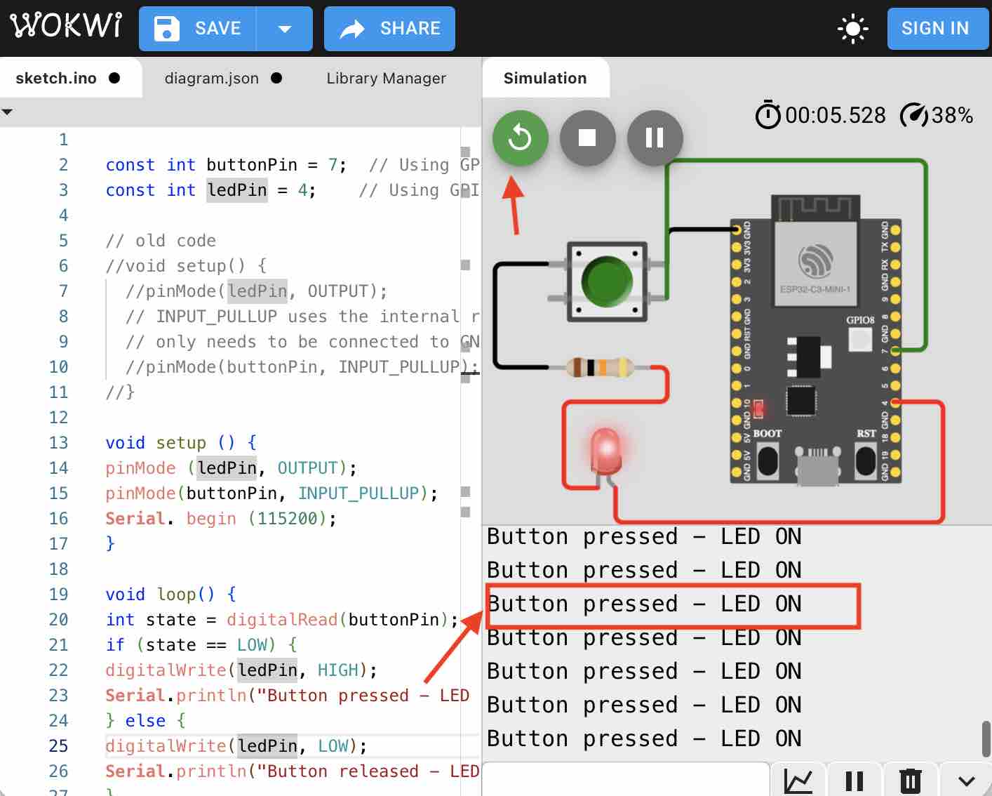
09 | When running the new code, the button was working, as the message "LED OFF/LED ON" was printed in the simulation — but the LED was not on yet
10 | I checked the connection, and after searching I found that I had misunderstood the LED legs. The short leg (cathode) is straight and the long leg (anode) is curved, even though it looked shorter. I switched the connections
11 | I ran the simulation and it worked — the statement "LED ON" is printed when the button is pressed and the LED turns red.
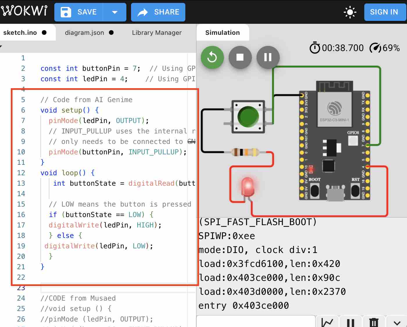
12 | Then I checked the first code generated by AI Gemini and it worked
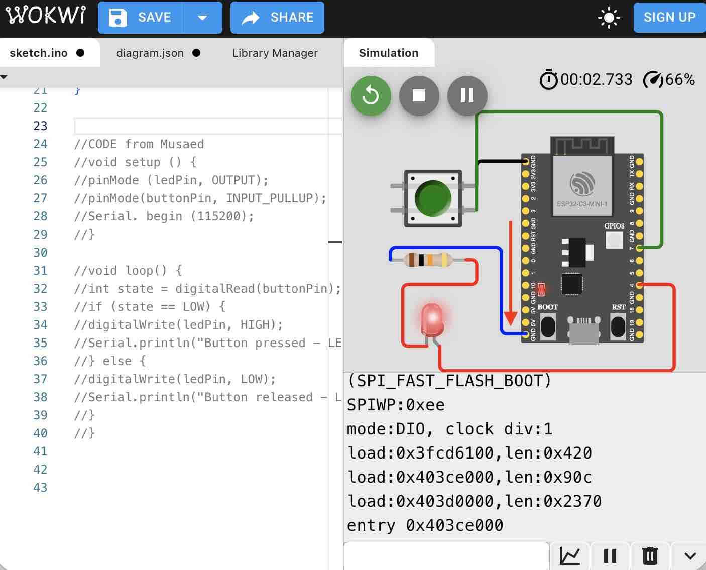
13 | Then I tried the connection as I made it the first time — disconnecting the LED from the button and connecting it directly to the ESP32 — ran the simulation, and it worked.
- Feedback: Understanding the graphics is very important, as well as making sure the code syntax is correctly written or pasted
- Challenge: Debugging is not easy when building circuits. Including the print command for the button component was very useful
02: EDA tool to design PCB (KiCAD)
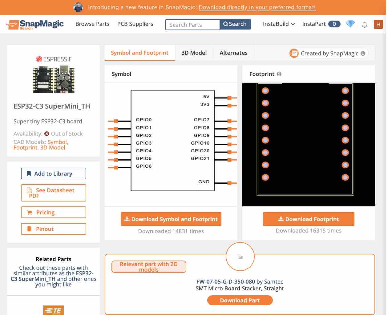
01 | I am using the ESP32-C3 SuperMini for my final project (continuing from Week 04 — Embedded Programming), so I had to get the footprint from SnapEDA
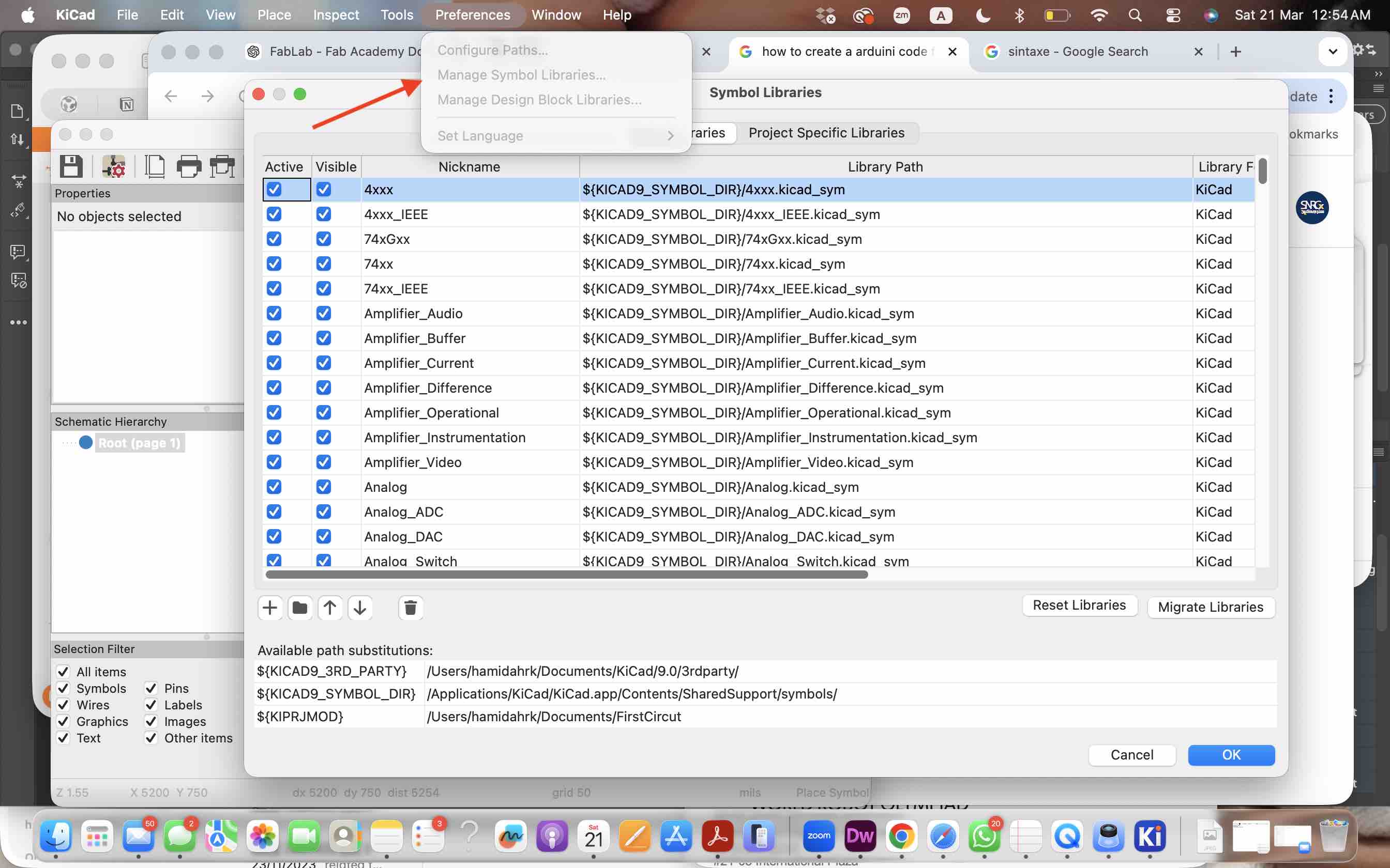
02 | I imported the files to the library of KiCAD
02 | I imported the files to the library of KiCAD
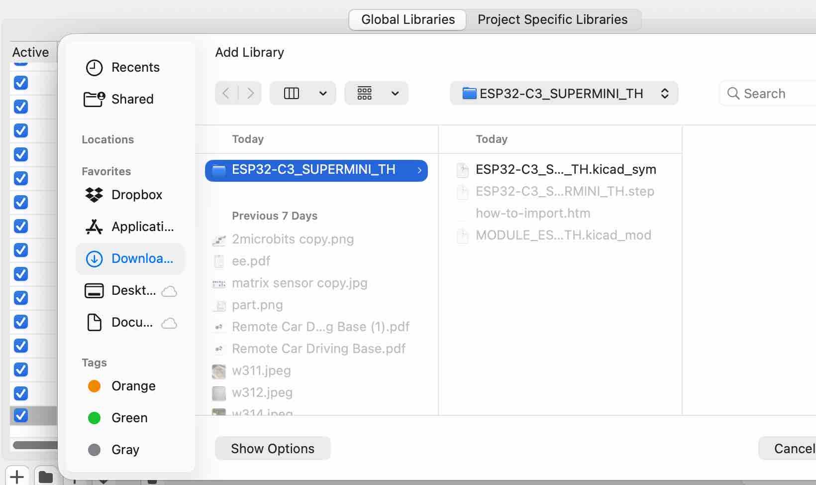
03 | Selecting the file be imported
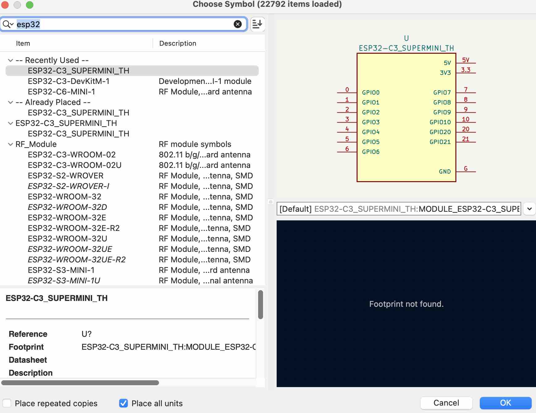
04 | I added the microcontroller, an LED, a resistor, and a button from the library
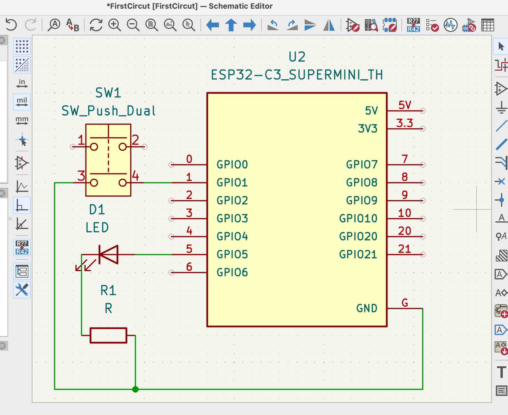
05 | I aligned them and connected them to create my PCB
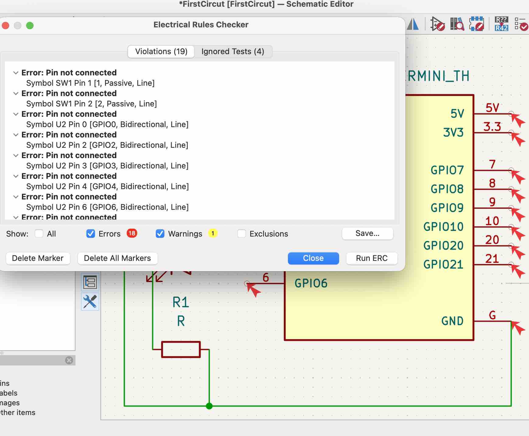
06 | I ran the Electrical Rules Checker to find the errors
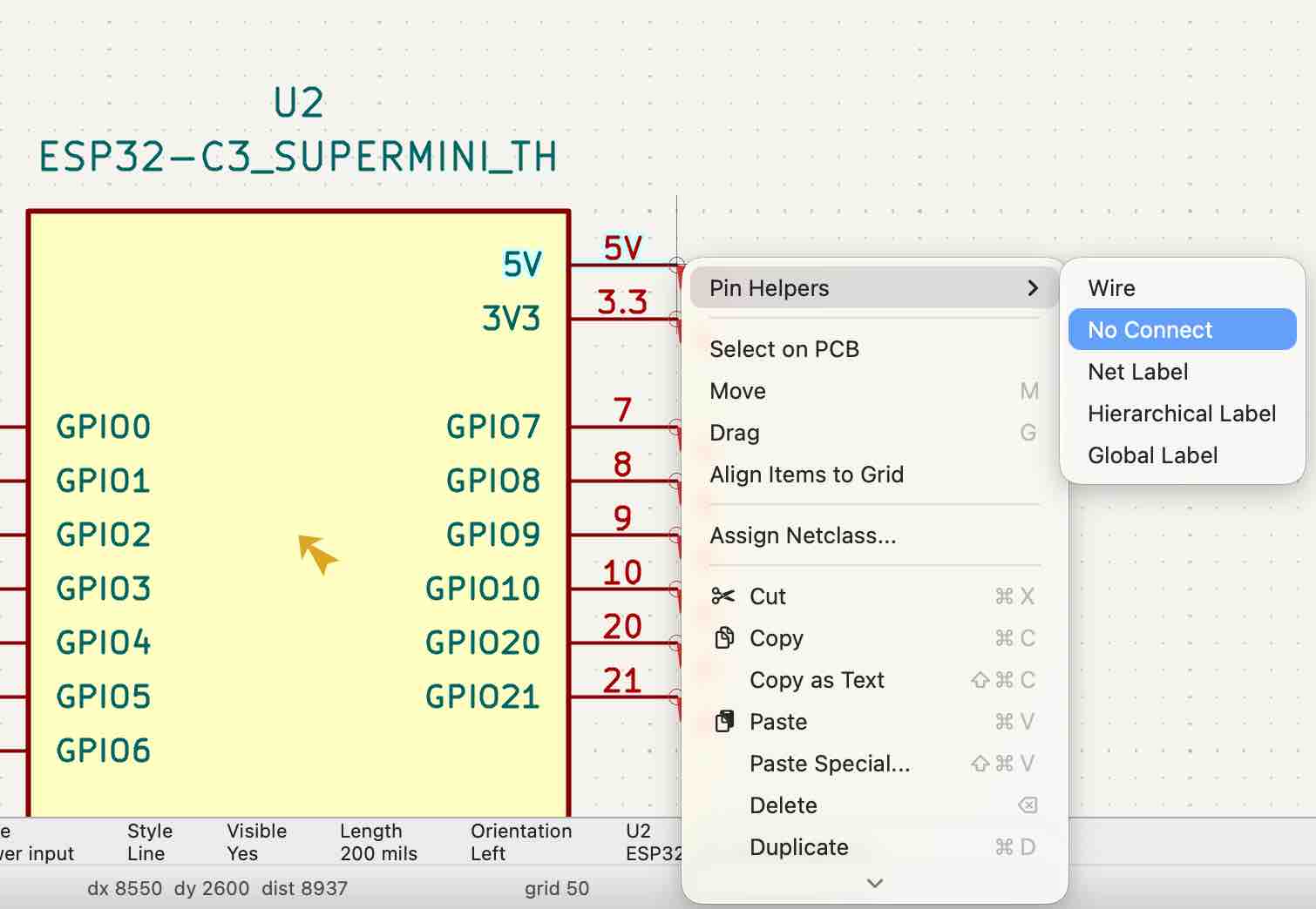
07 | Then I started to fix the errors, first by closing the pins that are not connected to anything
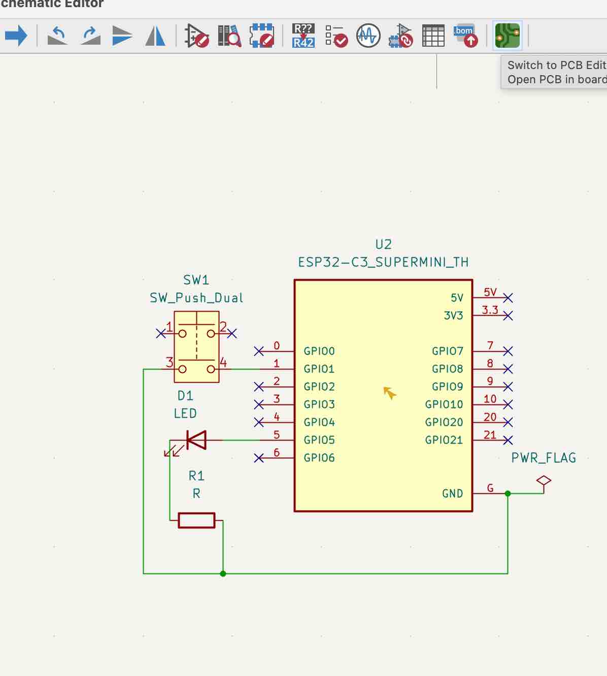
08 | Then I added a power-flag net to the ground connection and all the errors were fixed
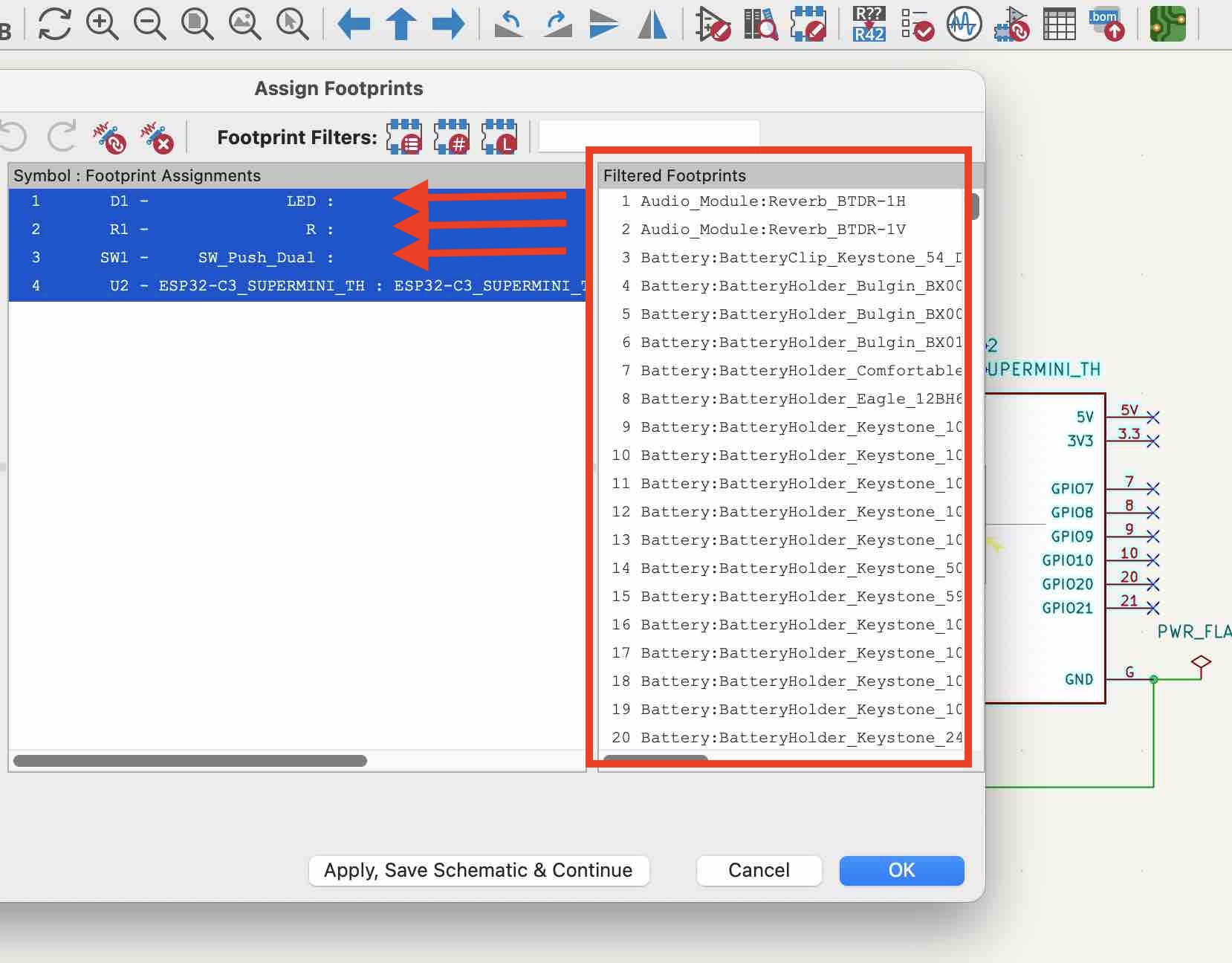
09 | Then I assigned the footprints to each part from the list
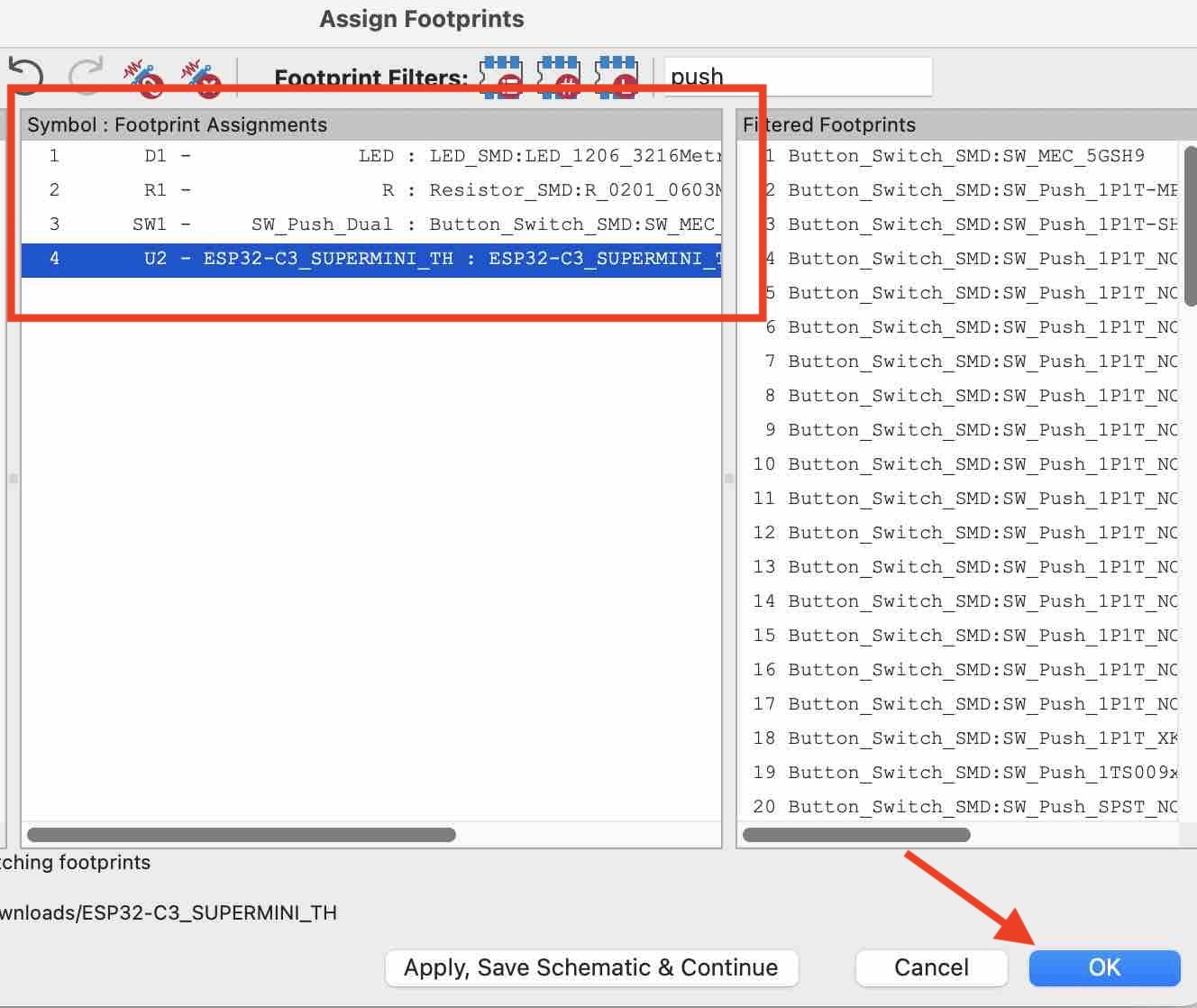
10 | Footprints assigned — now ready to switch to the PCB Editor.
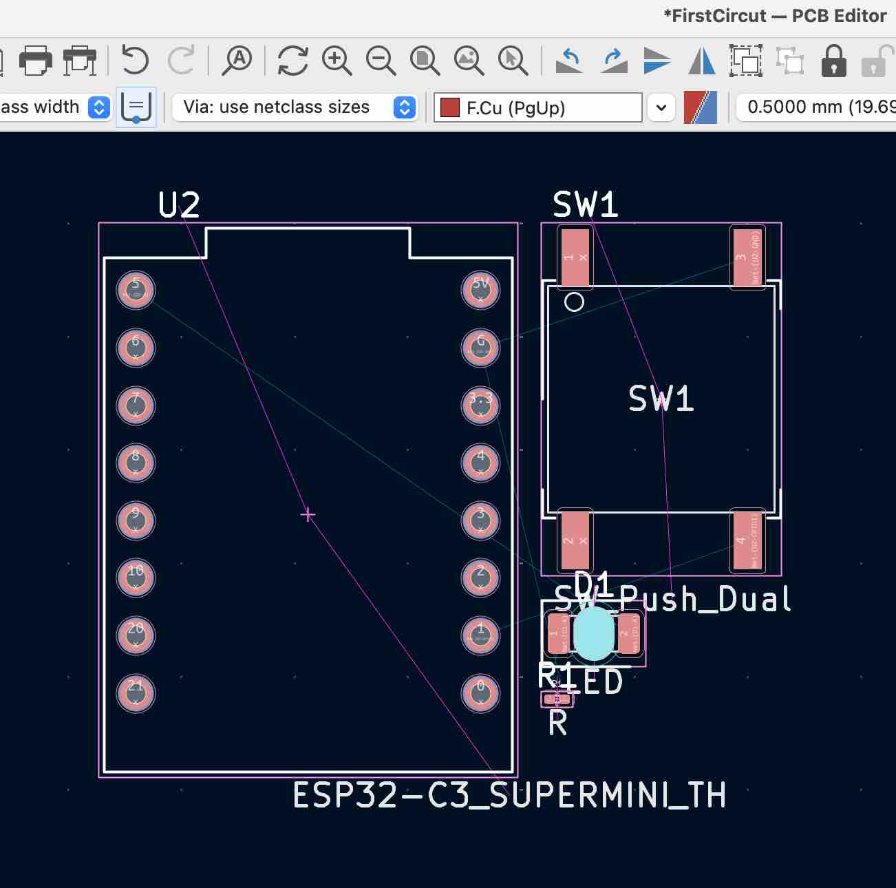
11 | This is how it looks, and I found that I had selected the wrong LED and resistor part. So I had to switch back to the Schematic editor and repeat steps 4–10.
12 | So I had to switch to the schematics editor and repeat steps 4–10
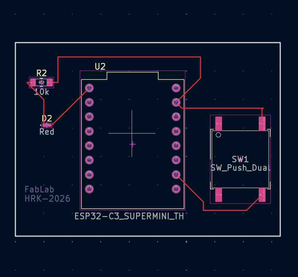
13 | This is how it looks in the PCB Editor with all routes connected
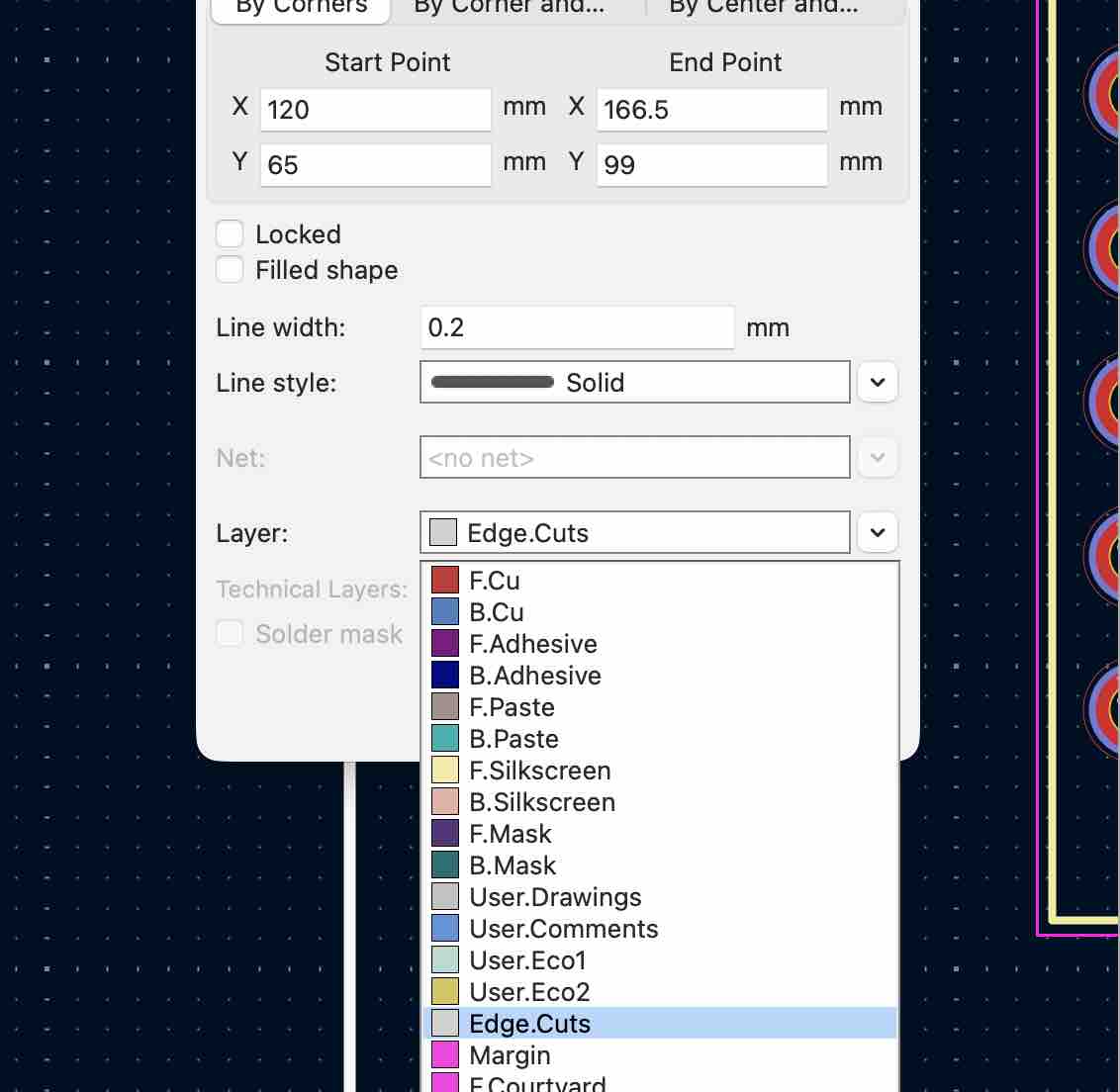
14 | I also drew the outline of the board and changed its layer property to Edge Cuts.
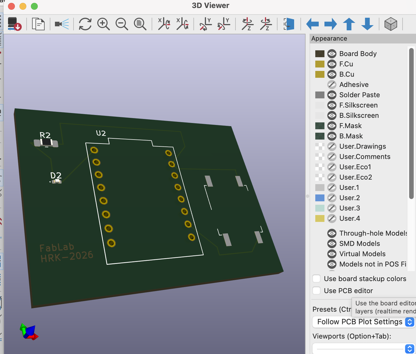
14 | and this is how it looks in the 3D Viewer
- Feedback: KiCad is an interesting EDA. It took me time to learn the basics, and fixing the errors took hours spent on tutorials. Even so, it's worth the effort.
- Challenge: Knowing the exact name of the parts in the library and making sure each has a footprint to be linked to. Many library parts are missing footprints.
04: Design a case in FreeCAD
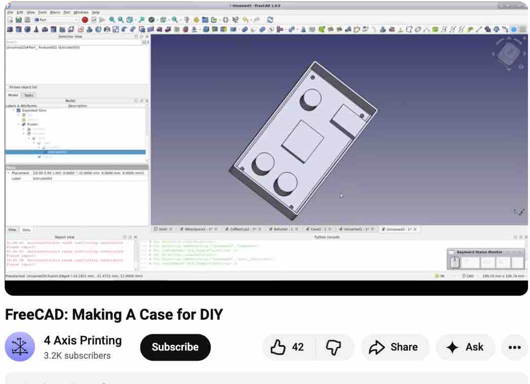
00 | I followed this YouTube tutorial
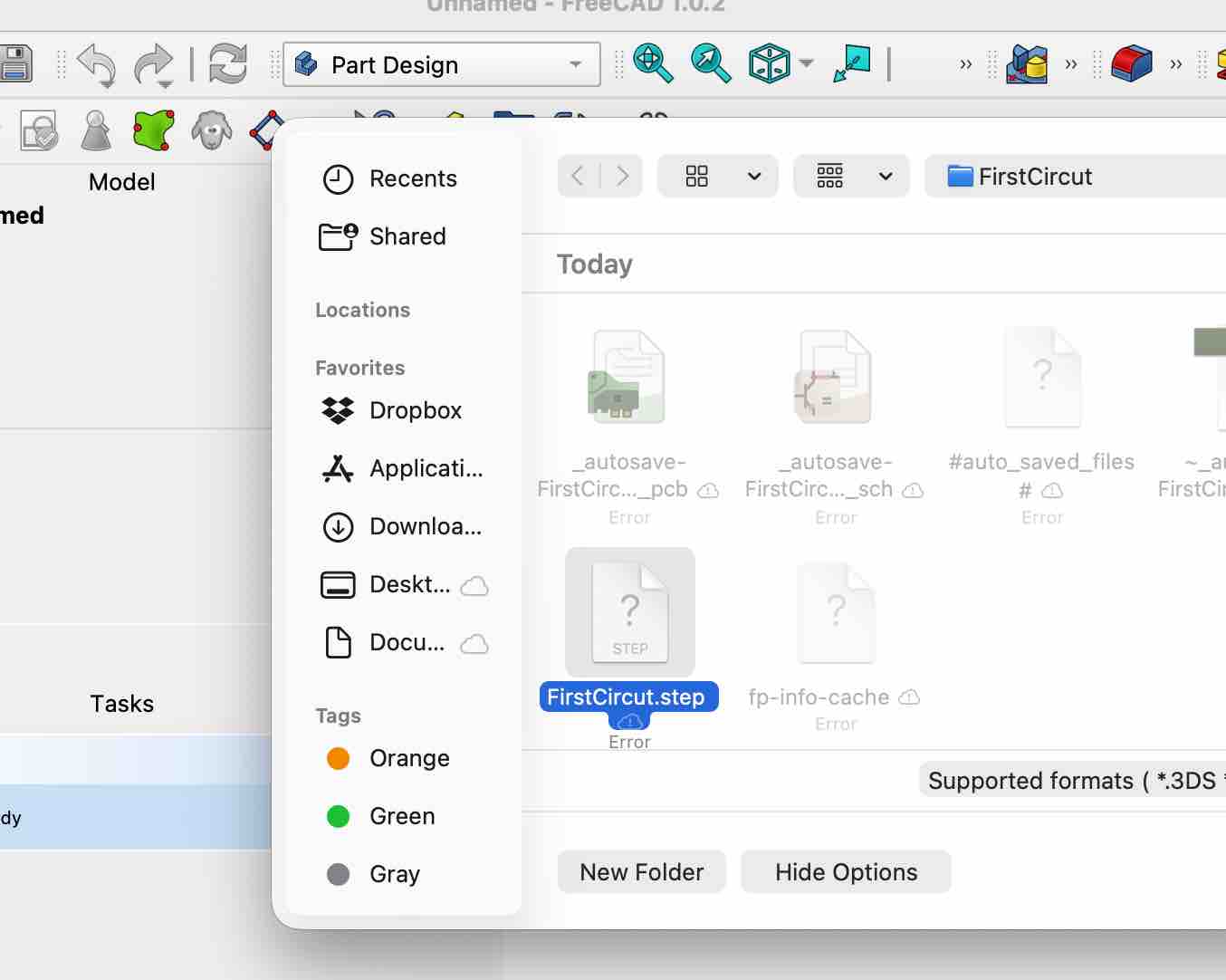
01 | I exported my KiCAD file as STEP file, Imported it to the FreeCAD and started creating the case
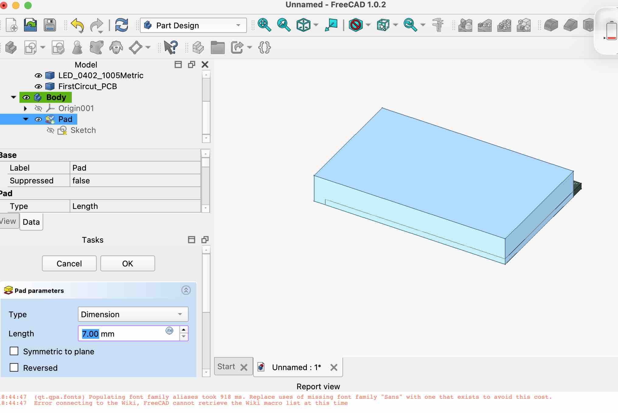
02 | I followed the steps in the video to create a case
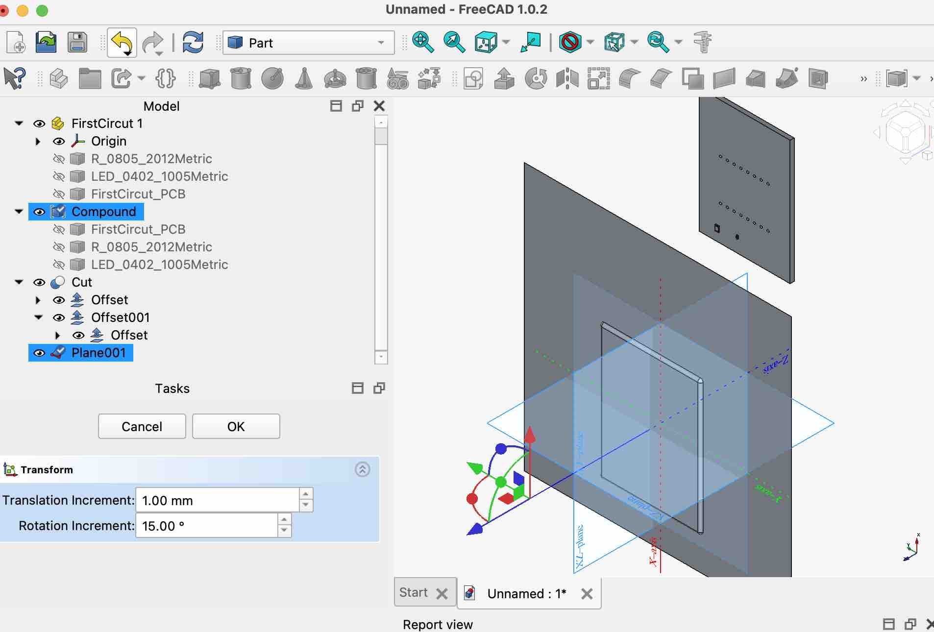
03 | I was not able to complete slicing the top cover of the case, and I ran out of time to complete this task
- Feedback: I learned a lot and I appreciate parametric designs for the case — it was very easy and time-saving compared to the previous way I used to manually try to fit things in
- Challenge: Time, time, time… I need more time to watch tutorials and try more. Sometimes I feel I didn't try enough to even ask for assistance