Group assignment: Electronics Production
During this group assignment, we characterized the electronics production workflow at Fab Lab Puebla by comparing two key technologies: mechanical milling and laser ablation. Through this process, we gained hands-on experience with the Roland MonoFab SRM-20 and the xTool F1 Ultra, allowing us to define the specific design rules and tolerances required for reliable PCB fabrication.
Key learnings include:
- Machine Characterization: We performed clearance and width tests using Neil’s trace files to determine the physical limits of our tools, achieving precise traces down to 0.1 mm.
- Software Workflow: We mastered the use of Mods to generate RML toolpaths for the Roland milling machine and xTool Creative Space for laser calibration and engraving.
- Technology Comparison: We analyzed the advantages of CNC milling for traditional FR-1 PCBs versus the high speed and dual-source (fiber/diode) versatility of laser processing for marking and cutting.
- Industrial Outsourcing: We also explored the workflow for sending designs to a board house (JLCPCB), learning how to correctly configure Gerber files and manufacturing parameters.
Electronics Production - Assignment
This week was dedicated to the physical realization of my circuit designs. I transformed a digital schematic into a tangible, high-precision PCB by utilizing specialized CNC milling techniques, focusing on trace isolation and structural accuracy for embedded systems.
The manufacturing process was performed on a single-sided copper phenolic substrate. To ensure the reliability of the electrical paths and the fit of the components, I implemented a multi-stage machining strategy using specific tooling:
- Tooling Strategy: I configured the job using three distinct bits: a 45° V-bit for defining the signal traces, a 0.4 mm drill bit for through-hole vias, and a 2 mm end mill for the final board perimeter.
- G-code Generation: I processed the design files to establish precise toolpaths, adjusting the isolation width to prevent short circuits between the copper pads.
- Substrate Fixation: I applied high-bond double-sided tape to secure the phenolic board to the machine bed, eliminating any surface vibration that could compromise the milling depth.
- Z-Axis Calibration: I performed a meticulous zeroing process for each tool change. For the V-bit, this calibration is vital to maintain a consistent trace width of approximately 0.4mm.
- Isolation Routing: The first pass involved the V-bit engraving the isolation paths, effectively stripping the copper layer to create the circuit's logic.
- Drilling and Contouring: After the traces were cleared, I executed the drilling cycle for component leads and finished with a profile cut to release the board from the stock material.
- Surface Preparation: Once the milling was completed, I deburred the edges and polished the traces with a fine abrasive pad to ensure optimal solder adhesion.
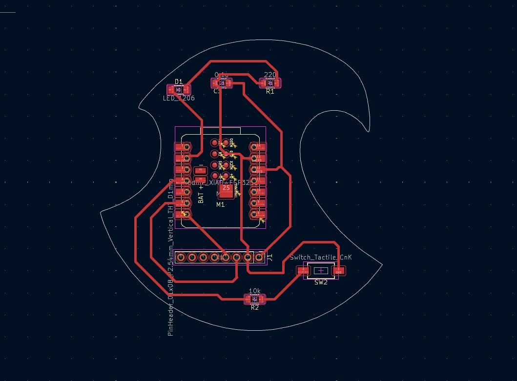
Gerbers
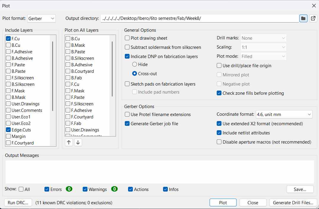
Once the PCB routing is finalized in KiCad’s PCB Editor, the next critical step is the generation of fabrication outputs. For our specific manufacturing process, we must export the design as Gerber (RS-274X) files. This involves using the 'Plot' menu to select the necessary layers—such as F.Cu (Front Copper), B.Cu (Back Copper), and Edge.Cuts (Board Contour). These files, combined with the generated Drill files (.drl), serve as the primary input for the machining software to define where the copper should be removed and where the mounting holes should be placed.
1. Layout Optimization: I updated the PCB design originally created in Week 06. The goal was to consolidate the traces and components to minimize the copper footprint and avoid material waste.
2. Exporting Fabrication Files: Once the layout was finalized, I navigated to File > Fabrication Outputs > Gerbers (.gbr) to prepare the vector data for the manufacturing software.
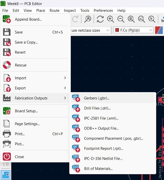
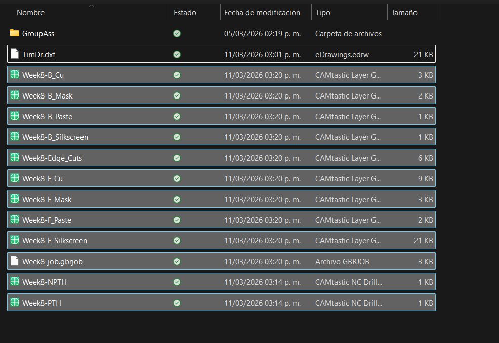
3. Output Directory: I selected a dedicated project folder for the output. It is important to keep the drill files and layer plots together for the next conversion step.
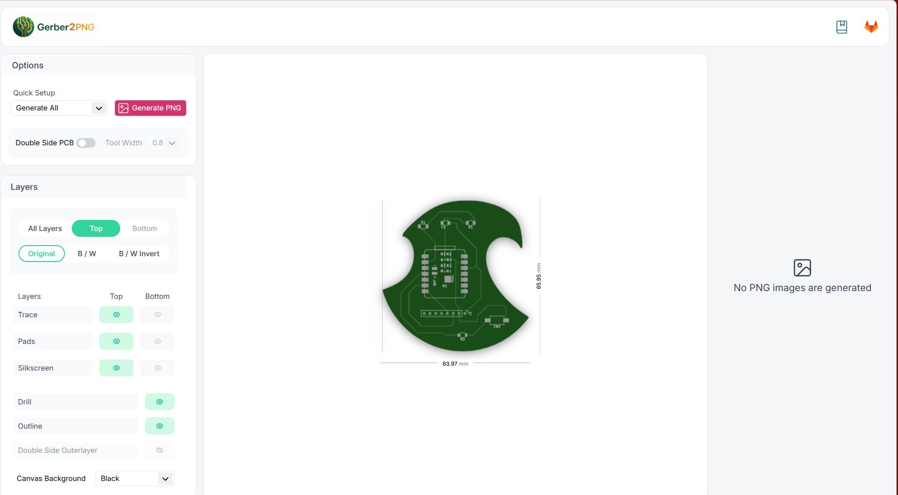
4. Format Conversion: I used the Gerber2png web tool to transform the vector files into high-resolution raster images required by the milling software.
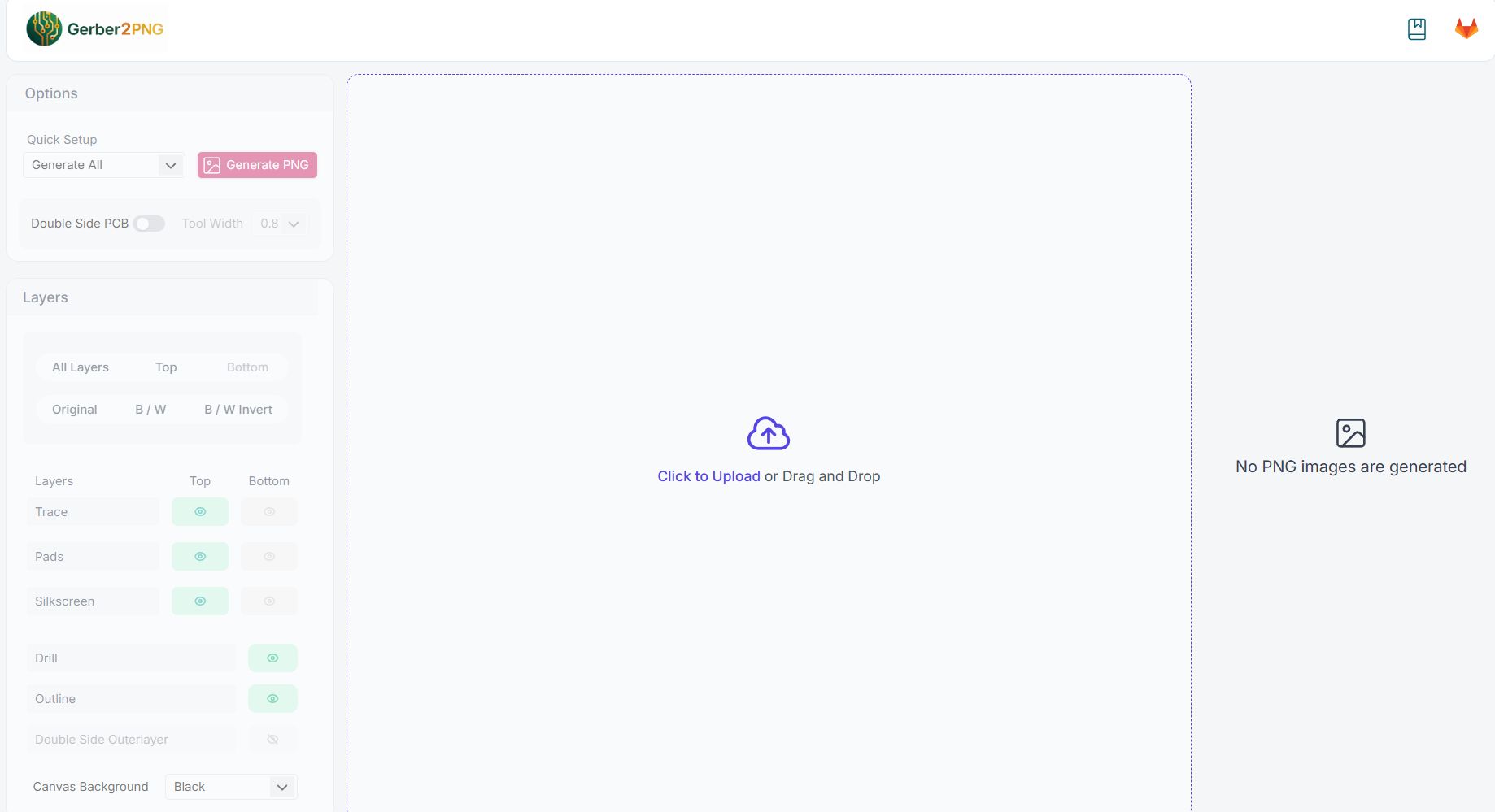
5. Batch Uploading: I uploaded all the generated Gerber files simultaneously. The tool automatically identifies which files correspond to traces, drills, and the board edge.
6. Digital Preview: A real-time preview of the PCB layers is generated. This step is crucial to verify that the trace clearances and hole positions align correctly with the design intent.
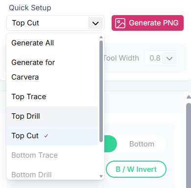
7. PNG Generation: Using the Quick Setup, I generated specific PNG files for each machining stage: Traces (Isolation), Drills (Through-holes), and the Cut (Edge.Cuts).
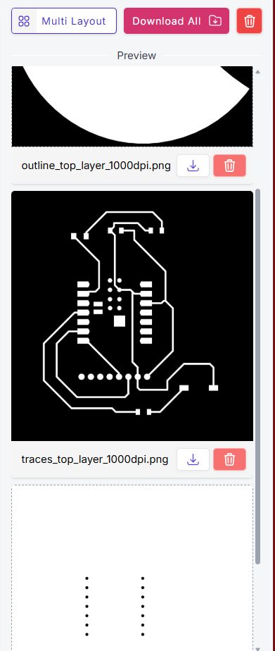
8. Final Assets: Finally, I downloaded the complete set of high-resolution images. These files are now ready to be processed into toolpaths for the precision milling machine.
Mods
The transition from a digital KiCad layout to a physical board is managed through MODS CE. This open-source tool is essential for generating the G-code required by our machining hardware. The process involves loading the high-resolution Gerber files or SVG exports from KiCad into the MODS workspace, where we define the 'mill traces' or 'mill outline' operations. This stage is critical because it calculates the necessary offsets to account for the physical width of the milling bit, ensuring that the final traces on the copper-clad board maintain their intended electrical clearance and structural integrity.
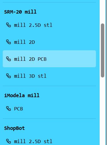
1. Accessing Mods CE: I used the Mods Community Edition interface to process the images. The first step is to navigate to the 'Programs' tab to select the appropriate server-side node configuration.
2. Machine Selection: I selected the 'Mill 2D PCB' program. This node-based workflow is specifically designed to handle raster-to-G-code conversion for precision milling machines.
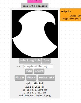
3. Loading the PNG: I uploaded the high-resolution PNG file generated in the previous stage. The software uses the pixel data to distinguish between the copper (white) and the material to be removed (black).
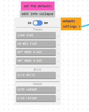
4. Toolpath Configuration: I defined the machining strategy based on the operation. For traces, I used the 'PCB traces (1/64)' preset, which automatically adjusts the cut depth and offsets for isolation routing.
5. Calculating Offsets: I verified the tool diameter (e.g., 0.4mm for a V-bit) and the number of offsets. Clicking 'Calculate' generates a 2D preview of the actual path the tool will follow.
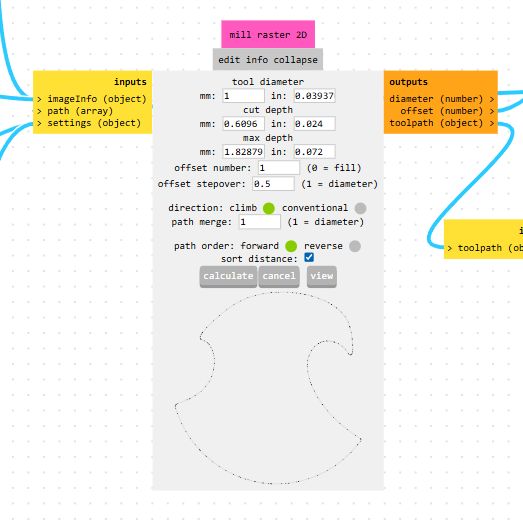
6. Origin Alignment: It is critical to ensure that the Origin (X0, Y0, Z0) is correctly set in the 'Mill Raster 2D' node. This defines the starting point relative to the machine's physical workspace.
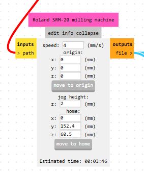
7. Saving the Toolpath: After enabling the 'Save file' node, I recalculated the path. This triggers a download of the .rml or .nc file, containing the specific instructions for the CNC controller.
PCB Machining
The fabrication phase represents the critical transition from digital electronic design to a functional physical prototype. For this project, we employ CNC (Computer Numerical Control) machining, a subtractive manufacturing process that offers high precision and rapid turnaround for double-sided or single-sided boards. Unlike traditional chemical etching, CNC milling provides a cleaner, mechanical approach to creating circuit traces by precisely removing the unwanted copper from the substrate. This section outlines the workflow used to translate our KiCad layouts into physical hardware, focusing on the generation of high-fidelity toolpaths and the configuration of machining parameters to ensure electrical reliability and structural integrity.
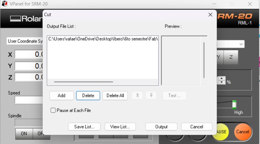
1. Machine Interface: I synchronized the hardware with the VPanel for SRM-20 software. This interface allows for manual control of the spindle and real-time monitoring of the coordinates.
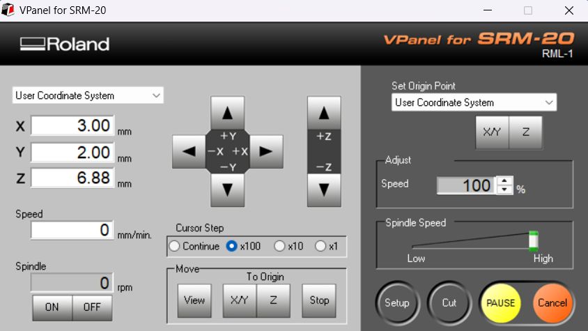
2. Setting the Origin: I manually jogged the machine to the starting corner of the board. I set the X/Y and Z origins using the 'Set Origin Point' button to establish the Work Coordinate System (WCS).
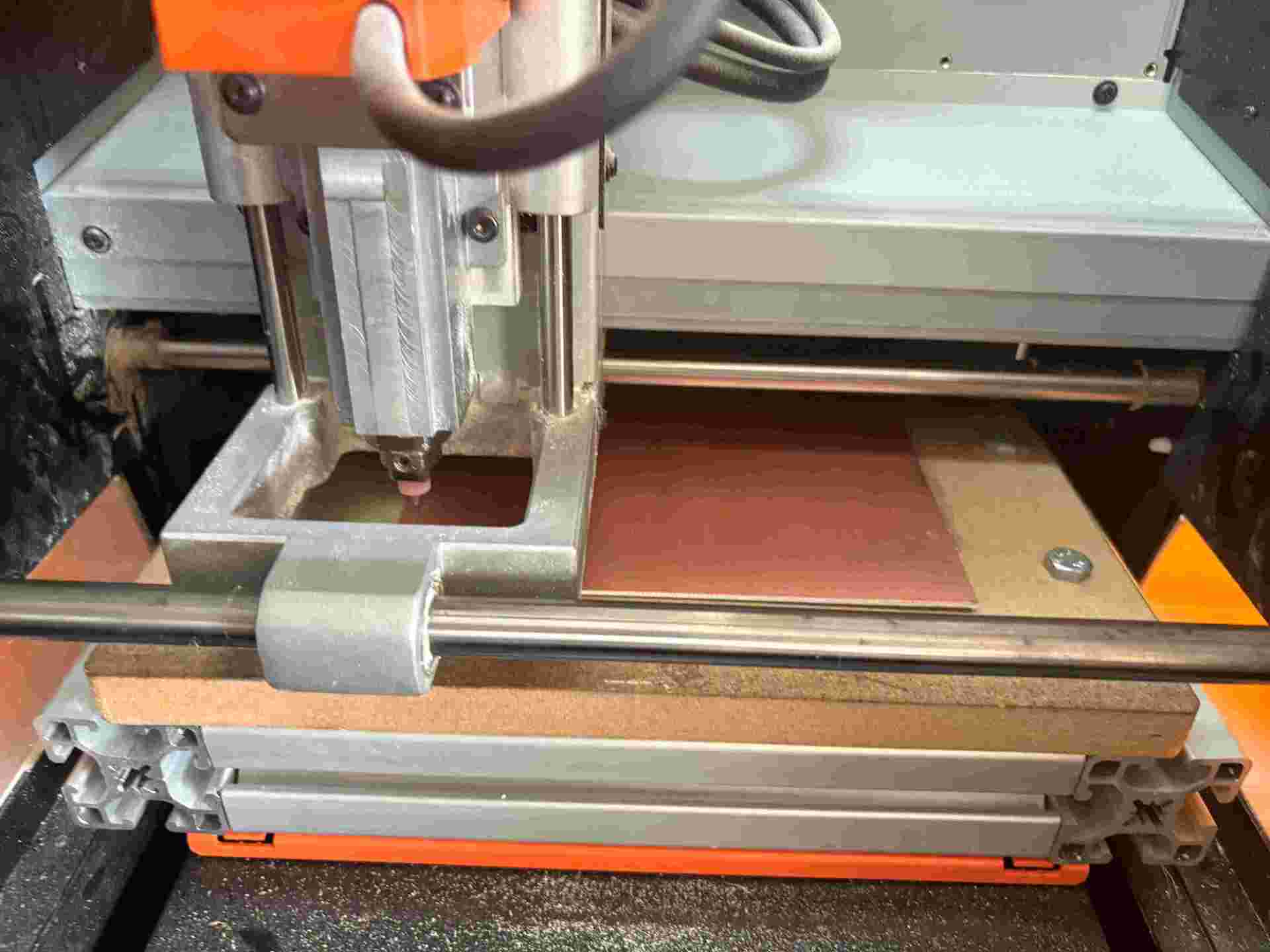
3. Executing the Job: Under the 'Cut' menu, I queued the files generated by Mods CE. Following the standard workflow, I processed the Drills first, followed by the Traces, and finally the Edge Cut.
5. In-Situ Inspection: Once the milling was finished, I inspected the traces before removing the board. This ensures that all isolation paths were fully cleared and there are no copper bridges.
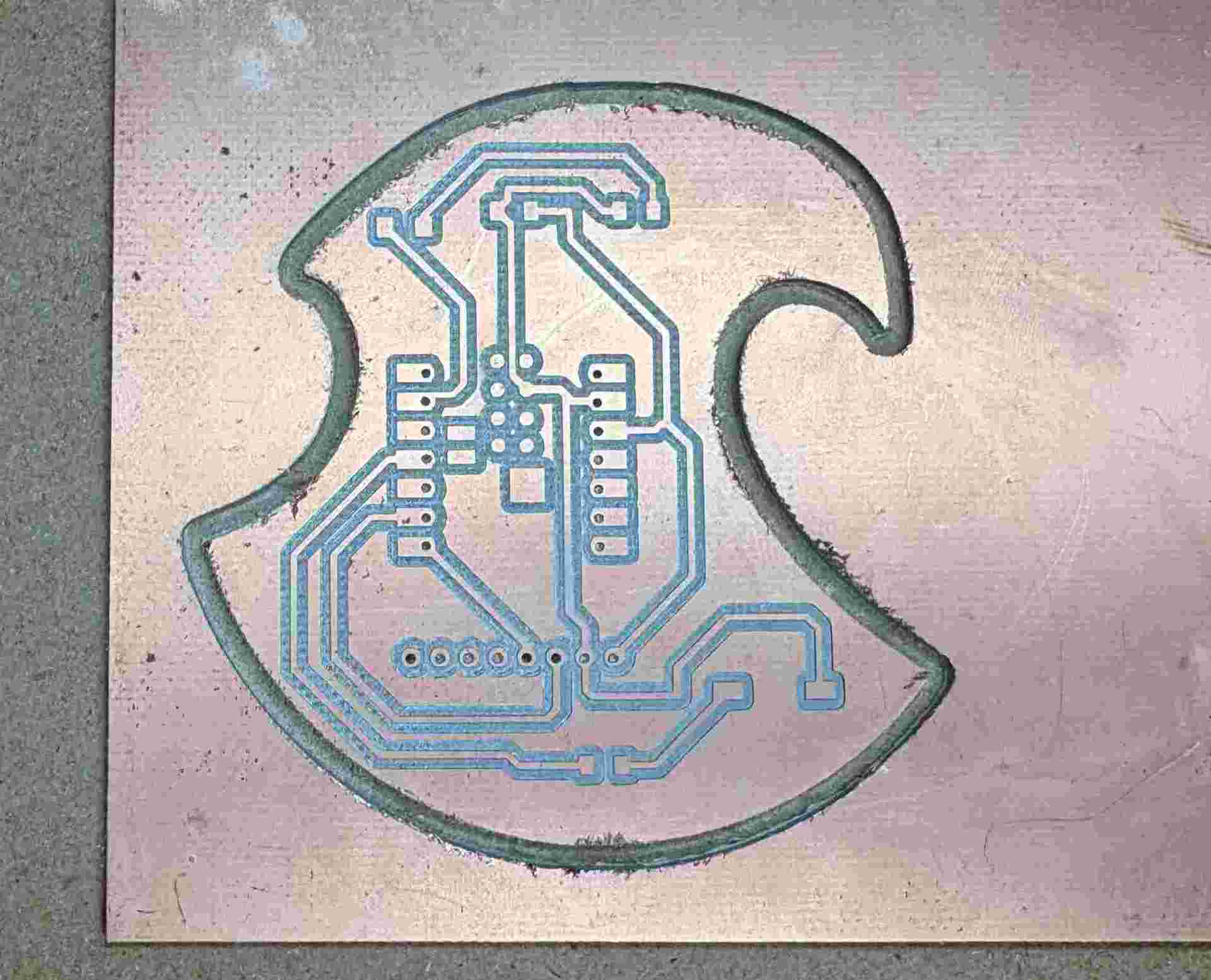
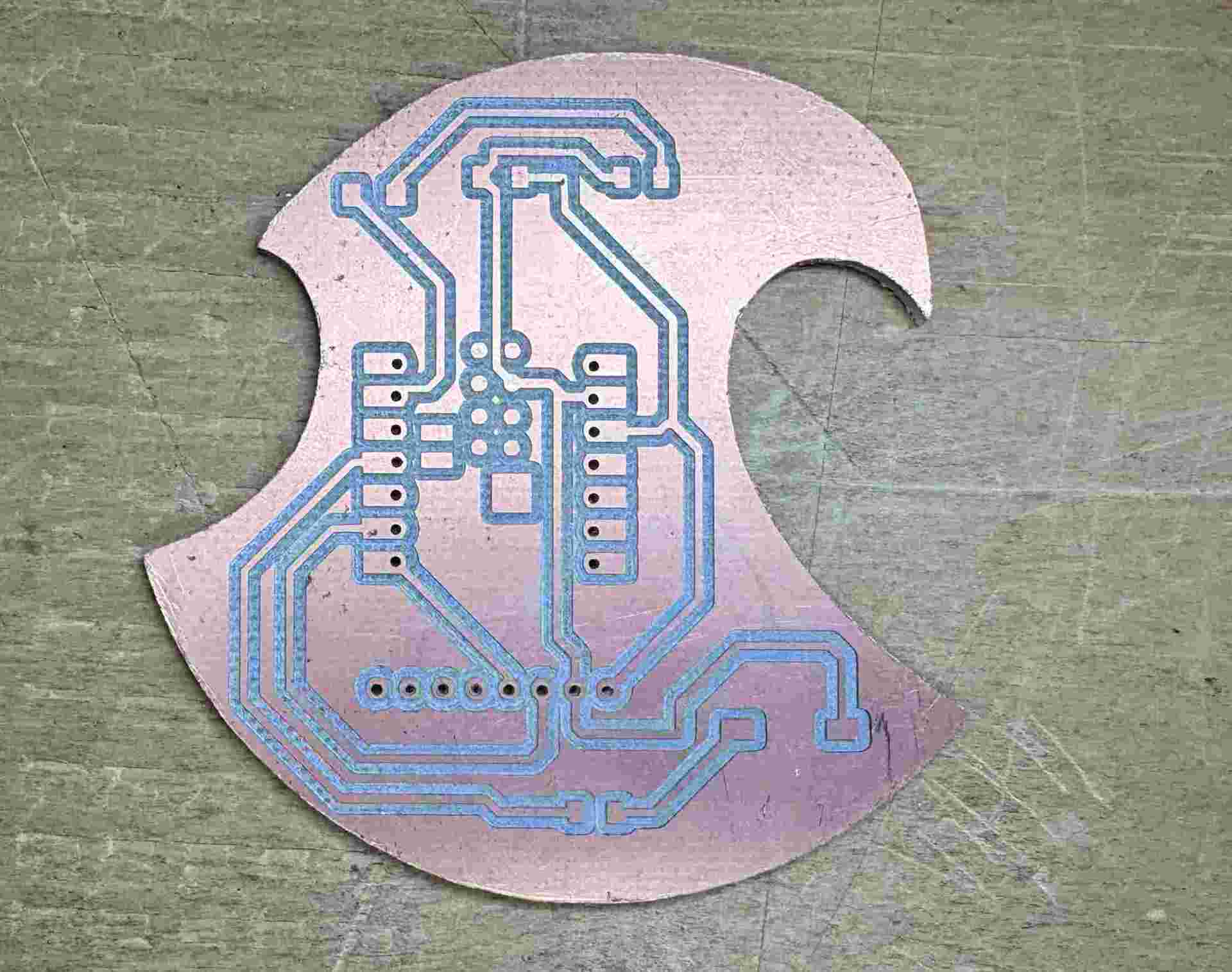
Finished Raw Board: The PCB was extracted and cleaned. The result shows sharp, defined tracks and clean drill holes, ready for the assembly phase. I verified the continuity of the traces to ensure no shorts were created during the milling process.
Important: Material Awareness & Safety
Upon reviewing my PCB fabrication, it was correctly pointed out that I am using FR-4 (Fiberglass-Reinforced Epoxy), recognizable by its greenish translucent substrate. It is vital to acknowledge that milling this material requires extreme caution.
Safety Warning: Unlike FR-1, the dust generated from FR-4 contains microscopic glass fibers. These particles are hazardous; they can penetrate the skin and, more dangerously, remain trapped in the lungs if inhaled, posing long-term health risks such as respiratory issues.
Context and Mitigation: Currently, FR-4 is the only material available in my local environment for the upcoming assignments. Since I will continue to use this stock for the rest of my boards, I have established a strict safety protocol to handle it consciously:
- Immediate Dust Control: Using a vacuum system during milling and performing a wet-clean of the machine bed afterwards to avoid fiber suspension.
- Skin Protection: Handling the raw material and debris with gloves to prevent fiberglass penetration.
Acknowledging these risks is part of my technical growth, ensuring that while I work with available resources, I do so with professional awareness and safety standards.
Bill of Materials (BOM)
Below is the list of components required to assemble the custom PCB, including the SMD parts and the connectors for the microcontroller and sensors.
| RefDes | Qty | Value / Type | Footprint | Description |
|---|---|---|---|---|
| D1 | 1 | LED | 1206 (SMD) | Visual indicator for motion modes. |
| R1 | 1 | 220 Ω | 1206 (SMD) | Current limiting resistor for LED D1. |
| C1 | 1 | 10uF / 100nF | 1206 (SMD) | Decoupling capacitor for power stability. |
| R2 | 1 | 10k Ω | 1206 (SMD) | Pull-up resistor for the tactile switch. |
| SW2 | 1 | Tactile Switch | SMD Push Button | Mode toggle button (Normal / Inverted). |
| M1 | 1 | Seeed XIAO ESP32C3 | XIAO TH Footprint | Main microcontroller unit. |
| J1 | 1 | Female Header 1x8 | 1mm Pitch | Connector for MPU-6050 / MPU-9250. |
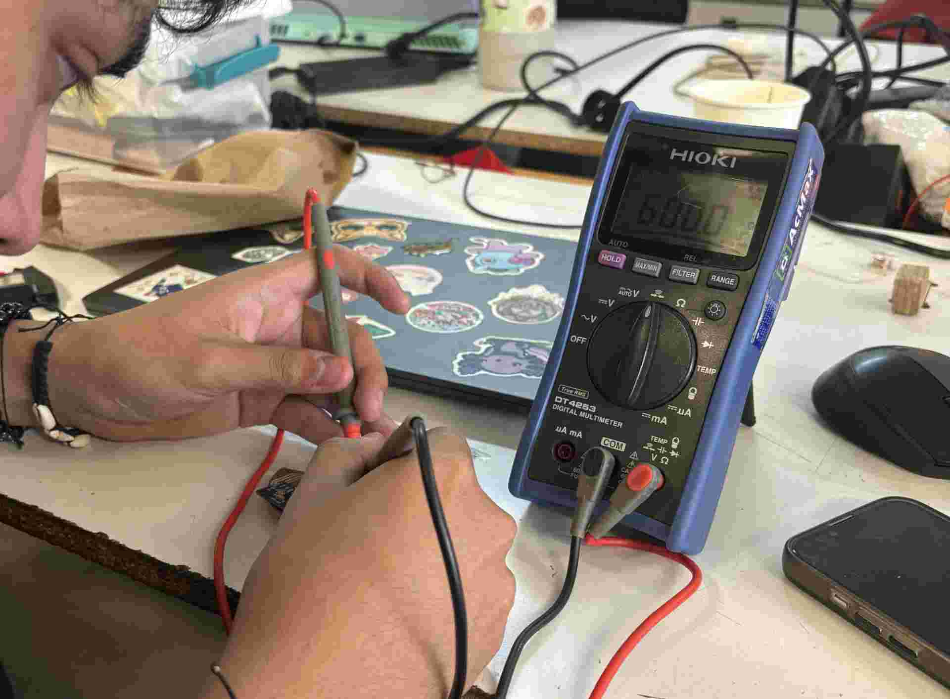
Pre-Assembly Validation: Continuity Testing
Before proceeding to assembly or powering the board, it is mandatory to perform a continuity check. Using a digital multimeter in continuity mode (beep test), I inspected the following:
- Trace Integrity: I verified that each path flows from start to finish without any micro-fractures in the copper.
- Short-Circuit Prevention: I checked for unintended bridges between adjacent tracks and, most importantly, between VCC and GND.
- Vias and Pads: I ensured that the drill holes were clean and that the copper rings were intact to provide a solid soldering surface.
Note: Detecting a short-circuit at this stage is much easier to fix with a craft knife than after the components have been soldered.
Final Assembly: I performed the soldering process, starting with the low-profile surface-mount components (SMD) and ending with the larger headers. The final result is a functional, custom-made microcontroller system.
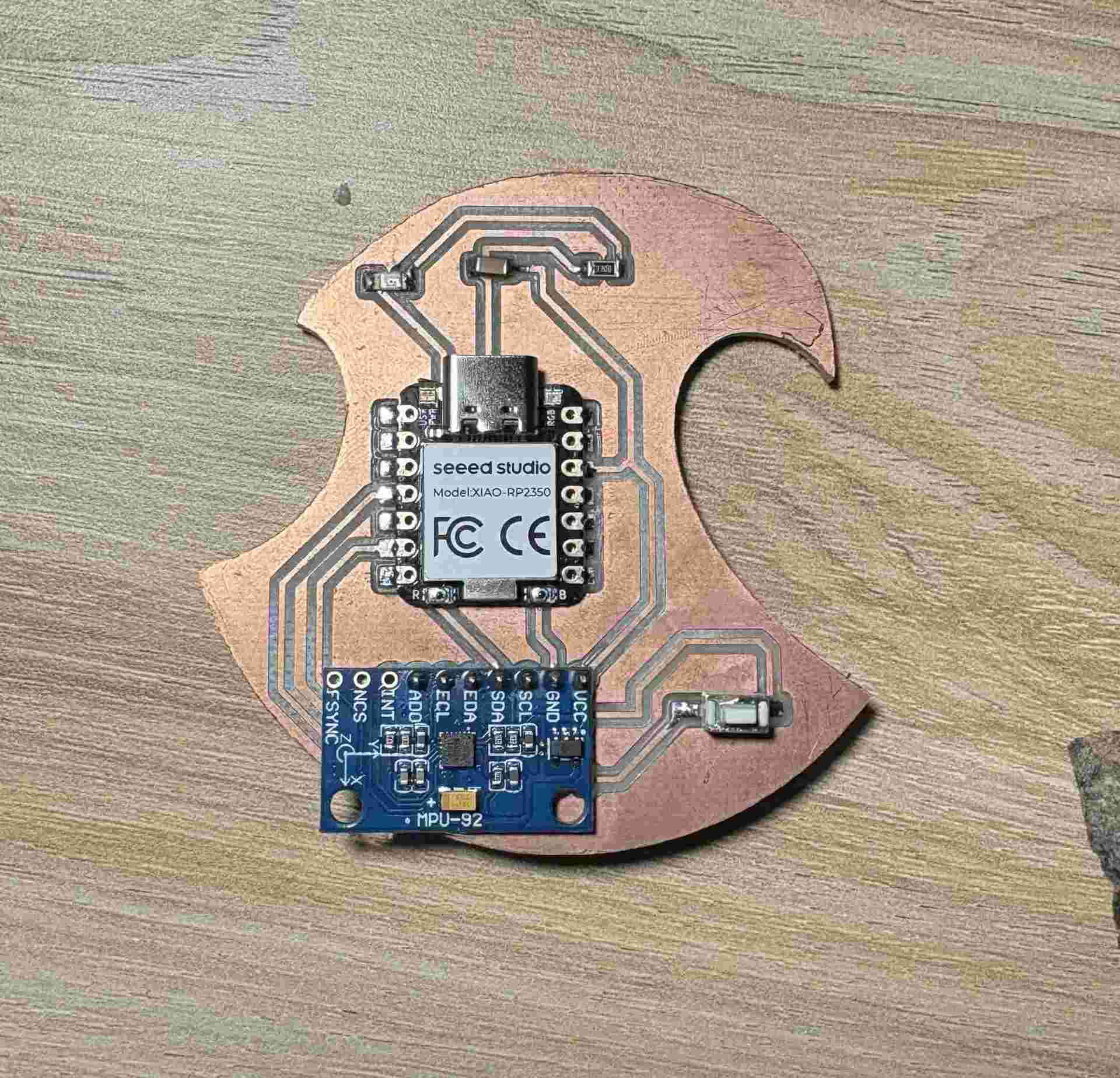
PCB Operation: The "LED ROBIN" Logic
For this custom PCB—inspired by the Red Robin (Tim Drake) logo—I developed a firmware that processes real-time inertial data to trigger visual alerts. The system centers around the "LED ROBIN": a reactive LED that changes its behavior based on the board's orientation and acceleration.
Validation of Original Design: This logic follows the exact functional specifications I originally designed and tested during the Week 04 simulation in Wokwi. Successfully replicating this behavior in the physical PCB confirms that the project's primary objective—transitioning from a virtual prototype to a functional embedded system—was fully achieved.
The core logic uses the MPU-9250 to calculate the combined magnitude of the three acceleration axes ($|ax| + |ay| + |az|$). I set a specific Threshold (22,000) that accounts for the gravity vector. When the board is tilted, the gravitational force shifts across the axes, causing the magnitude to exceed the limit and trigger a "Peak Event":
- Normal Mode: The LED remains OFF when the board is flat on the table (Static/Horizontal). If the board is tilted or inclined, the magnitude stays above the threshold and the LED remains ON until the board is returned to its horizontal position.
- Inverted Mode (Robin Mode): By pressing the physical button, the logic is flipped. The LED remains ON while horizontal. Once the board is tilted or moved, the magnitude triggers the threshold and the LED turns OFF, staying dark as long as the inclination persists.
This implementation effectively uses the accelerometer not just for motion, but as a tilt-switch, demonstrating how gravity influences sensor data acquisition through a manual I2C Bit-Banging protocol.
Troubleshooting & Debugging: The I2C Pinout Error
After assembling the board, I encountered a critical hardware conflict during the initial firmware upload. This section documents the diagnostic process and the software-based solution implemented to bypass a physical routing mistake without re-manufacturing the PCB.
- The Mistake: During the PCB design phase, I incorrectly assigned the I2C pins. I routed SDA to D6 (GPIO 28) and SCL to D5 (GPIO 27) on the XIAO RP2350, assuming any digital pin pair could initialize the standard
Wirelibrary. - The Technical Issue: The RP2350 architecture features two independent hardware engines: I2C0 and I2C1. GPIO 27 (D5) belongs to the I2C1 block, while GPIO 28 (D6) belongs to I2C0. The standard hardware library requires both pins to share the same internal peripheral engine.
- The Symptom: Every time
Wire.begin()was called, the processor attempted to synchronize incompatible hardware blocks, causing it to "hang" or enter a continuous reboot loop, resulting in a loss of Serial Monitor communication. - The Solution (Bit-Banging): To resolve this, I implemented Software I2C (Bit-Banging). This method manually toggles the GPIO states (High/Low) to mimic the I2C protocol timing, effectively creating a virtual I2C bus on any digital pin.
- Implementation: I developed a custom I2C script (Start, Stop, Write, and Read functions) that ignores the chip's hardware constraints and communicates directly with the sensor through manual signal manipulation.
- Verification & Success: The approach was successful. I managed to "ping" the MPU-9250 at address
0x68, confirming that the physical traces, power delivery, and pull-up resistors were correct despite the logical routing error.
Lesson Learned: Always consult the Processor Pinout Datasheet for peripheral multiplexing (MUX) before routing communication buses. Hardware-dedicated pins are not always interchangeable.
Programming
To bring the "LED ROBIN" logic to life, I used the Arduino IDE. You can install it directly from the Microsoft Store or download the latest version from the Official Arduino Page. Once the environment was ready, I followed these steps to configure the XIAO RP2350:
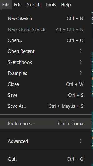
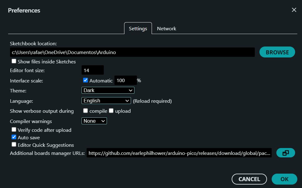
1. Environment Configuration: Open the Arduino IDE and navigate to File > Preferences. This is where we define the external repositories for non-native boards.
2. Adding Board Manager URL: In the "Additional Boards Manager URLs" field, copy and paste the following link to enable support for the RP2350 architecture:
https://github.com/earlephilhower/arduino-pico/releases/download/global/package_rp2040_index.json
(Click the link above to copy)
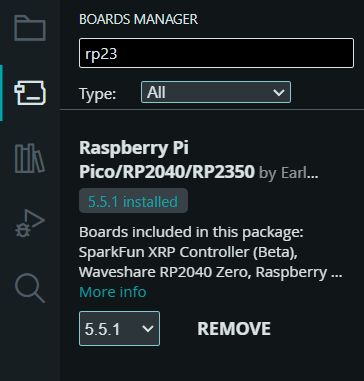
3. Installing Core Packages: Go to Boards Manager. Search for "Raspberry Pi Pico/RP2350" and install the latest version of the core library.
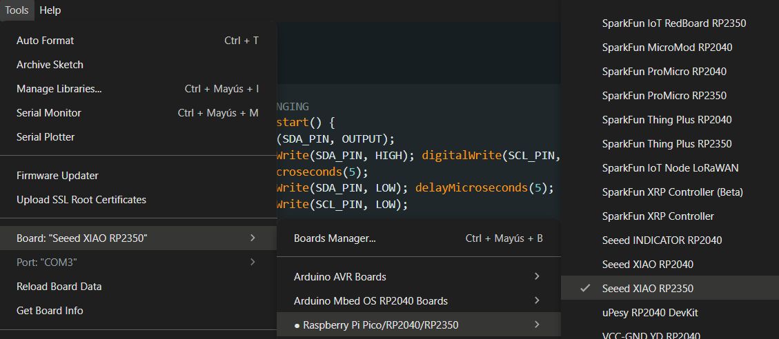
4. Hardware Selection: Navigate to Tools > Board > Raspberry Pi RP2350 Boards and specifically select the Seeed XIAO RP2350 to load the correct pinout definitions.
Code
Firmware Implementation: Software I2C (Bit-Banging)
Key Functional Features & Firmware Logic
The system's intelligence relies on a custom-written firmware designed to interface with the MPU-6050 via bit-banging and process real-time motion data.
- Manual I2C Implementation (Bit-Banging): Due to a mismatch in the hardware I2C pins, I developed custom low-level functions (
i2c_start,i2c_stop,i2c_write,i2c_read). These functions manually toggle the SDA and SCL lines to handle protocol timing and data transfer without relying on built-in libraries. - Motion Magnitude Calculation: The firmware retrieves raw acceleration data from the X, Y, and Z axes. To detect a general state of motion regardless of orientation, it calculates the total magnitude using the formula:
$|ax| + |ay| + |az|$
This sum is compared against a calibrated threshold of 22,000 units to trigger the system's response. - Dual Operating Modes:
- Normal Mode: The "LED ROBIN" activates only when motion or tilt exceeds the defined threshold.
- Inverted Mode: The LED remains active by default and switches OFF momentarily when movement is detected, creating a reactive visual feedback.
- State Management & Debouncing: A physical button toggles between operating modes in real-time. I implemented state-change detection logic to ensure that a single press only triggers one mode swap, preventing erratic behavior from mechanical button bounce.
- Reactive Feedback Timing: To ensure the visual alert is perceivable by the human eye, I included a retention timer (
TIEMPO_RETENCION). This keeps the LED state stable for 250ms after a motion peak is detected, preventing flickering.
        #define SCL_PIN D5
        #define SDA_PIN D6
        #define LED_ROBIN D1
        #define BUTTON_PIN D3
        #define MPU_ADDR 0x68

        // Sensibility
        long UMBRAL_MOVIMIENTO = 22000;
        const int TIEMPO_RETENCION = 250; // Time led is on

        bool logicaInvertida = false;
        bool ultimoEstadoBoton = HIGH;
        unsigned long ultimoPicoMs = 0;

        // BIT-BANGING
        void i2c_start() {
        pinMode(SDA_PIN, OUTPUT);
        digitalWrite(SDA_PIN, HIGH); digitalWrite(SCL_PIN, HIGH);
        delayMicroseconds(5);
        digitalWrite(SDA_PIN, LOW); delayMicroseconds(5);
        digitalWrite(SCL_PIN, LOW);
        }

        void i2c_stop() {
        pinMode(SDA_PIN, OUTPUT);
        digitalWrite(SDA_PIN, LOW); digitalWrite(SCL_PIN, HIGH);
        delayMicroseconds(5);
        digitalWrite(SDA_PIN, HIGH); delayMicroseconds(5);
        }

        bool i2c_write(uint8_t byte) {
        pinMode(SDA_PIN, OUTPUT);
        for (int i = 0; i < 8; i++) {
            digitalWrite(SDA_PIN, (byte & 0x80) ? HIGH : LOW);
            byte <<= 1; delayMicroseconds(5);
            digitalWrite(SCL_PIN, HIGH); delayMicroseconds(5);
            digitalWrite(SCL_PIN, LOW);
        }
        pinMode(SDA_PIN, INPUT_PULLUP);
        digitalWrite(SCL_PIN, HIGH); delayMicroseconds(5);
        bool ack = (digitalRead(SDA_PIN) == LOW);
        digitalWrite(SCL_PIN, LOW);
        return ack;
        }

        uint8_t i2c_read(bool ack) {
        uint8_t byte = 0;
        pinMode(SDA_PIN, INPUT_PULLUP);
        for (int i = 0; i < 8; i++) {
            digitalWrite(SCL_PIN, HIGH); delayMicroseconds(5);
            byte = (byte << 1) | digitalRead(SDA_PIN);
            digitalWrite(SCL_PIN, LOW); delayMicroseconds(5);
        }
        pinMode(SDA_PIN, OUTPUT);
        digitalWrite(SDA_PIN, ack ? LOW : HIGH);
        digitalWrite(SCL_PIN, HIGH); delayMicroseconds(5);
        digitalWrite(SCL_PIN, LOW);
        return byte;
        }

        void setup() {
        Serial.begin(115200);
        pinMode(LED_ROBIN, OUTPUT);
        digitalWrite(LED_ROBIN, LOW);
        pinMode(BUTTON_PIN, INPUT_PULLUP);
        pinMode(SCL_PIN, OUTPUT);
        pinMode(SDA_PIN, INPUT_PULLUP);

        delay(3000);
        Serial.println("--- LED ROBIN: Ultra-Sensitive Mode ---");

        i2c_start();
        i2c_write(MPU_ADDR << 1);
        i2c_write(0x6B);
        i2c_write(0);
        i2c_stop();
        }

        void loop() {
        // Button
        bool estadoActualBoton = digitalRead(BUTTON_PIN);
        if (ultimoEstadoBoton == HIGH && estadoActualBoton == LOW) {
            logicaInvertida = !logicaInvertida;
            Serial.println(logicaInvertida ? "MODO: INVERTIDO" : "MODO: NORMAL");
            delay(200);
        }
        ultimoEstadoBoton = estadoActualBoton;

        // Sensor
        i2c_start();
        i2c_write(MPU_ADDR << 1);
        i2c_write(0x3B);
        i2c_stop();

        i2c_start();
        i2c_write((MPU_ADDR << 1) | 1);
        int16_t ax = (i2c_read(true) << 8) | i2c_read(true);
        int16_t ay = (i2c_read(true) << 8) | i2c_read(true);
        int16_t az = (i2c_read(true) << 8) | i2c_read(false);
        i2c_stop();

        long magnitud = abs(ax) + abs(ay) + abs(az);

        // 3. Peaks detection
        if (magnitud > UMBRAL_MOVIMIENTO) {
            ultimoPicoMs = millis();
        }

        bool alertaActiva = (millis() - ultimoPicoMs < TIEMPO_RETENCION);

        // 4. LED
        if (!logicaInvertida) {
            // Normal Mode: Motion detected = LED ON
            digitalWrite(LED_ROBIN, alertaActiva ? HIGH : LOW);
        } else {
            // Inverted Mode: Motion detected = LED OFF
            digitalWrite(LED_ROBIN, alertaActiva ? LOW : HIGH);
        }

        delay(20);
        }
Real Life Working: LED ROBIN in Action
Normal Mode (Logic)
Inverted Mode (Robin Mode)
This week was an invaluable lesson in hardware validation and design resilience. Despite facing a routing error in the I2C pins for the XIAO RP2350, implementing a software-based bit-banging protocol allowed me to rescue the board and fulfill the 'LED ROBIN' project objectives. This experience not only strengthened my diagnostic and debugging capabilities but also demonstrated that a solid programming foundation can compensate for physical limitations, ultimately resulting in a functional system capable of processing real-time inertial data.
Files
└── Week8Files
    ├── Week8.kicad_pcb
    ├── Week8.kicad_pro
    ├── Week8.kicad_sch
    ├── Cut
    │   ├── drills_top_layer_1000dpi.png.rml
    │   ├── outline_top_layer_2.png.rml
    │   └── traces_top_layer_1.png.rml
    ├── gerber
    │   ├── Week8-B_Cu.gbr
    │   ├── Week8-B_Mask.gbr
    │   ├── Week8-B_Paste.gbr
    │   ├── Week8-B_Silkscreen.gbr
    │   ├── Week8-Edge_Cuts.gbr
    │   ├── Week8-F_Cu.gbr
    │   ├── Week8-F_Mask.gbr
    │   ├── Week8-F_Paste.gbr
    │   ├── Week8-F_Silkscreen.gbr
    │   ├── Week8-job.gbrjob
    │   ├── Week8-NPTH.drl
    │   └── Week8-PTH.drl
    └── png
        ├── drills_top_layer_1000dpi.png
        ├── outline_top_layer_2.png
        └── traces_top_layer_1.png