Electronics design - Assignment:
During Electronics Design week, we focused on creating a custom electronic board by designing the schematic and PCB layout, understanding how components connect and work together in a functional system.
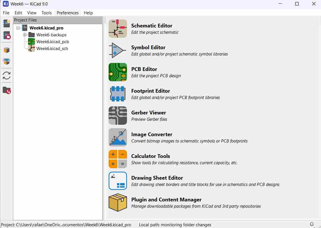
To start we need to download the program we will use, I used KiCad for this, entering follow some steps to get the library we need.
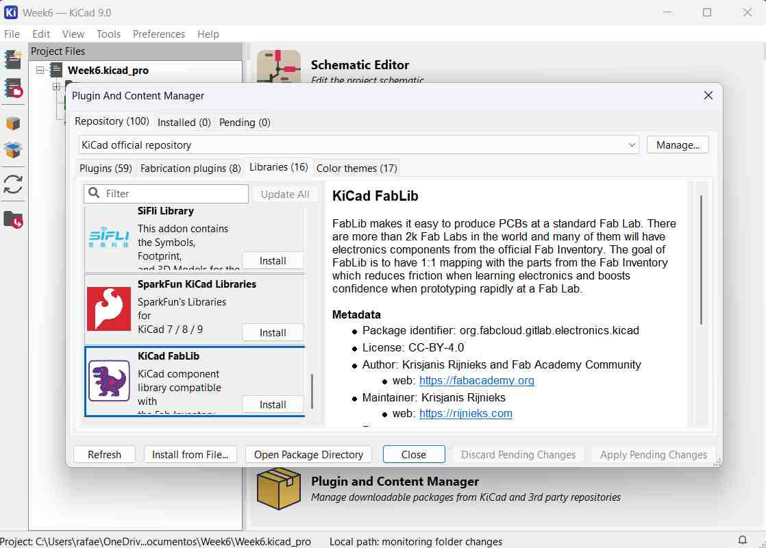
1. Accessing the Plugin Manager: Open KiCad and navigate to the Plugin and Content Manager. This tool allows you to manage external libraries and official community extensions.
2. Repository Search: Use the search bar to locate the KiCad Fablib. This specific library contains the standardized footprints and symbols required for Fab Academy projects. Click 'Install' to proceed.
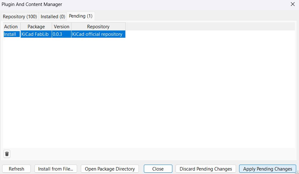
3. Confirming Changes: Navigate to the 'Pending' tab to review the selected libraries. Click on 'Apply Pending Changes' to synchronize the local repository with the new assets.
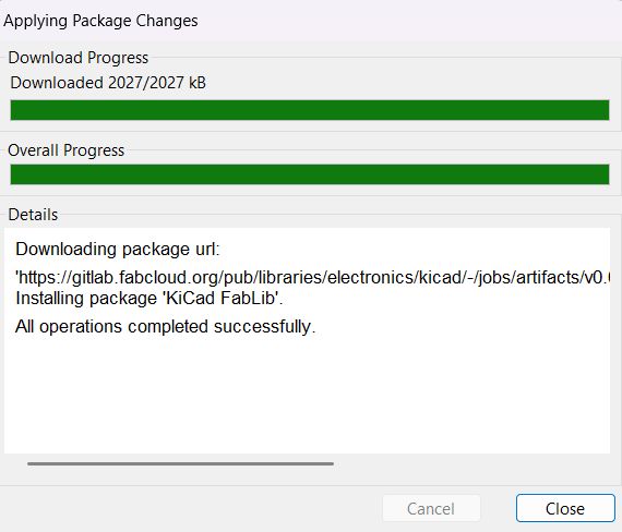
4. Installation Process: Wait for the downloader to fetch the library files and update the internal database. Once finished, the Fablib components will be available in the Schematic and PCB editors.
Circuit Design
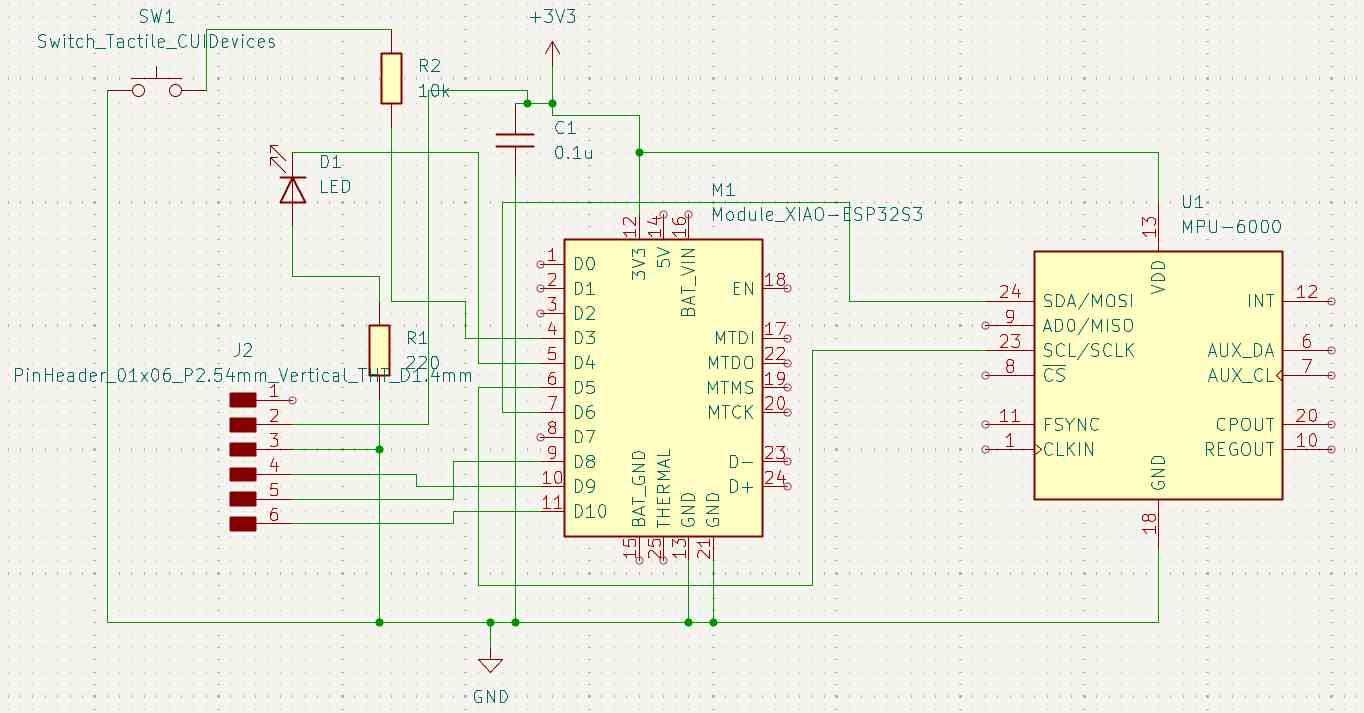
Once this is done, we can start to create our project. For my design I decided to reuse the idea of the circuit I did on my week 4, with the Xiao, just addding a pull-up button with the function of setting a origin for the accelerometer, for my simulation I considered a MPU but to replicate it I will use the libraries available on the Xiao.
1. Project Creation: Start by creating a new project in KiCad. This generates the necessary file structure for both the Schematic (.kicad_sch) and the PCB Layout (.kicad_pcb).
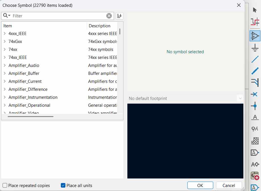
2. Symbol Selection: Use the 'Add Symbol' tool (hotkey 'A') to browse the libraries. Search for the components defined in your BOM, such as the XIAO nRF52840, resistors, and capacitors.
3. Component Placement: Place the symbols on the canvas. While you can move them later using the 'M' key, it is best practice to group related components (like decoupling capacitors) near their respective pins.
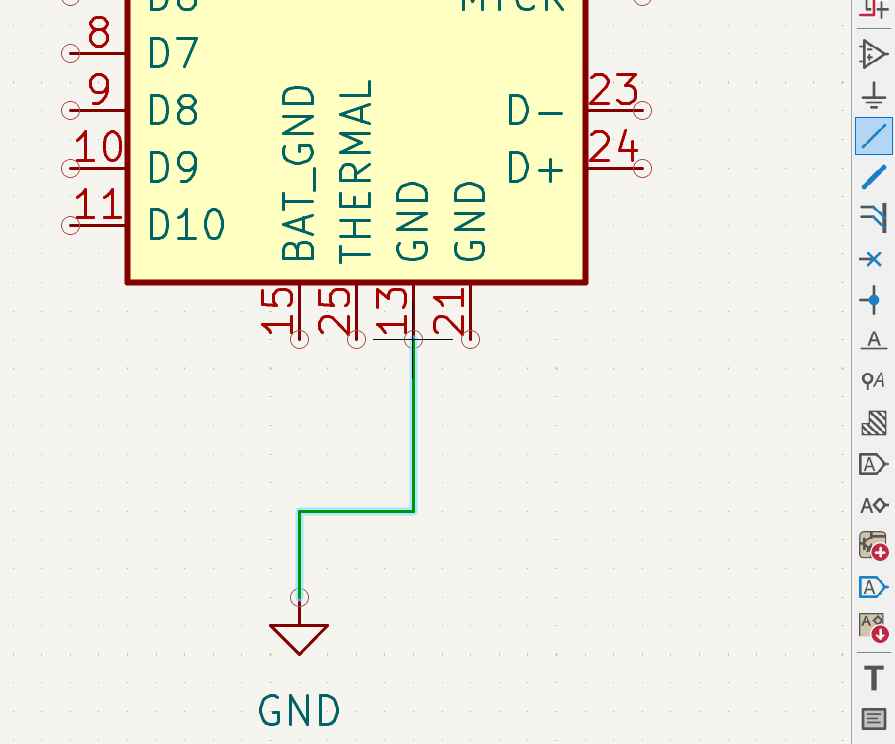
4. Wiring and Netting: Use the 'Add Wire' tool to establish electrical connections. Focus on creating a logical flow that clearly shows how the signals travel between the microcontroller and peripherals.
5. Programming Interface: Include a pin header section specifically for the programmer. This ensures you can easily upload firmware to the microcontroller once the board is fabricated.
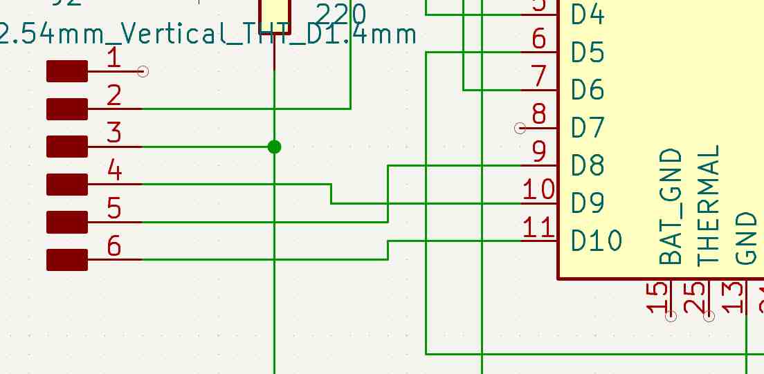
6. Schematic Verification: The final schematic should have clearly labeled nets and verified connections. Even if the layout looks complex, the priority is electrical accuracy and passing the Electrical Rules Check (ERC).
PCB Design
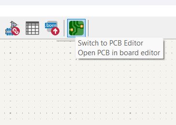
1. Switching to PCB Editor: Open the PCB Editor from the main project window to begin converting your schematic into a physical board layout.
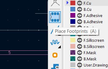
2. Footprint Management: While you can place footprints manually, the synchronization between the schematic and the layout is handled by the design rules.
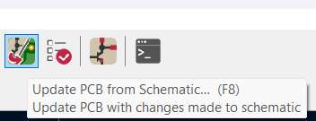
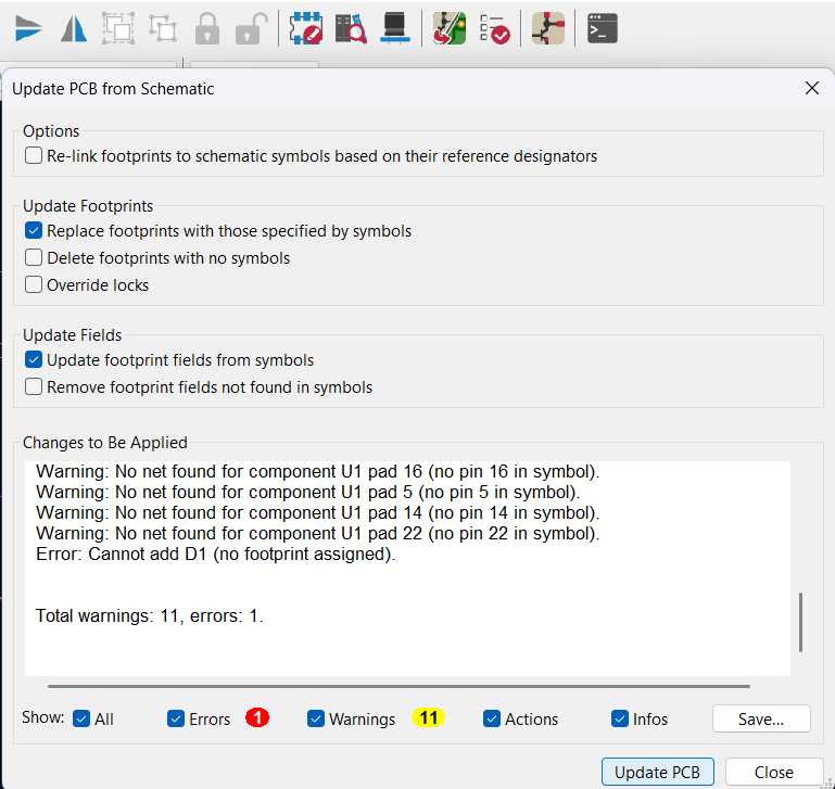
3. Update PCB from Schematic: This is the most efficient workflow. Use the 'Update PCB from Schematic' tool (F8) to import all components and net connections defined in your drawing.
4. Synchronizing Components: After clicking update, all footprints will appear attached to the cursor. Click to place the cluster on the workspace to begin the arrangement.
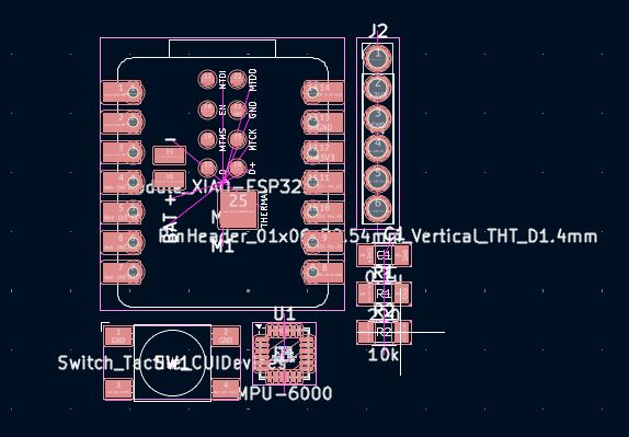
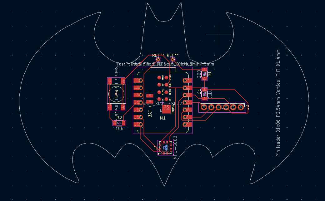
5. Component Placement: Arrange the components logically. Keep the microcontroller central and place bypass capacitors as close as possible to the power pins to reduce electrical noise.
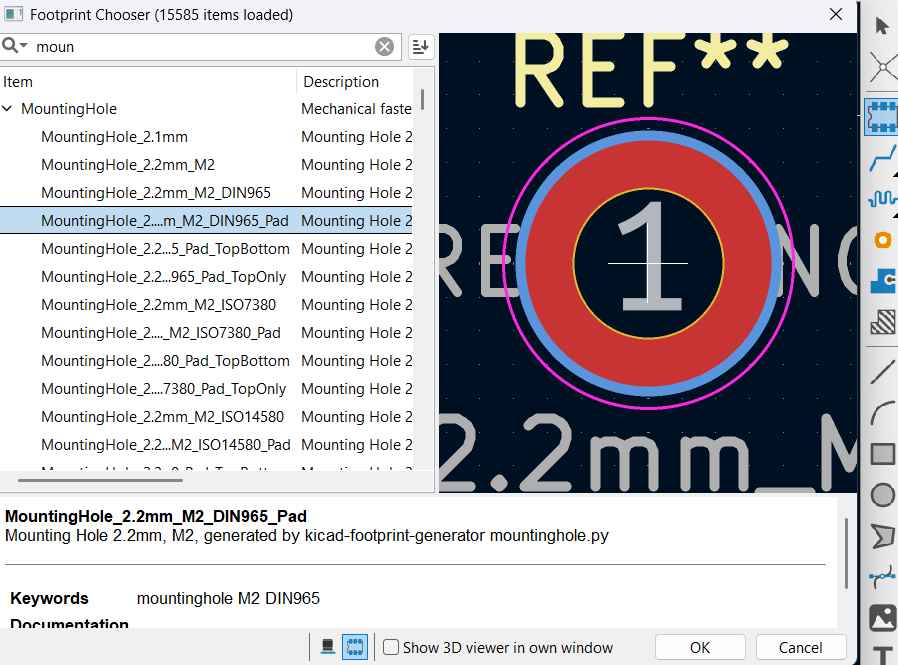
6. Mechanical Holes: For specific mounting requirements or larger LEDs, use the 'Mounting Hole' footprint. This ensures the physical board has the correct structural drillings.
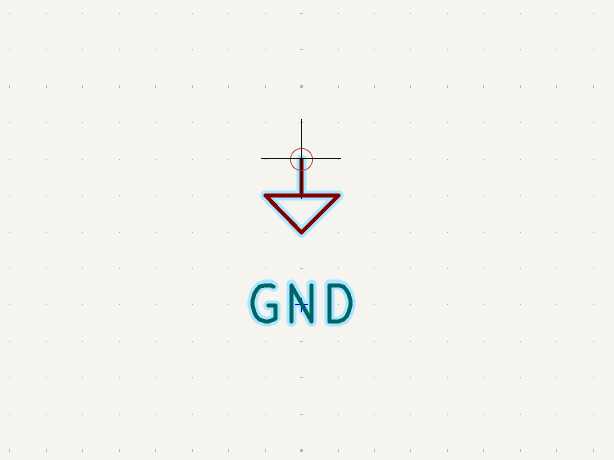
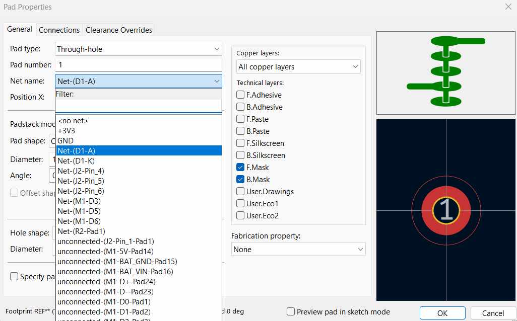
7. Assigning Nets: Ensure that any manual mechanical parts are assigned to the correct Net (like GND) so that the routing tool recognizes the electrical paths.
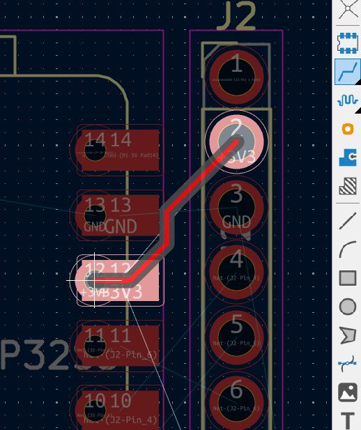
8. Routing Tracks: Use the 'Route Tracks' tool ('X') to draw the physical copper connections. Follow the "rat's nest" (thin lines) as a guide to complete all circuit paths.
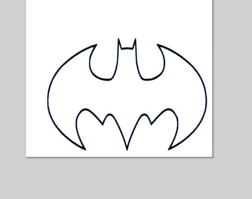
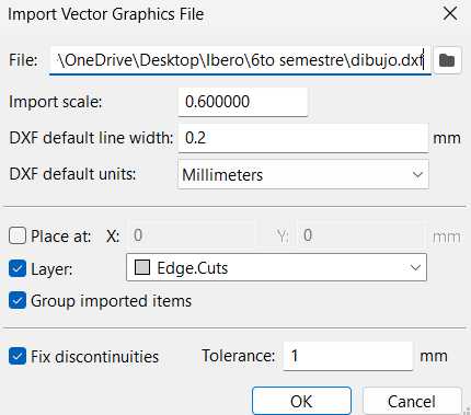
9. Custom Board Shape: To give the PCB a unique silhouette, I sourced the official logo from Google and processed it in a vector program. I then exported the final outline as a .DXF file to be imported into KiCad's Edge.Cuts layer.
10. Importing Graphics: Go to File > Import > Graphics. This allows you to bring your custom vector outline into the KiCad environment.
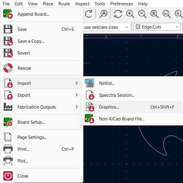
11. Edge Cuts Layer: Select the .DXF file and set the Graphic Layer to 'Edge.Cuts'. Ensure the scale is set to mm to maintain correct real-world dimensions.
12. Final Alignment: Center the Edge.Cuts geometry around your routed components. This boundary defines where the milling machine or factory will cut the board.
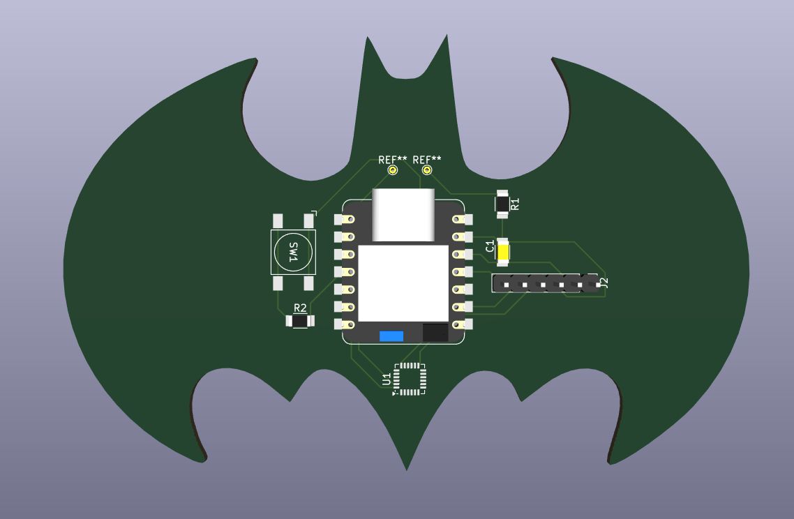
13. 3D Visualization: Open the 3D Viewer (Alt+3) to inspect the final result. This tool is essential for checking component clearances and the overall aesthetic of the board.
Simulation
1. Circuit Design for Simulation: I used KiCad's integrated SPICE simulator to test a Biased Diode Clipper circuit. This setup is designed to limit the voltage of an input signal at a specific threshold.
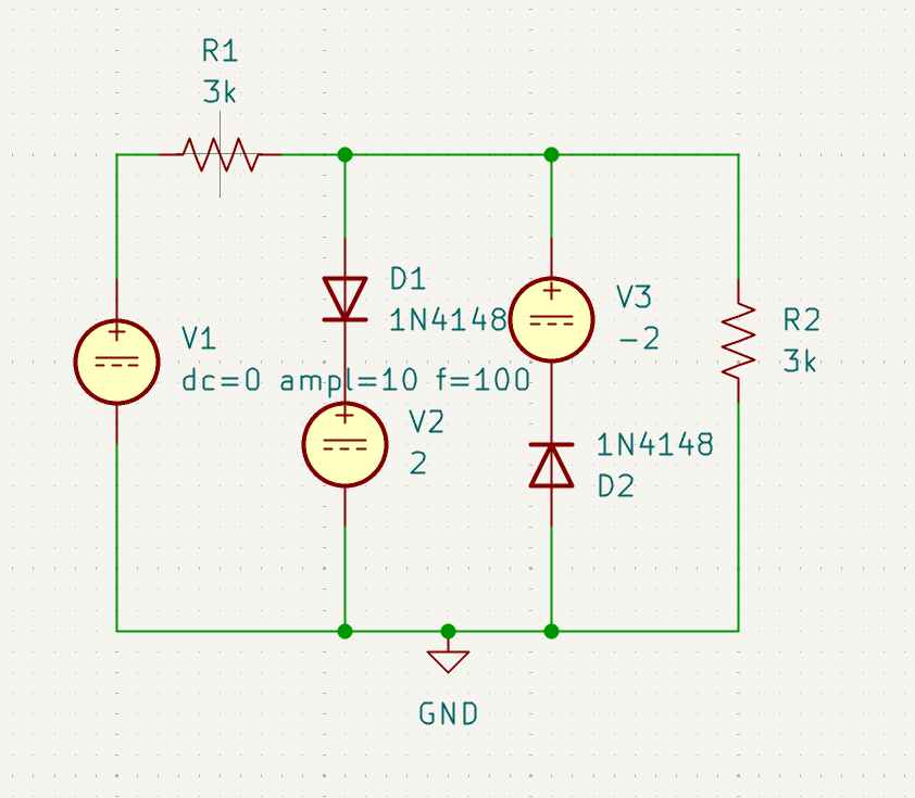
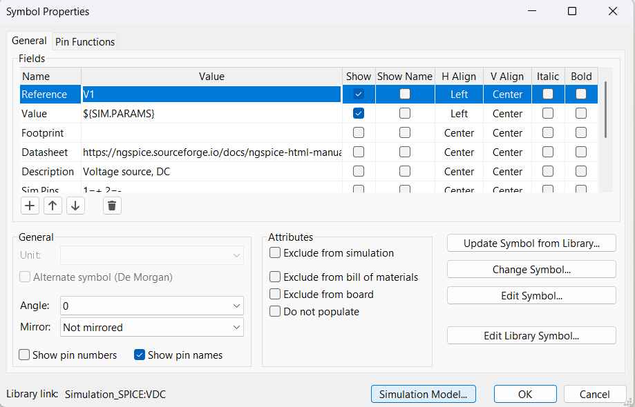
2. Component Configuration: To ensure accurate simulation results, right-click each component and enter Properties. It is vital that components have defined values for the simulator to calculate.
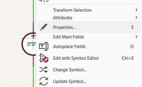
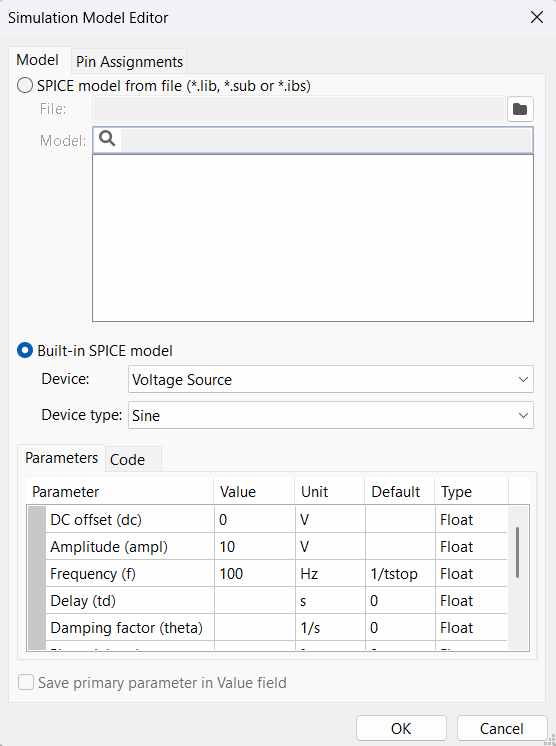
3. Simulation Models: Navigate to the Simulation Model tab. This is where you link the schematic symbol to a mathematical SPICE model that defines its electrical behavior.
4. Parameters Verification: Review the SPICE model parameters (such as diode saturation current or resistance values). These parameters dictate how the component will react under different electrical loads.
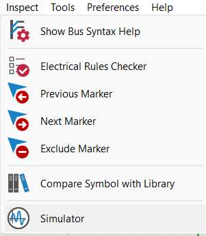
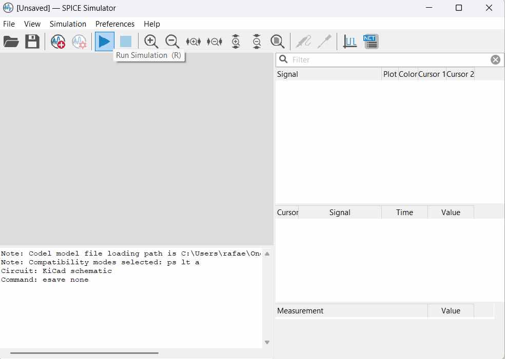
5. Launching the Simulator: Go to Inspect > Simulator. This opens the dedicated NGSPICE interface integrated into KiCad for real-time waveform analysis.
6. Initializing Simulation: Click the 'Run Simulation' button. At this stage, the software calculates the operating points of the circuit based on the defined input sources.
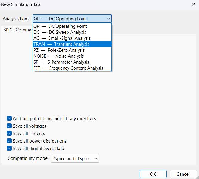
7. Transient Analysis: To observe the signal behavior over time (like an oscilloscope), change the analysis type to Transient Analysis. This is essential for visualizing AC waveforms and clipping effects.
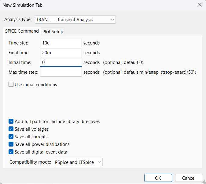
8. Time Constants: Define the Initial Time, Final Time, and Step Time. These settings determine the resolution of the graph; a smaller step time provides a smoother and more detailed curve.
9. Probing the Nets: Use the probe tool to select the specific Nets (Input and Output) you wish to visualize. Without selecting signals, the simulation window will remain blank.
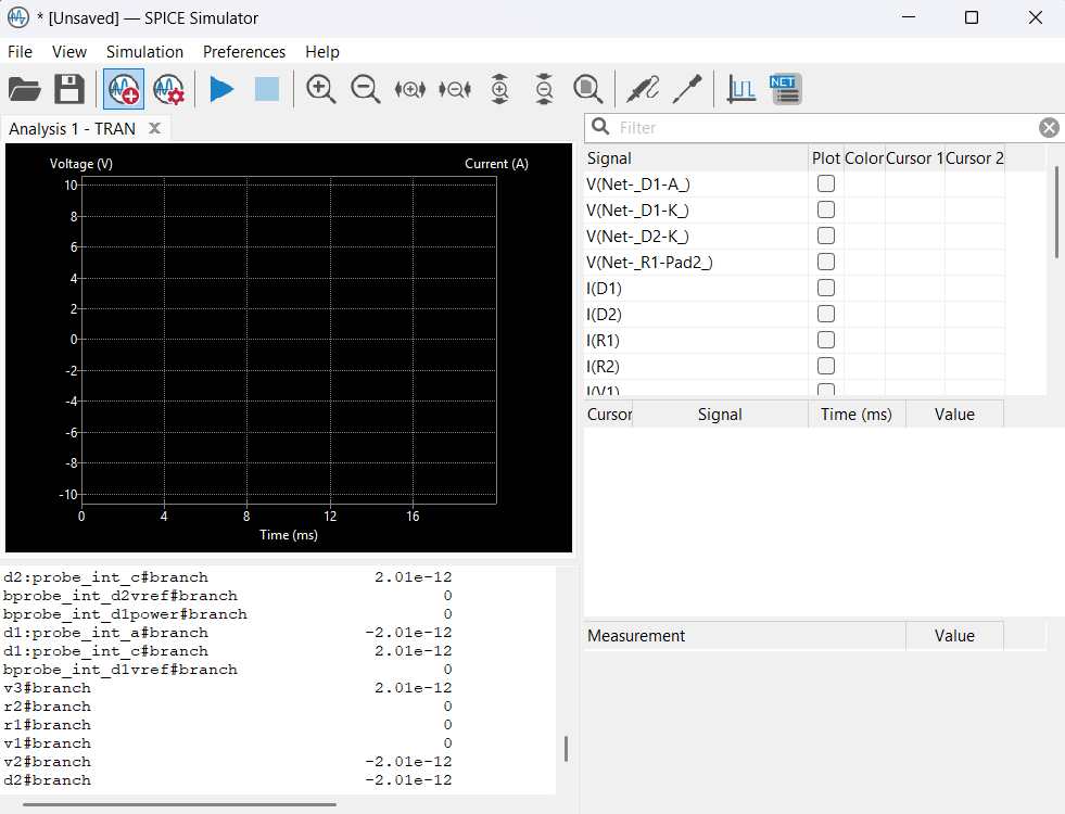
10. Signal Analysis: Finally, the simulation plot is generated. You can compare the input sine wave against the clipped output, verifying that the circuit behaves as intended according to the bias voltage.
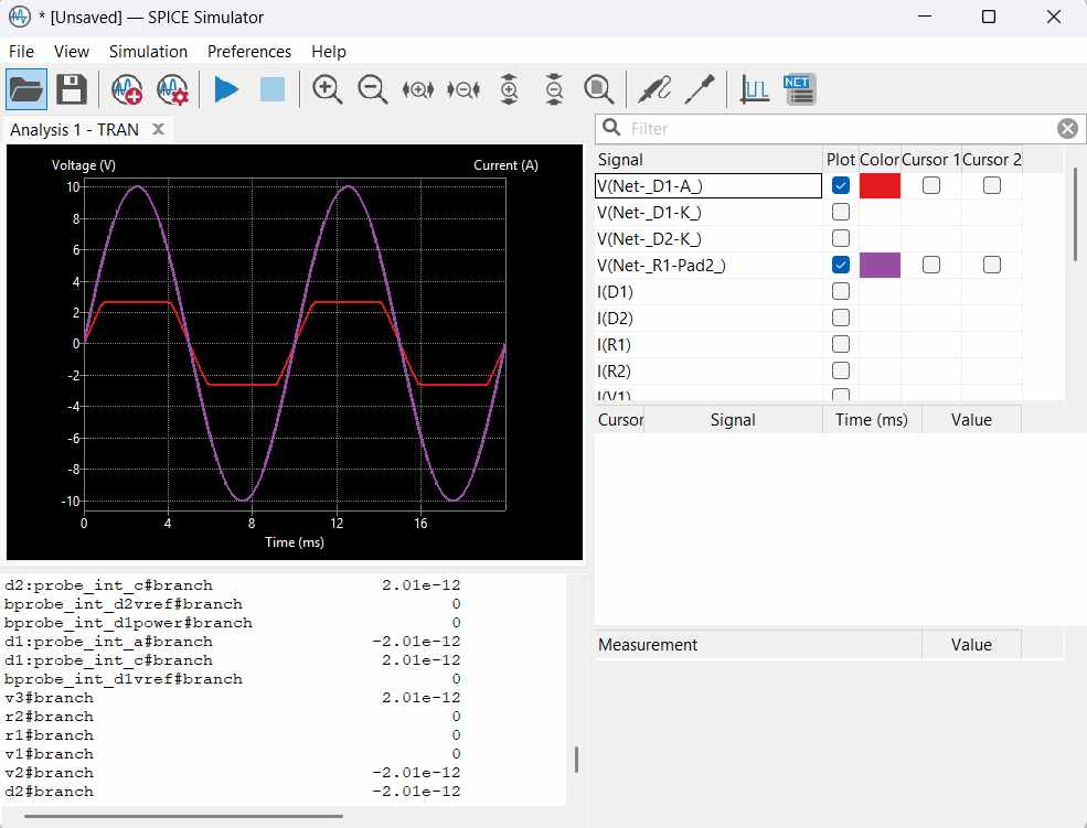
This week provided a comprehensive look at both the physical and theoretical aspects of electronics. Beyond the PCB layout, utilizing KiCad's integrated SPICE simulator for transient analysis was incredibly valuable for verifying circuit behavior before fabrication. Successfully simulating the biased diode clipper confirmed that my component values and power rails were correctly balanced. Combining these simulation results with a finalized 3D visualization ensures that the final manufactured board will meet both the electrical and mechanical requirements of my project.
Files
└── Week6PCB
    ├── dibujo.dxf
    ├── Week6.kicad_pcb
    └── Week6.kicad_sch
└── Simulation
    ├── Simulation.kicad_pcb
    ├── Simulation.kicad_prl
    ├── Simulation.kicad_pro
    ├── Simulation.kicad_sch
    ├── Simulation.wbk
    └── Simulation-backups
        ├── Simulation-2026-03-03_215808.zip
        └── Simulation-2026-03-03_224540.zip