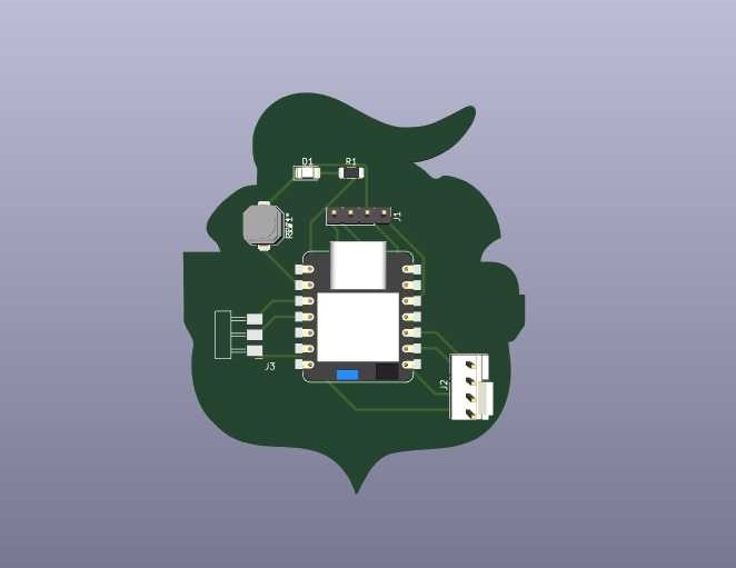
Making a pcb board with the Club Puebla shield as a design.
00. MISSION BRIEFING
For this week's objective: create a pcb board that integrates LEDs and a push button, all controlled by a XIAO RP2040/RP2350.
TEAM PROTOCOL (GROUP ASSIGNMENT)
As part of our mission, we had to characterize the design rules for our in-house PCB production process (feeds, speeds, tool sizes, etc.). You can read all the intel and documentation gathered by our team by clicking below:
To complete this mission, I gathered the following components from the Fab Lab inventory:
Seeed Studio XIAO RP2040/RP2350 (The Brain)
Push button With a pull-up resistor
LEDs 1206 SMD (Visual feedback)
Resistors 1206 SMD (Current limiting for the LEDs)
Pin Headers (For connections)
02. THE BLUEPRINT (KICAD DESIGN & EXPORT)
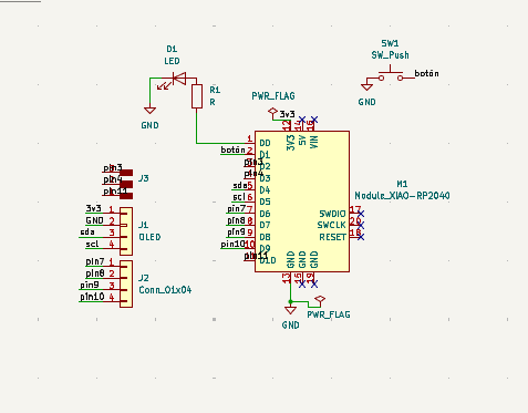
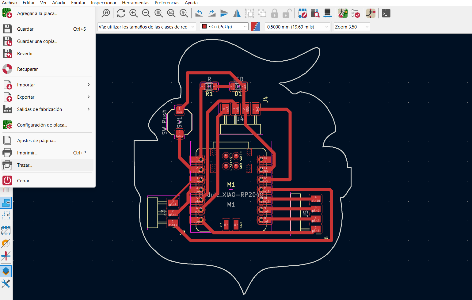
To kick off the blueprinting phase, I recycled the exact same schematic design from Week 06. Since the logic was already perfectly established and verified, I just forged ahead into the PCB editor, routing the traces with a safer 0.8mm width.
1 / 2
01. Repurposing the mission schematic from Week 06 for the sound protocol.
02. Routing the copper traces with a safer 0.8mm width.
THE WORKFLOW: GERBER TO PNG
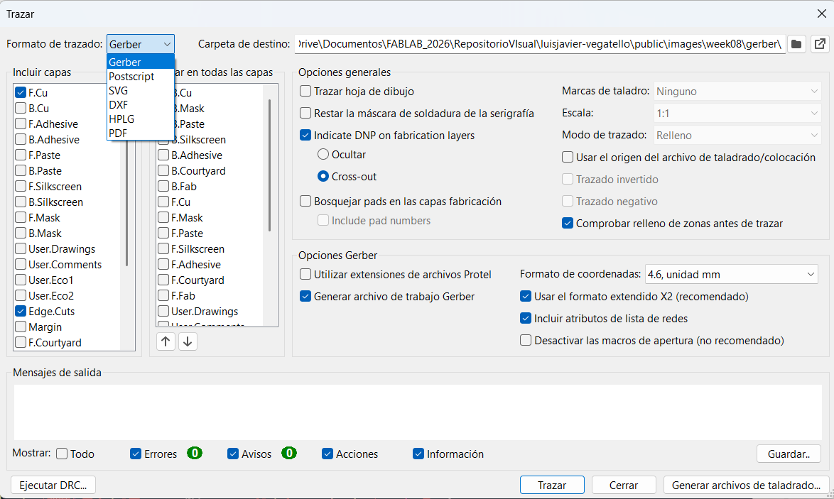
The Roland SRM-20 cannot read raw vector lines natively through Mods. It requires high-contrast raster images to calculate the 3D toolpaths. To achieve this, I exported the F.Cu (Front Copper) and Edge.Cuts layers as Gerber files.
Then, I used the gerber2png.fablabkerala.in tool to convert these mathematical vector files into high-resolution (1000 DPI) monochrome PNGs.
Why PNGs? In these images, white represents the material that must remain (the copper traces and pads), while black represents the areas where the endmill will remove material to isolate the circuits. For the outline, the white shape tells the machine the exact boundaries of the board to cut out.
1 / 2
01. Setting up the Plot window to export F.Cu and Edge.Cuts as Gerber files.
02. Converting the mathematical Gerber data into high-contrast PNG images via Kerala tool.
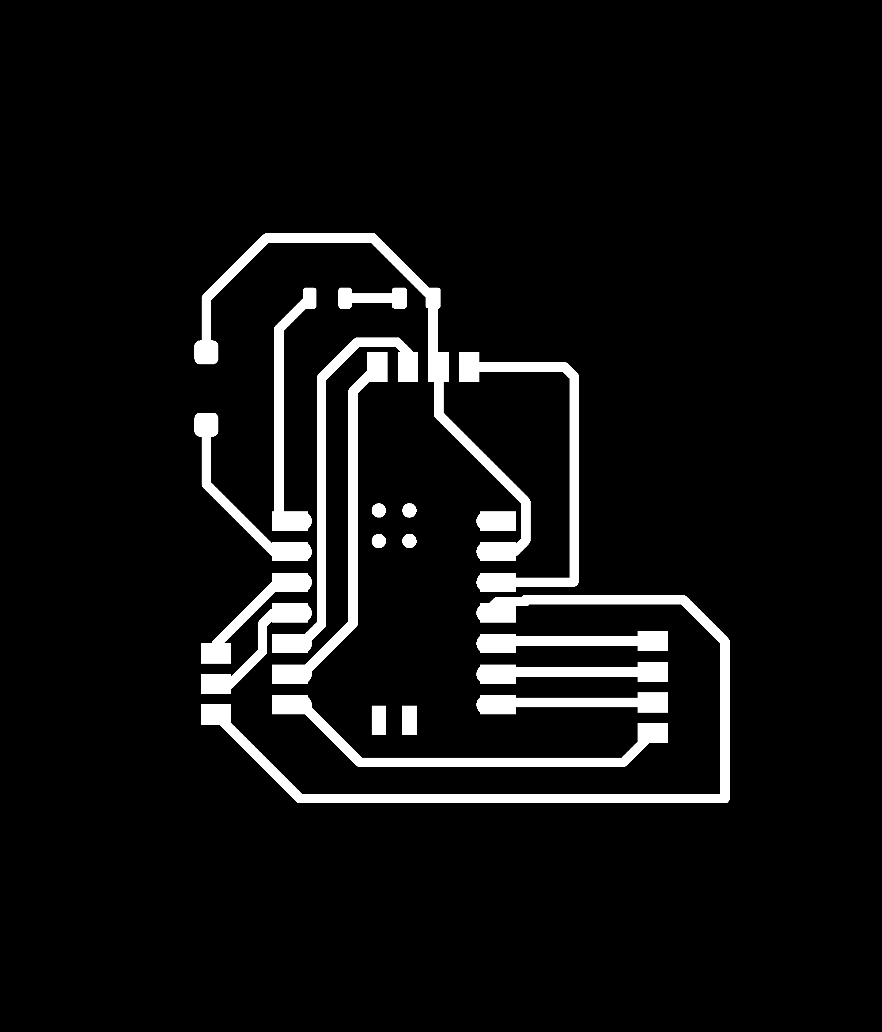
THE FINAL PNG FILES
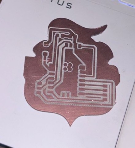
Here are the actual high-contrast PNG files generated by the tool, ready to be processed by Mods. Notice the strict black and white contrast required by the milling machine.
01. Traces (F.Cu) - White paths will be kept as copper.
02. Outline (Edge.Cuts) - White shape defines the cut limit.
03. GENERATING TOOLPATHS (MODS)
With the high-contrast PNGs ready, I imported them into Mods CE. Mods analyzes the pixels and calculates the exact G-code (in this case, an `.rml` file) that tells the Roland machine where to move on the X, Y, and Z axes.
⚙️ MODS CONFIGURATION & TOOL SELECTION
It is critical to configure the right parameters for each operation depending on the physical endmill used:
OPERATION
TOOL SIZE
CUT DEPTH
OFFSETS & SPEED
Traces (Isolating Copper)
1/64 inch (0.4mm)
0.004 in
Offset: 4 | Speed: 3 mm/s
Outline (Cutting Board)
1/32 inch (0.8mm)
0.024 in (Max: 0.072)
Offset: 1 | Speed: 3 mm/s
Why 1/64" for traces? Because it's fine enough to pass between the tiny legs of the XIAO RP2040 without destroying the pads. We use 4 offsets to clear enough copper around the traces to make soldering easier and prevent short circuits.
Why 1/32" for the outline? It's a thicker, stronger tool capable of cutting all the way through the tough FR1 material without breaking.
Full screencast of the Mods toolpath generation protocol.
04. MACHINE SETUP & PHYSICAL CALIBRATION
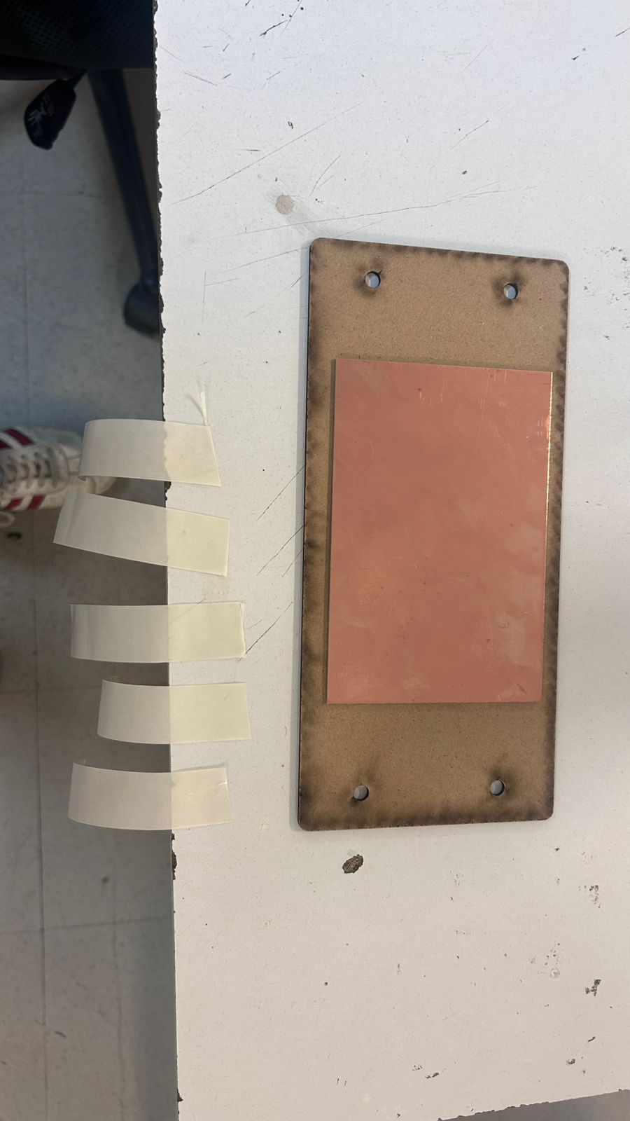
Before hitting "Cut", physical preparation is mandatory. I secured the FR1 copper board to the sacrificial layer using strong double-sided tape. Then, I installed the 1/64 endmill.
Setting the Z-Axis: This is the most delicate part. I lowered the spindle via VPanel until the endmill was a few millimeters above the copper. Then, I loosened the setscrew, carefully let the tool drop to touch the board surface, pressed it gently down, and tightened the screw. This establishes a perfect Z=0 physical origin.
01. Securing the board with double-sided tape.
Calibrating the Z-Axis.
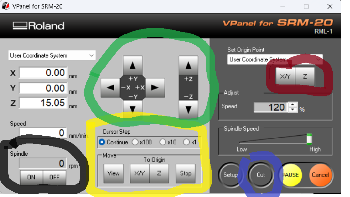
VPANEL INTERFACE
Inside the VPanel software, I set the X/Y origin where I wanted the cut to start, and registered the Z origin based on the physical calibration described above. I have marked the exact buttons used for this process below.
1 / 2
01. VPanel interface highlighting the essential machine controls.
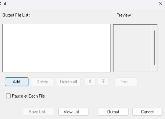
02. Loading the .rml toolpath file into the spooler.
🕹️ VPANEL COLOR LEGEND
🟢 Green: Used to manually move the tool along the X, Y, and Z axes.
🟡 Yellow: Used to quickly move the machine back to the previously saved origin point.
🔴 Red: Used to set and save the current position as the new X/Y or Z origin.
🔵 Blue: Used to open the spooler, import the `.rml` files, and start the cutting process.
⚫ Black: Used to manually turn the spindle on or off (useful to verify rotation or warm up).
05. THE MILLING ACTION
With all parameters verified and the enclosure closed, the MonoFab SRM-20 went to work. Here is the physical fabrication process captured on video.
1 / 3
01. Changing and calibrating the endmill tool.
02. Milling the intricate copper traces (1/64").
03. Cutting the final PCB outline border (1/32").
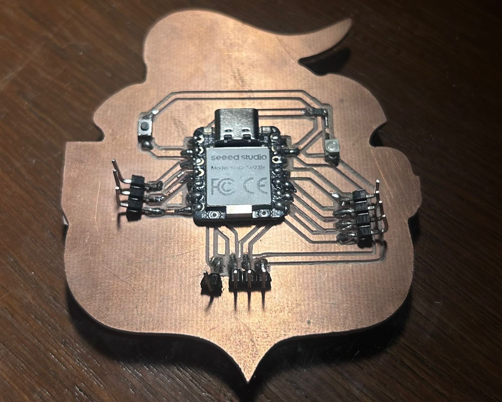
06. BOARD POPULATION (SOLDERING PROTOCOL)
The dust settled, and the board emerged perfectly isolated. The next step was washing it and populating it with the electronic components.
🔥 SOLDERING SPECIFICATIONS
Temperature: The soldering iron was set between 350°C and 380°C to ensure a quick melt without burning the FR1 substrate or the tiny SMD components.
Material: I used standard Sn60/Pb40 Rosin Core solder.
Technique: Flux was generously applied to the pads. I used tweezers to hold the 1206 SMD LEDs and resistors, tacking down one pad first to anchor the component before soldering the other side.
01. The unpopulated, freshly milled PCB ready for the soldering iron.
02. Soldering Process in action. Tacking down pads with flux.
07. FINAL HERO SHOT & SYSTEM TEST
After careful soldering and cleaning, the board was fully assembled. Here is the macro shot showing the quality of the solder joints, followed by the physical test to verify the integrity of the circuit and the logic.
Displaying the final populated board and solder joints.
Hero Test: Interacting with the push button. System fully operational.
08. PROGRAMMING & LOGIC (ARDUINO IDE)
With the hardware assembled, it was time to give it a brain. I used the Arduino IDE to program the microcontroller.
The Logic: The code is straightforward but effective. I defined the input for the push button on GPIO 27 (using the internal pull-up logic to ensure a stable reading) and the output for the red SMD LED on GPIO 26. The loop() continuously monitors the button's state. When pressed, the circuit closes to ground (reading LOW), which triggers the microcontroller to send a HIGH signal to the LED, turning it on.
// CLUB PUEBLA LED PROTOCOL (.ino)
const int ledPin = 26;    // SMD Red LED connected to GPIO 26
const int buttonPin = 27; // Push button connected to GPIO 27

void setup() {
  // Initialize the LED pin as an output:
  pinMode(ledPin, OUTPUT);
  // Initialize the pushbutton pin as an input with internal pull-up:
  pinMode(buttonPin, INPUT_PULLUP);
}

void loop() {
  // Read the state of the pushbutton value:
  int buttonState = digitalRead(buttonPin);

  // Check if the pushbutton is pressed.
  // With a pull-up resistor, the button reads LOW when pressed.
  if (buttonState == LOW) {
    // Turn LED on:
    digitalWrite(ledPin, HIGH);
  } else {
    // Turn LED off:
    digitalWrite(ledPin, LOW);
  }
}