6. Electronics design
Group AssignementThis week I learned how to design circuits on my own. Taking what we learned in Week 4. Embeded programming, I analized the components and connections to transfer them into a Schematic and then a PCB.
In the beginning I wanted to copy the simulation identically (with an ESP32 WiFi), but I realized this microcontroler was too much for the simple circuit I actually had. So I decided to downgrade to a generic XIAO module. (Also to simplify my work a little while I learn)
I had to look at the datasheets of different XIAO controlers and all my components to make sure I made the right connections.
KiCAD is the software I used for this week's assignement. It is an amazing open source suite with embedded systems that allow you to design from the schematic, to the PCB, simulations and even 3D designs of the circuit.
Walk through my process:
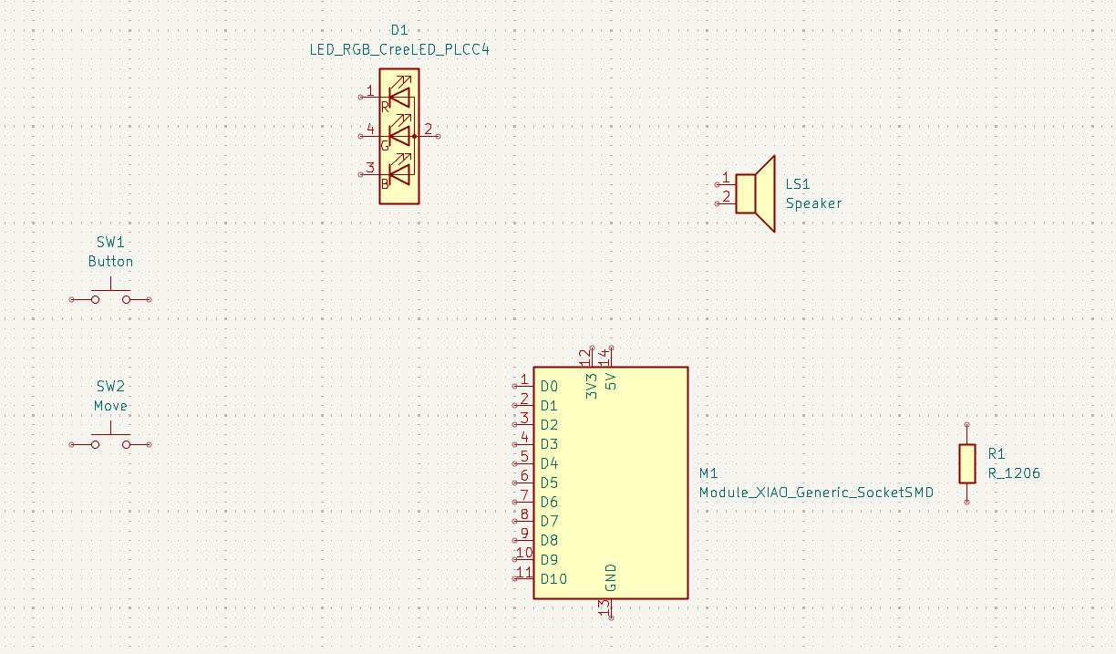
Selecting and placing my components from the FabLib Library.
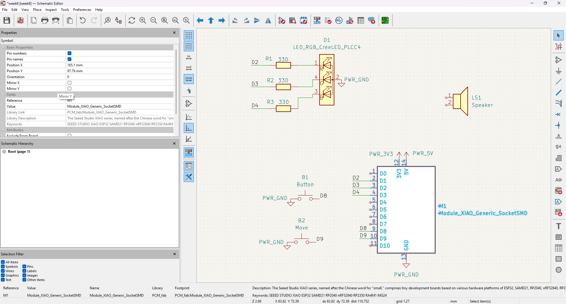
Connecting all components between them and adding Power lines: voltage (5V and 3V) and Ground.
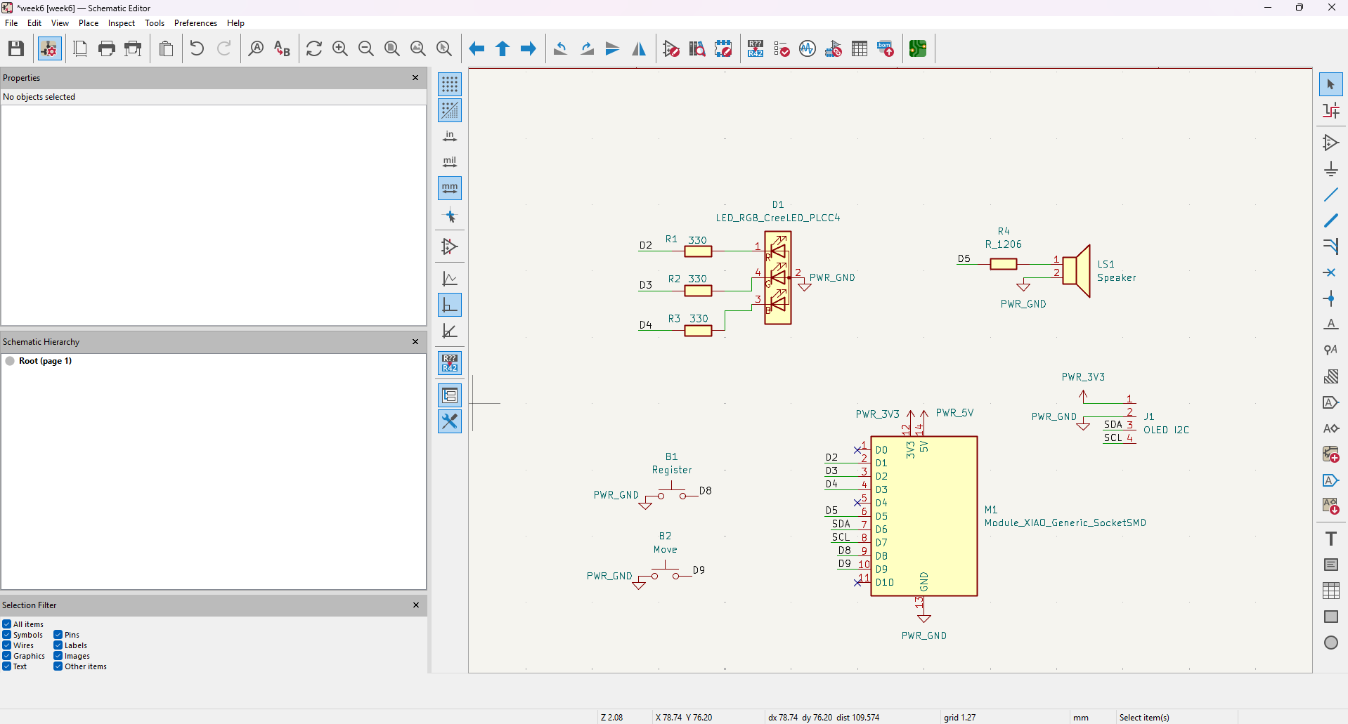
Adding some pins for an OLED display.
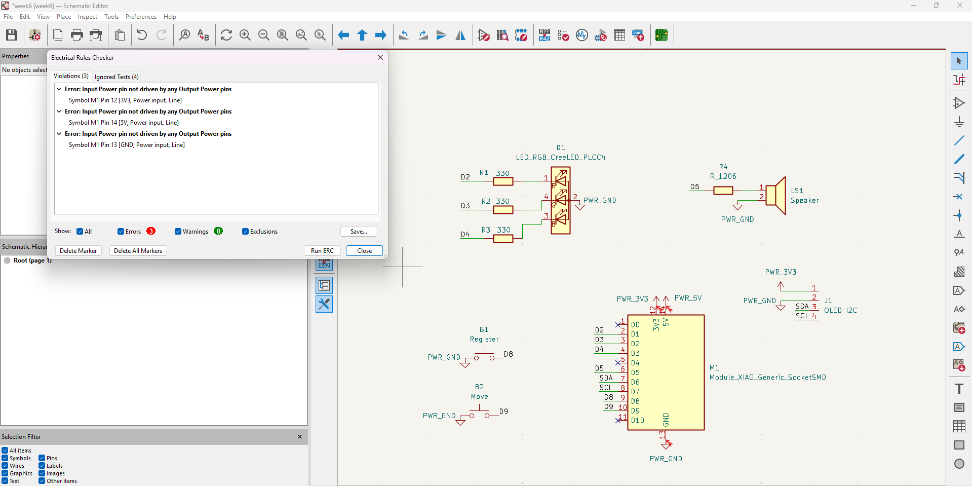
Doing Electrical Rules Checking and finding out all power inputs had to be better defined.
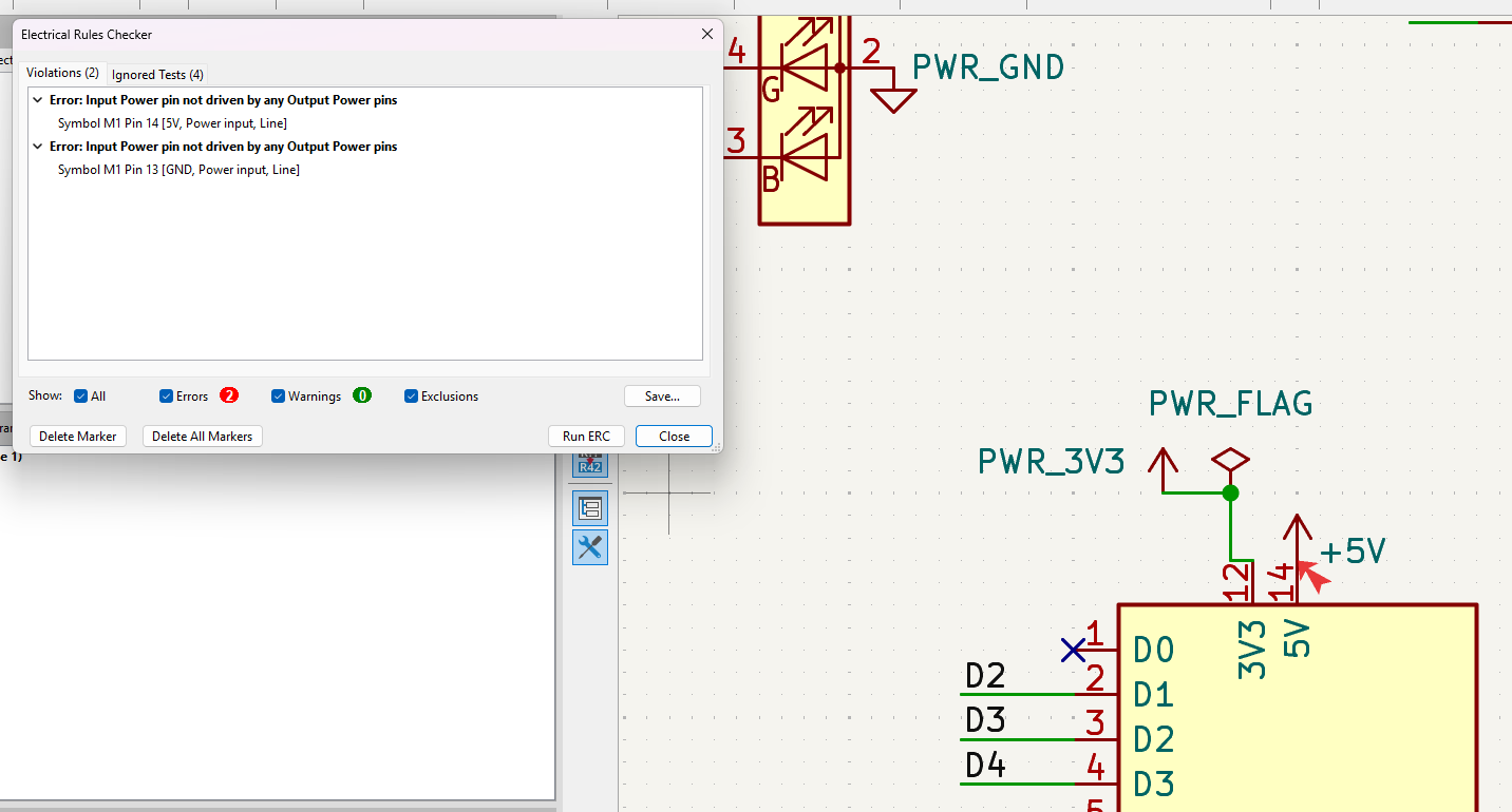
I tried two different ways and found the right one.
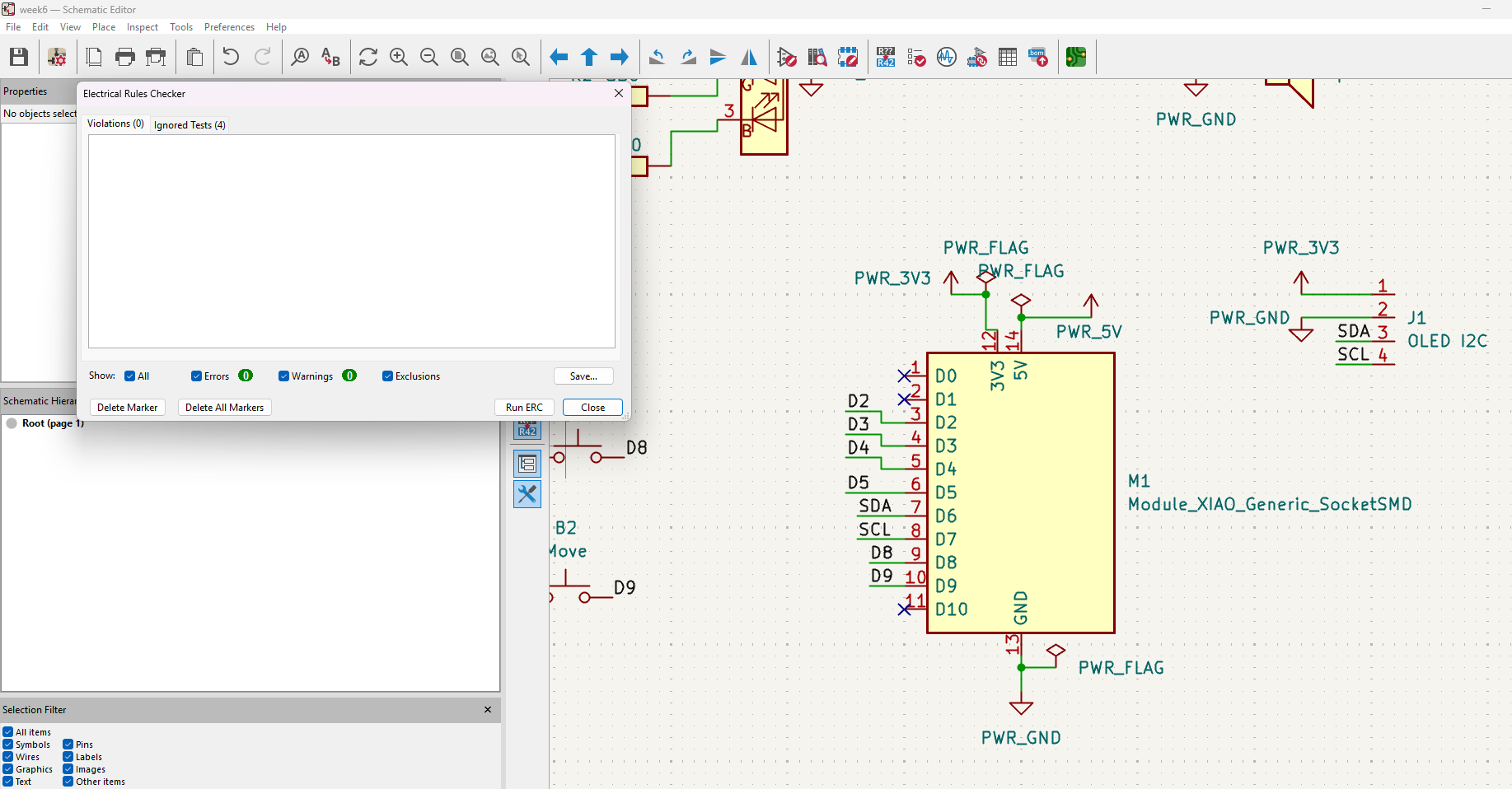
Finally got my schematic right.
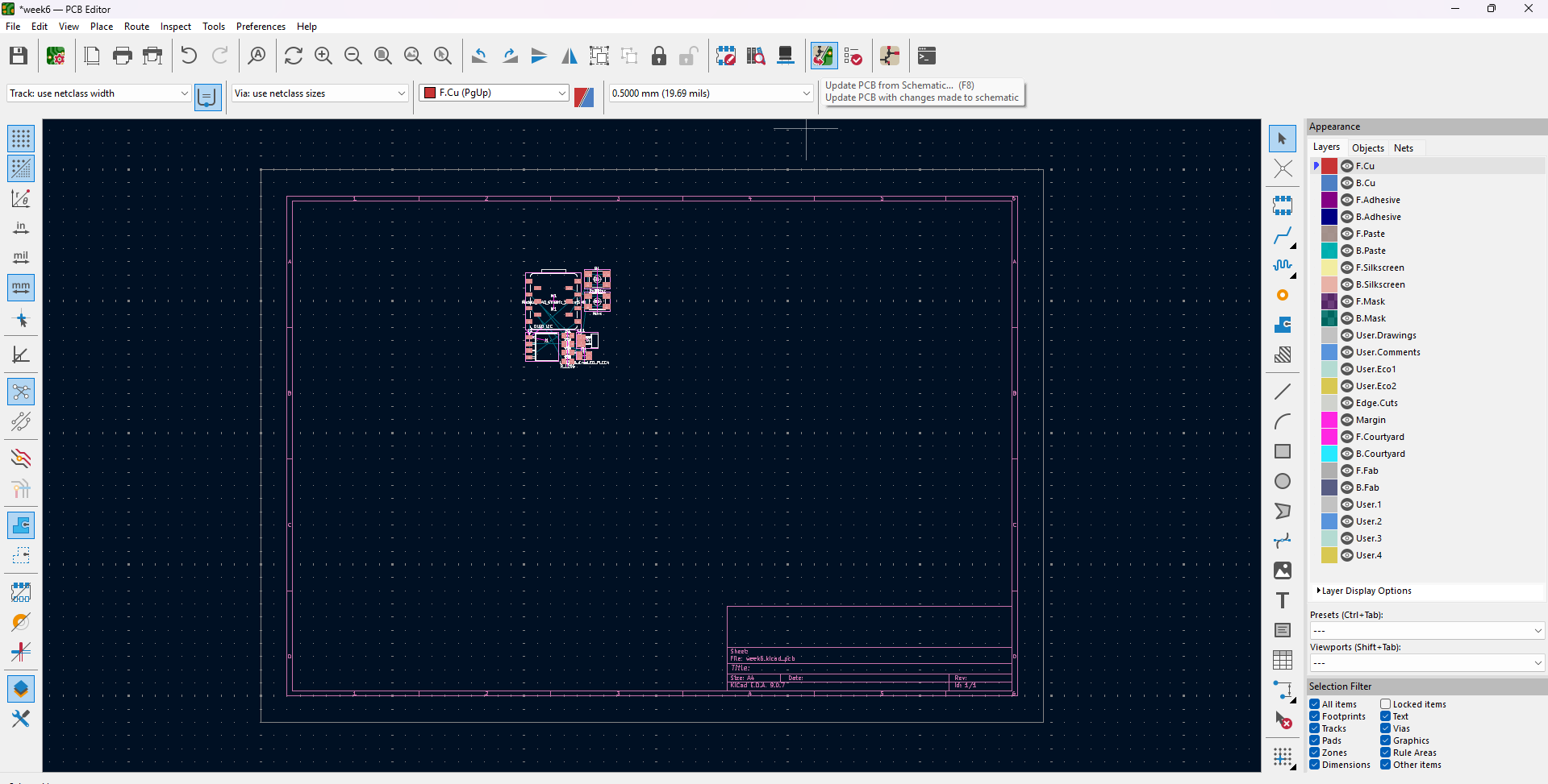
Imported components from the schematic.
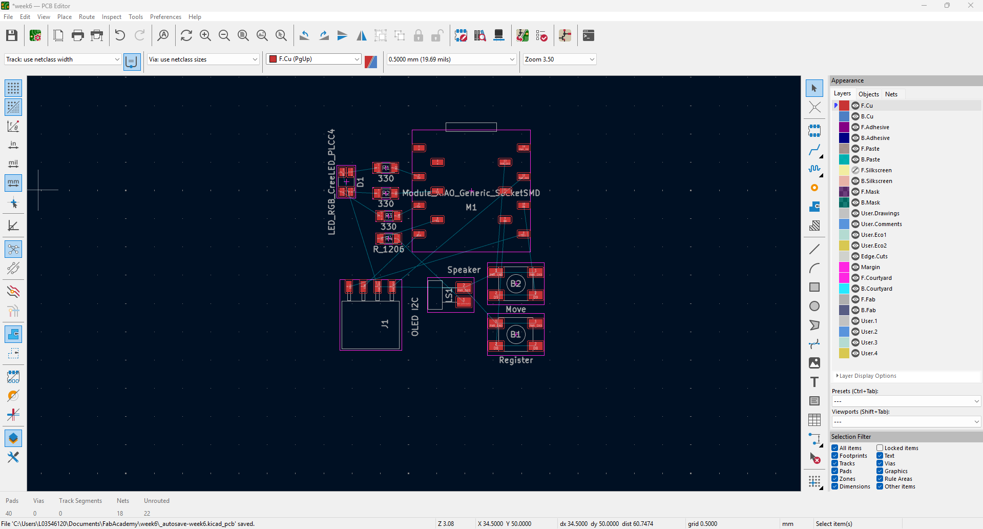
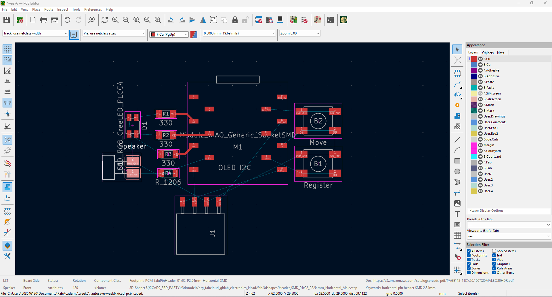
Started placing the components where I saw best for the connections.
Started drawing paths manually, while thinking there should be an automated way to do this. So I looked for a "freerouting" pluginn and installed it.
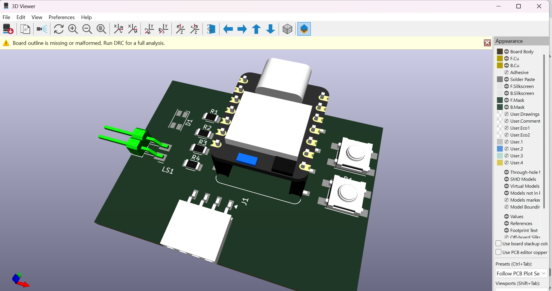
Checked my first 3D model to see how the would look.
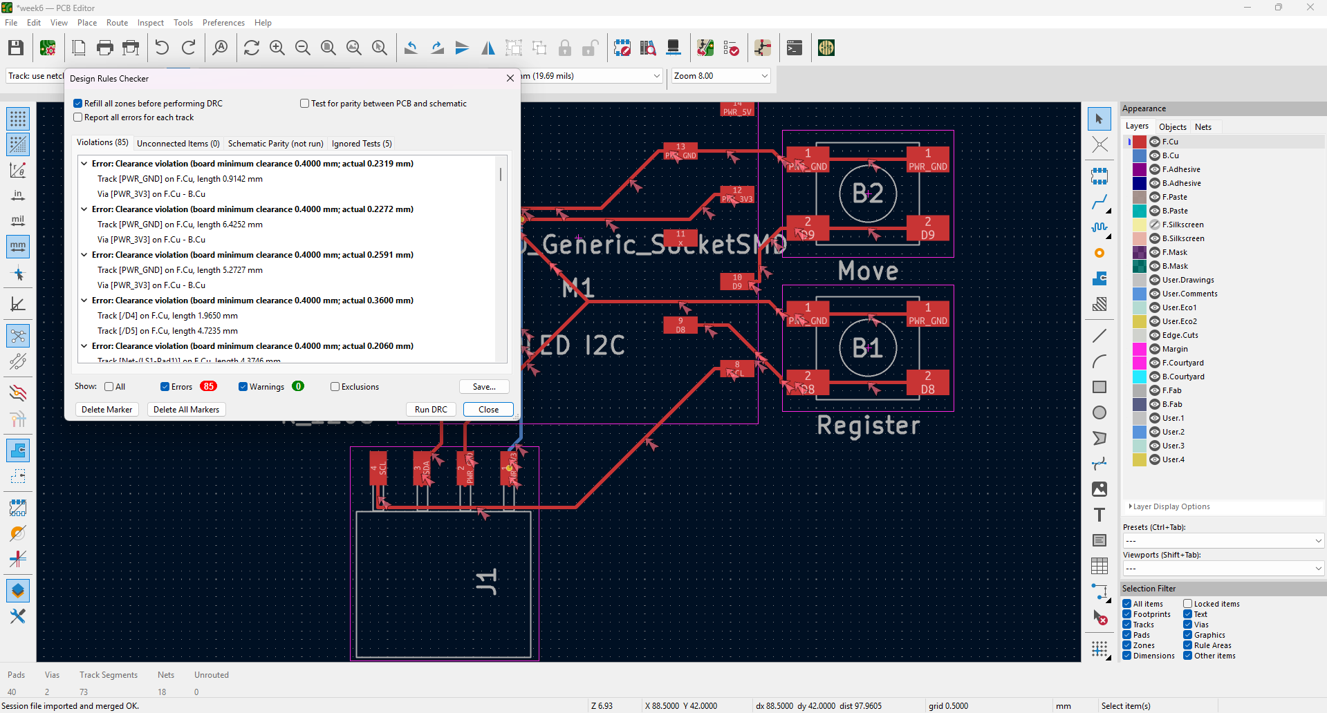
A bunch of errors showed up from that automated "freerouting". I freaked out and aborted this option. (Erasing al tracks that where created)
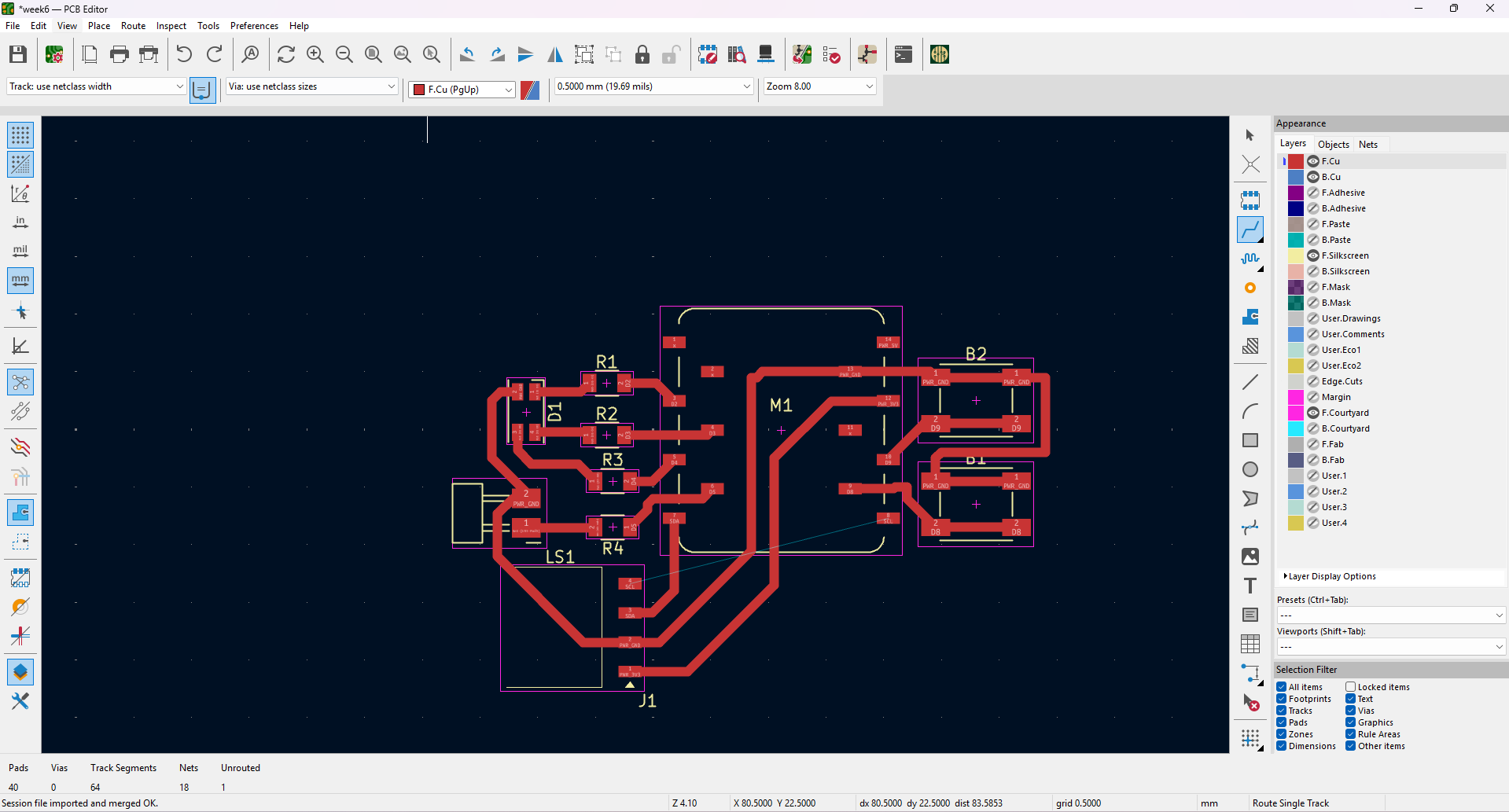
Manually drawing tracks and placing components to avoid crossing paths.
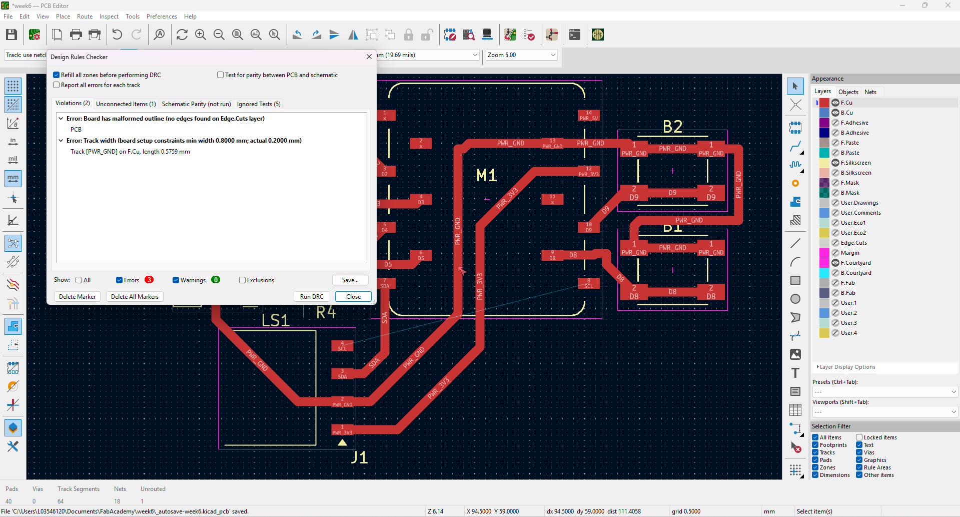
Identifying and correcting design errors.
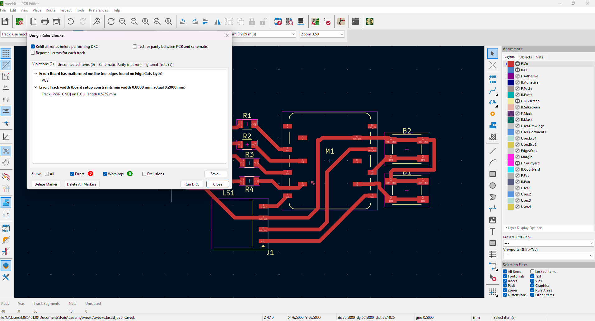
Identifying and correcting design errors... again. I had to go back to the schematic and make some adjustments. Luckily it is pretty easy to do on KiCad and syncronization is great.
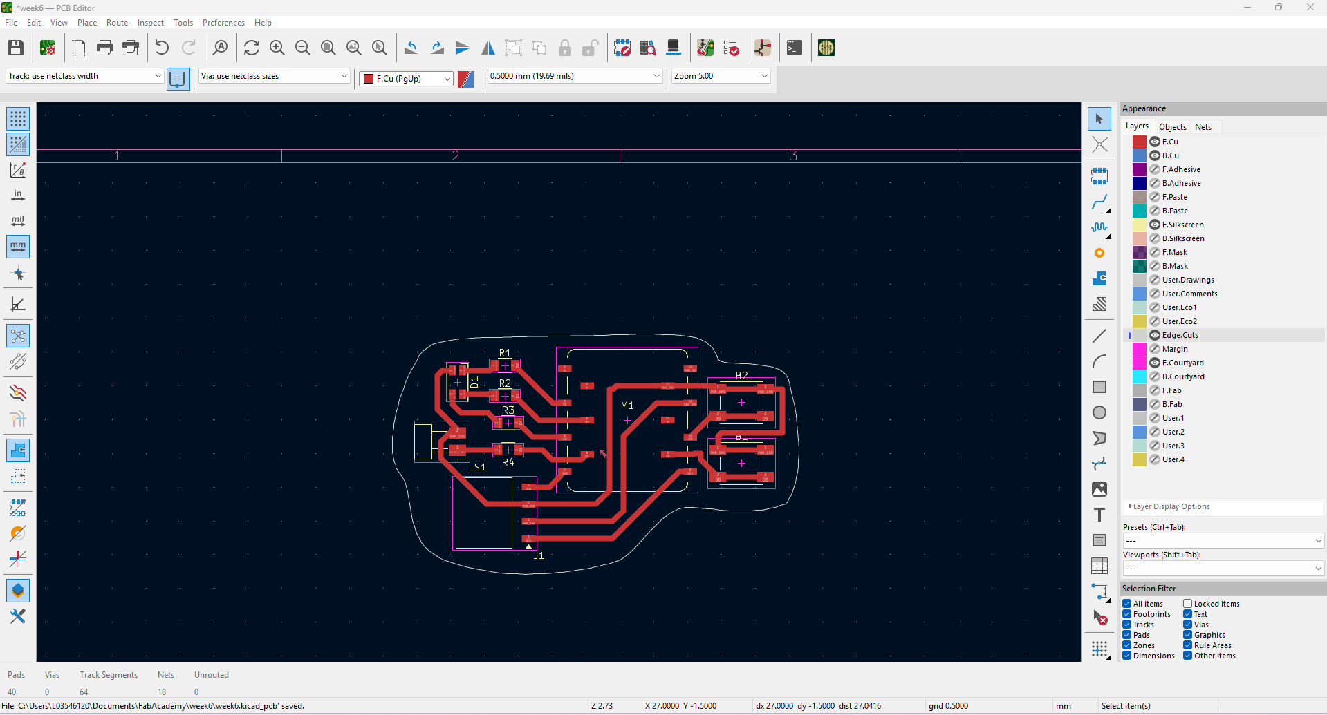
Sketching the Edge Cuts.
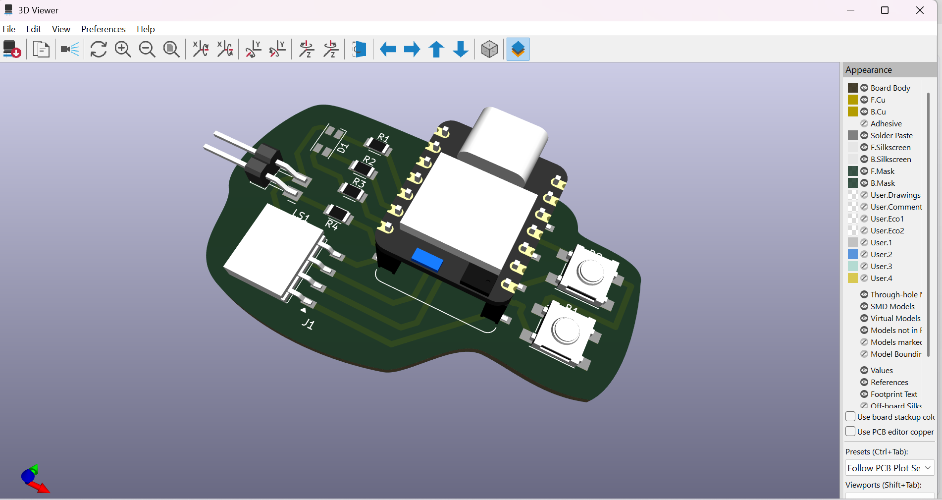
A 3D view of what the final circuit would look like.
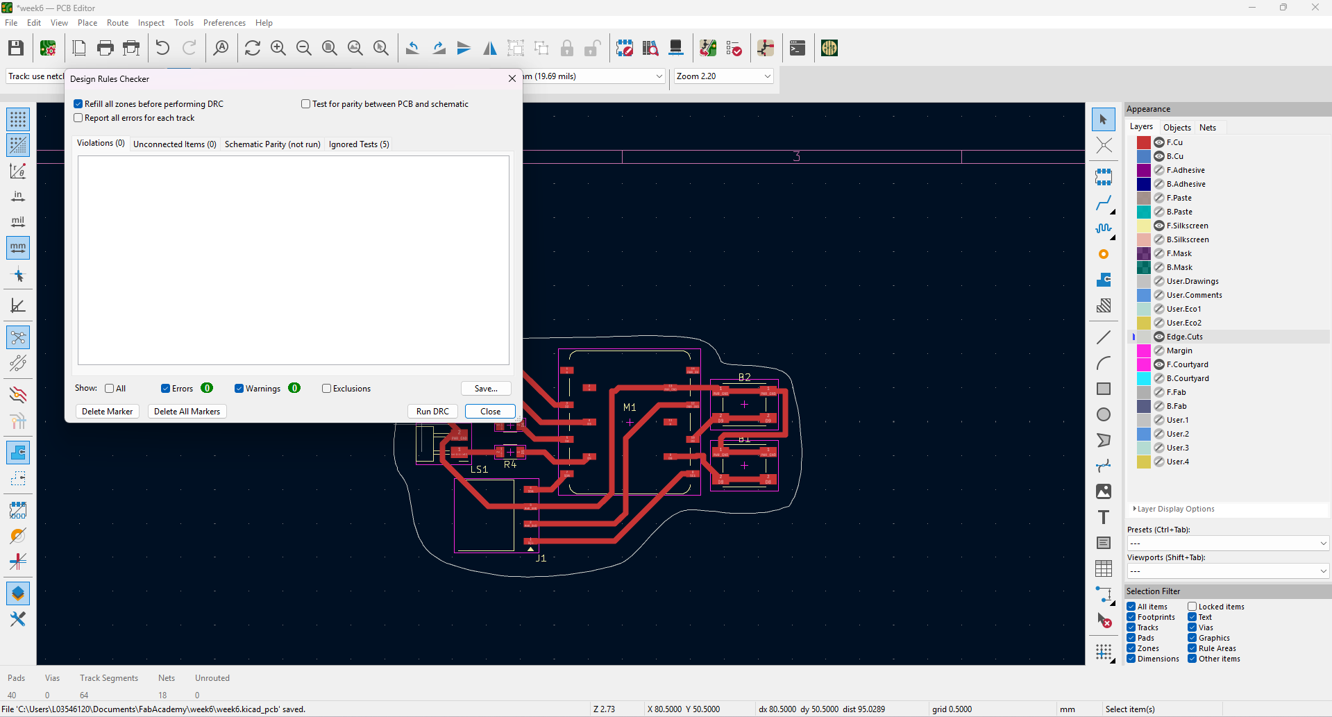
Fianlly, got the Design Rules Checker to 0.
Some of of my learnings:
- FabLib is an amazing library of components curated by the FabLab team. It includes all components expected to be available in any FabLab. (Both schematic and PCB footprint)
- It is important to use the Ohm Law (V=RI) to check for the right resistance and, current and voltage according to the present components.
- Taking into account the milling tool for the design is very important, otherwise the paths or positioning between components might crash or missfit.
- Temperature is also important to consider. As current is flowing through the ciruit, it is innevitable that the temperature rises. KiCad has a cool calculator that helps to check ideal track-width.(The track width should not be wider than the components' mounting areas)
- Indicating unused pins is as important as connecting components.
- There are so many components, sizes, colors and variations which is why it is VERY important to learn how to read datasheets.