Week 7: Computer Controlled Machining
Group assignment
Week 7CNC Router
CNC stands for Computer Numerical Control. It refers to machines that are controlled by code to automate tasks like cutting, drilling, and shaping as part of a digital manufacturing process. A CNC machine is essentially a computer that takes code and turns it into motion.
Types
Milling machines: Versatile CNC machine tools that carve 2D and 3D shapes out of metal, plastic, or wood, including milling in 3-, 4-, and 5-axis configurations for more complex geometry and fewer setups.
Additing manufacturing machines: Additive manufacturing (AM) machines, or 3D printers, create 3D objects from digital files by depositing materials in layers. For more datails you can go to my Week 5.
Laser Cutting Machines: Are Computer Numerical Control (CNC) tools that use a high-powered, focused laser beam to cut, engrave, or mark materials with high precision and speed. For more datails you can go to my Week 3.
CNCs use to types of code, G-CODE and M-CODE:
G-CODE is a programming language for CNC that instructs machines where and how to move. The G in G-CODE stands for "Geometric" because is the type of movement the code produces.
G-CODEN## G## X## Y## Z## F## S## T## M## N##: Line Number.G##: Motion.X##: Horizontal Position (X axis).Y##: Vertical Position (Y axis).Z##: Depth (Z axis).F##: Feed Rate.S##: Spindle Speed.T##: Tool selection.M##: Miscellaneous functions.M-CODE is a programming language for CNC that instructs machines on what to do. The M-CODE has miscellaneous functions, bit it doesn't instructs on where to go.
Miscellaneous functionsM00:Program stop. M01:Optional program stop. M02:End or program. M03:Spindle on clockwise. M04:Spindle on counterclockwise. M05:Spindle stop. M06:Tool change. M07:Flood coolant on. M08:Flood coolant off. M30:End of program / Return to start. M41:Spindle low gear range. M42:Spindle high gear range.
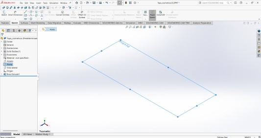
Design
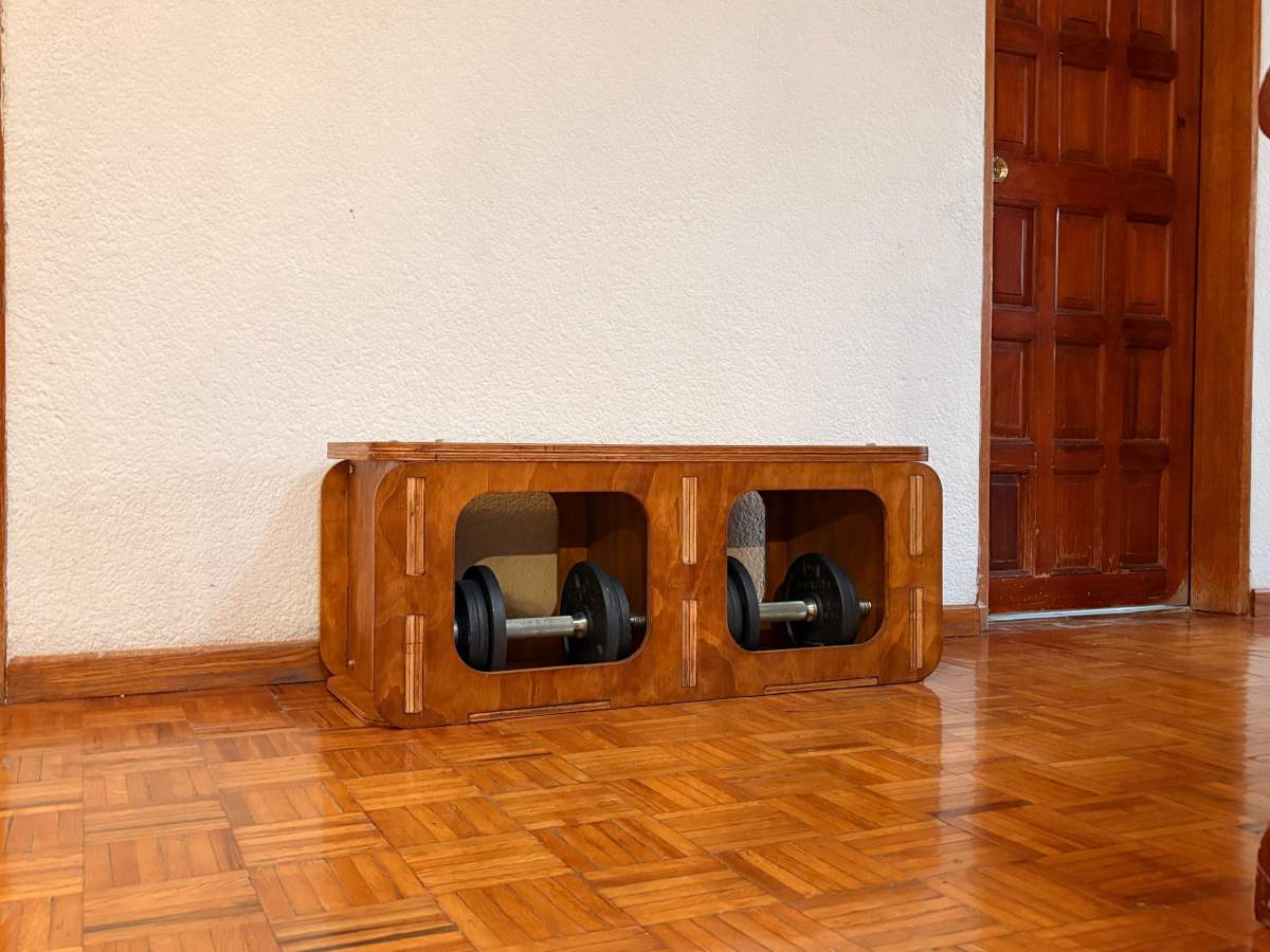
My plan is to design and build a multifunctional piece of furniture that combines several purposes into a single compact structure. The main idea is for it to work as a bench press station for workouts, while also providing organized storage space for my dumbbells and other gym accessories. In addition, I want it to function as a small bench that can be placed in my living room and blend naturally with the rest of the furniture. One of the most important aspects of the project is achieving a minimalist design. I want the structure to look clean, modern, and simple, without unnecessary elements that make it appear bulky or complicated.
Base
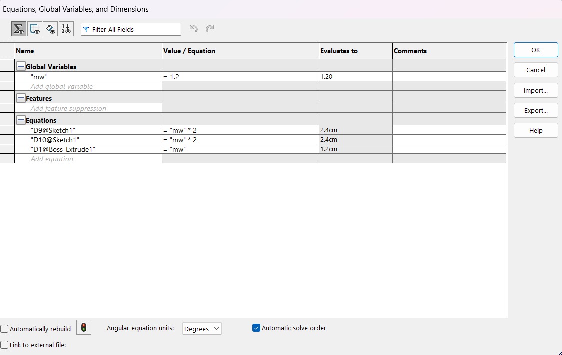
Equation.
mw (material width).1.2 cm.
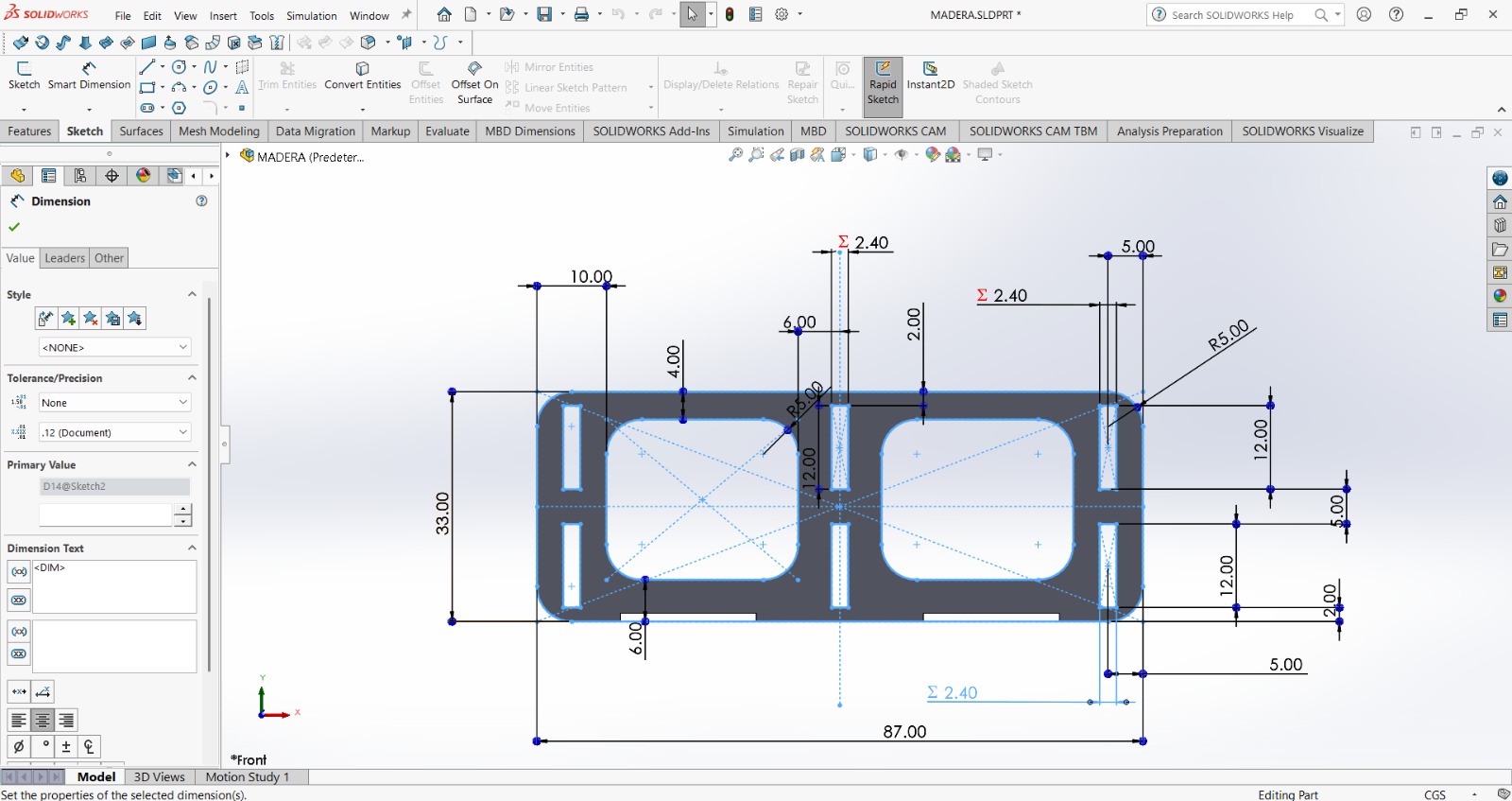
Base
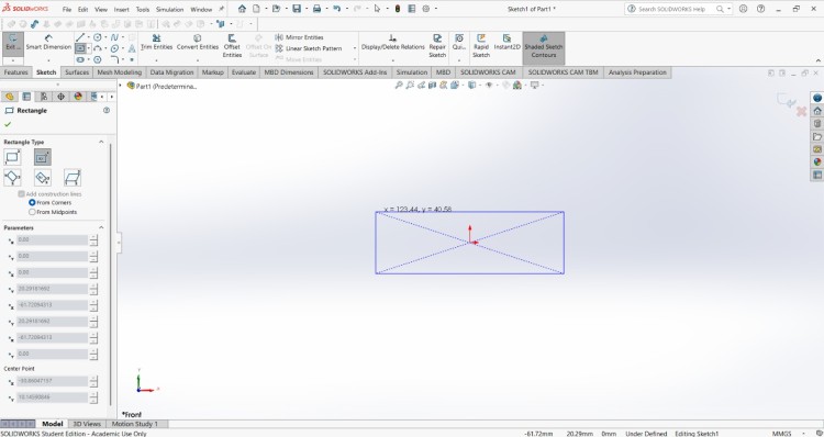
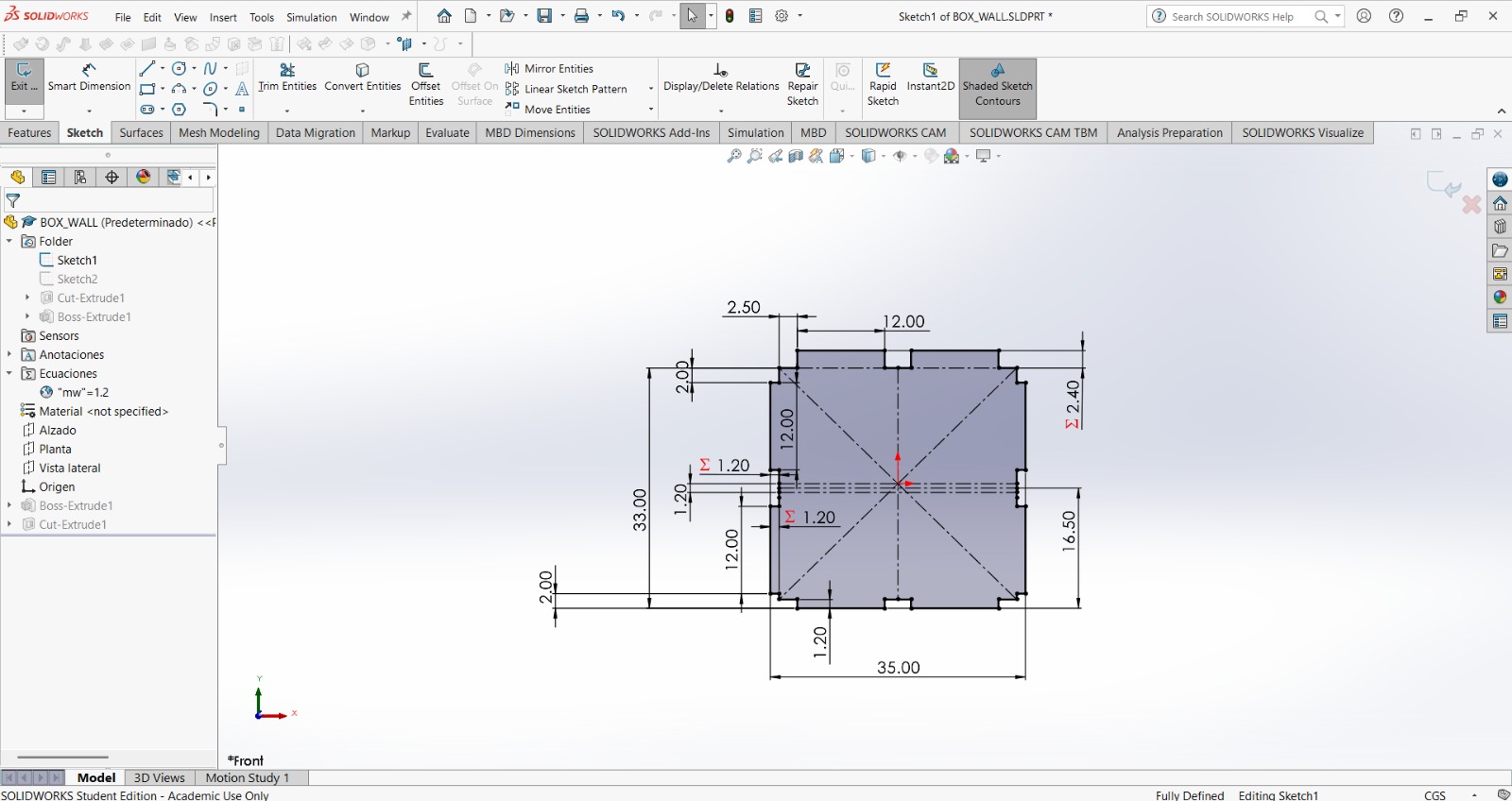
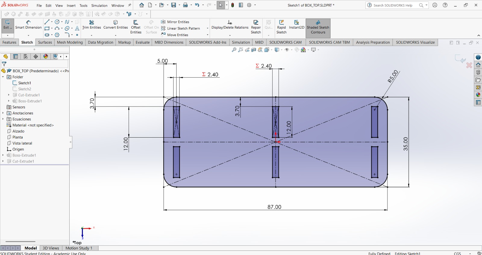
1. First, I changed the document units to CGS and created a center point rectange of 87X35 cmin the top plane.
Base
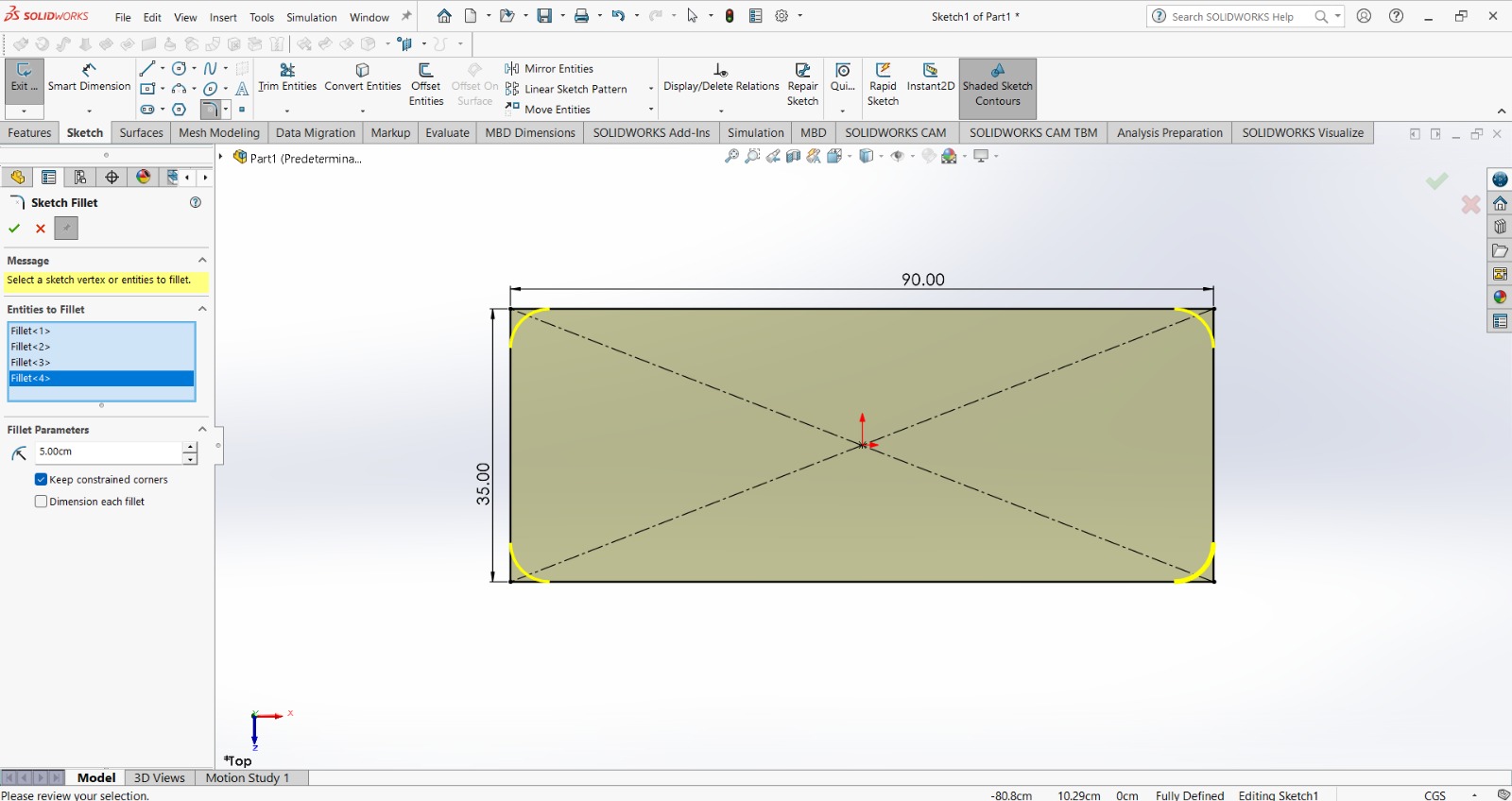
2. Then, using the sketch fillet in all the corners I made arcs of 5 cm.
Base
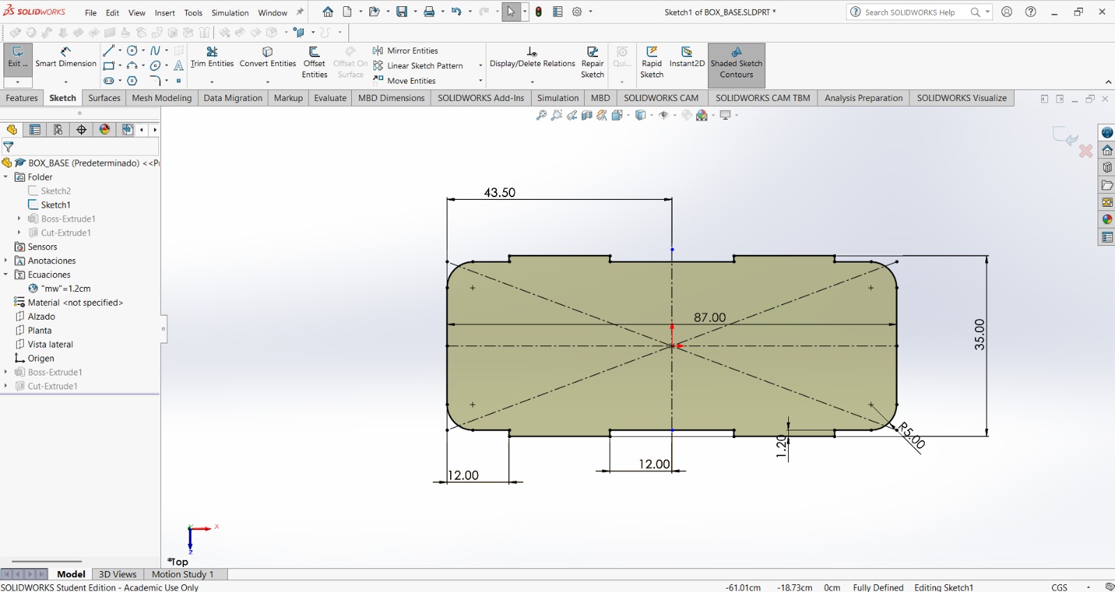
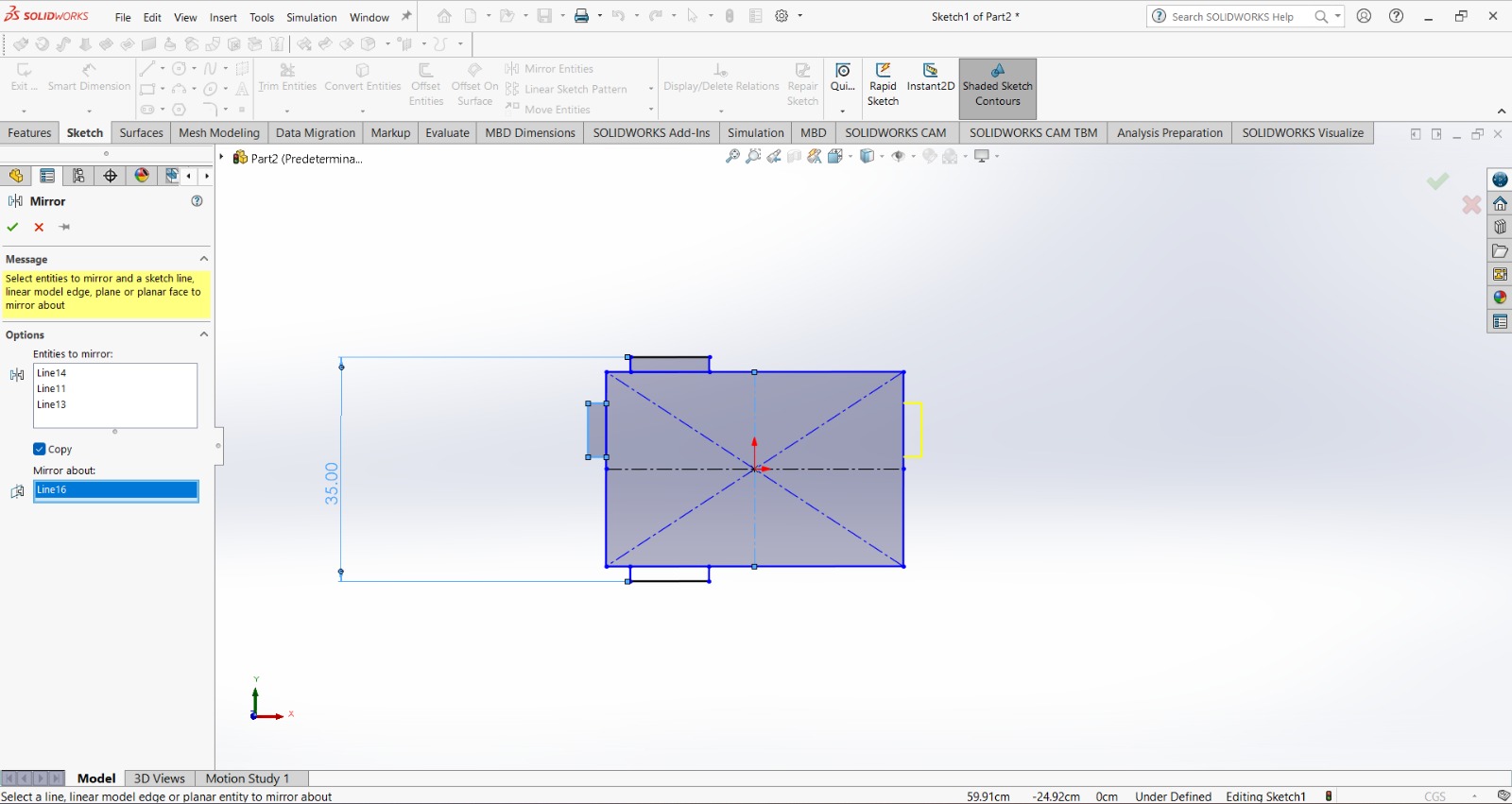
3.After that, I made large finger joint for the lateral faces. For that, I drew a rectangle at the border of 19.5 X mw(1.2 cm) at a distance of 12 cm from the side and center. Then I used the mirror tool to replicate it in both, the opposite side and opposite face. These joints are this thick because they will be joined to the side faces, which are mw thick.
Base
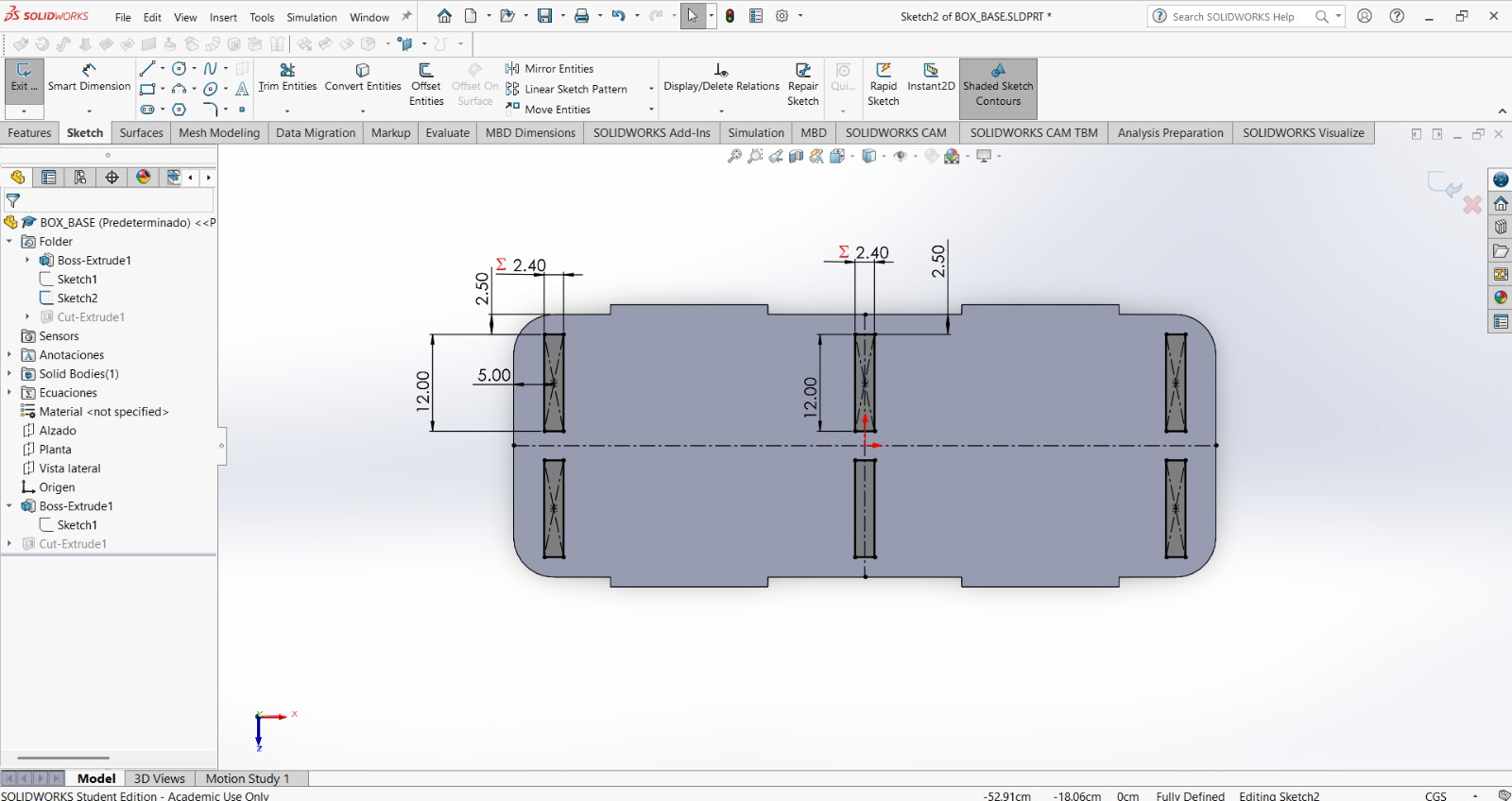
4. Then, I made a rectangle of 2mw X 12 cm at a distance of 2.5 cm from the top border and 5 cm from the side. After that, I used the mirror tool for the 3 columns I planned my box to have. Each wall will consist of two identical pieces of mw thick.
Base
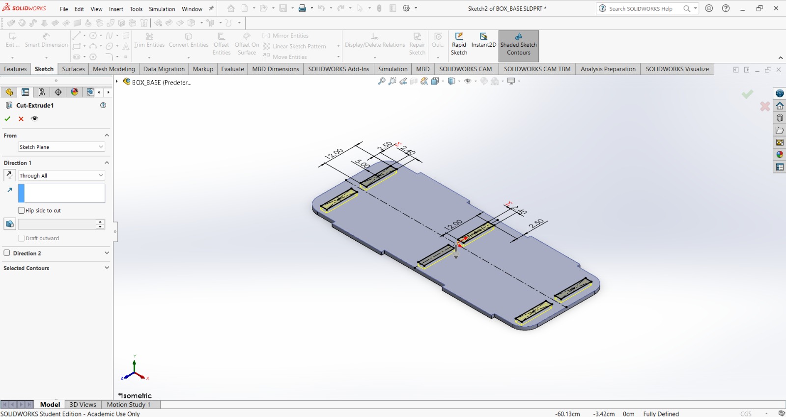
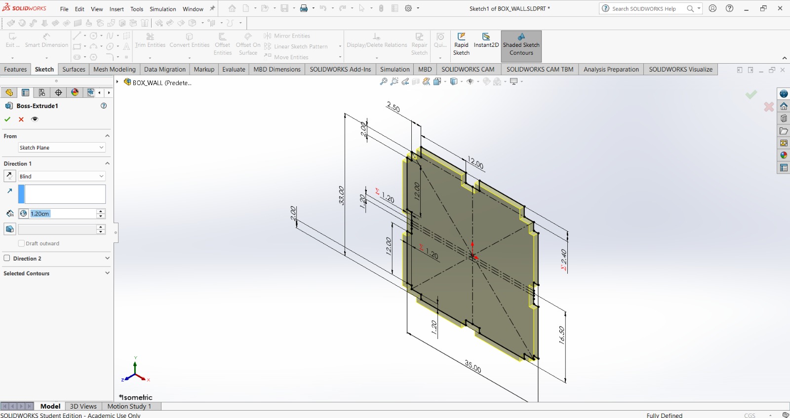
5. Finally I extruded my piece and the cuts.
Lateral Face
Equation.
mw (material width).1.2 cm.
Lateral Face
1. First, I changed the document units to CGS and created a center point rectange of 87X33 cmin the front plane.
Lateral Face
2. Then, using the sketch fillet in all the corners I made arcs of 5 cm.
Lateral Face
3.After that, I followed a similar process to the one for the base. First I made the holes for the columns or interior walls at the same distance as I did in the base, because it was crucial for them to fit on both sides, the base and the sides.
Then, I made center point rectangle at a distance of 10 cm from the left side and 6 cm from the center. Subsequently, I used the sketch fillet tool and made arcs of 5 cm in all the corners of that rectangle. Finally, I used the mirror tool and duplicate it in the opposite side.
This gates will be used to store my dumbells.
Lateral Face
4. Then, I made a rectangle of 19.5 X mw at a distance of 12 cm from the side and center. After that, I used the mirror tool for duplicate it in the other side. These rectangles will be to join this side face to the base.
Lateral Face
5. Finally I extruded my piece and the cuts.
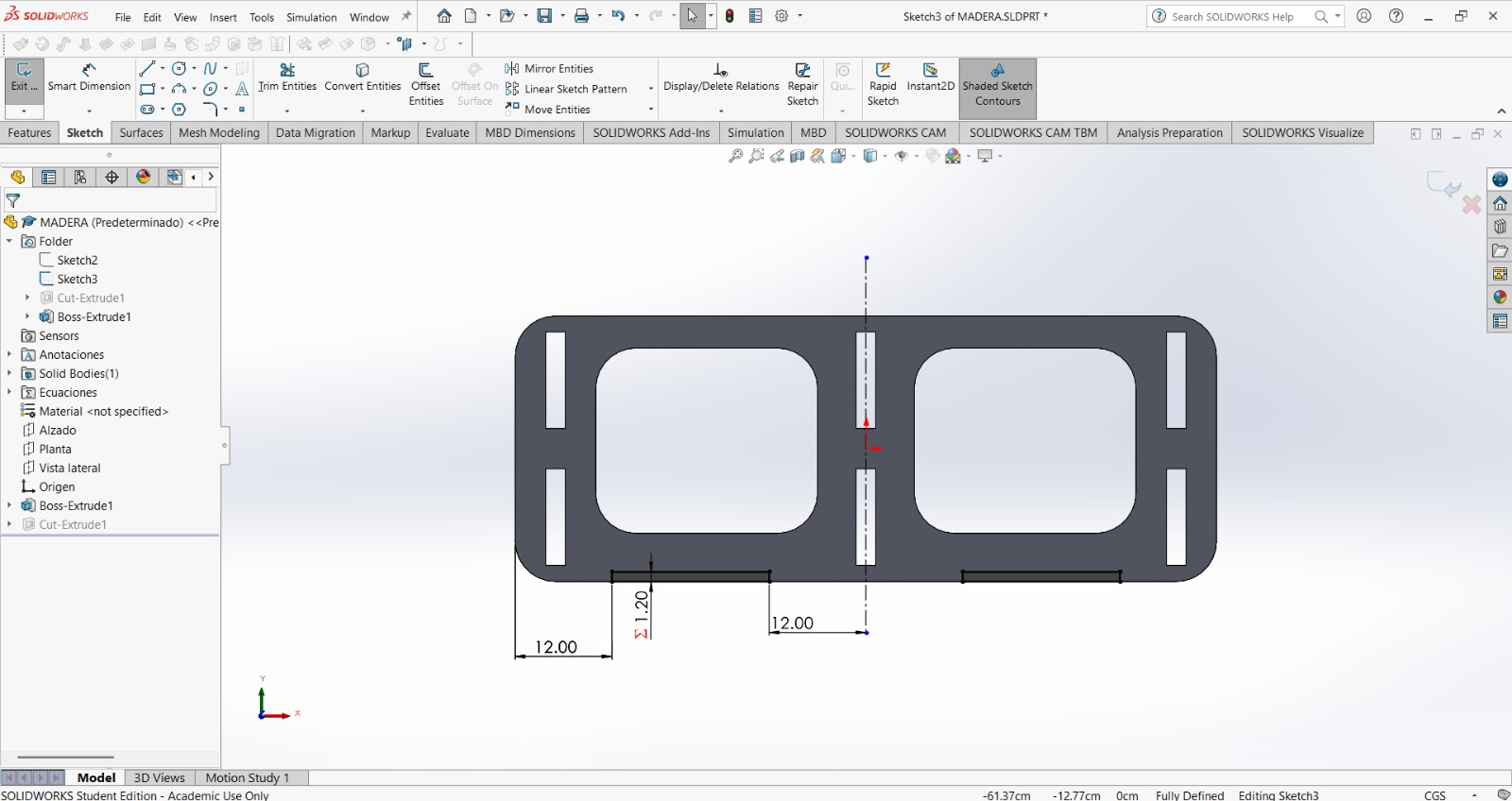
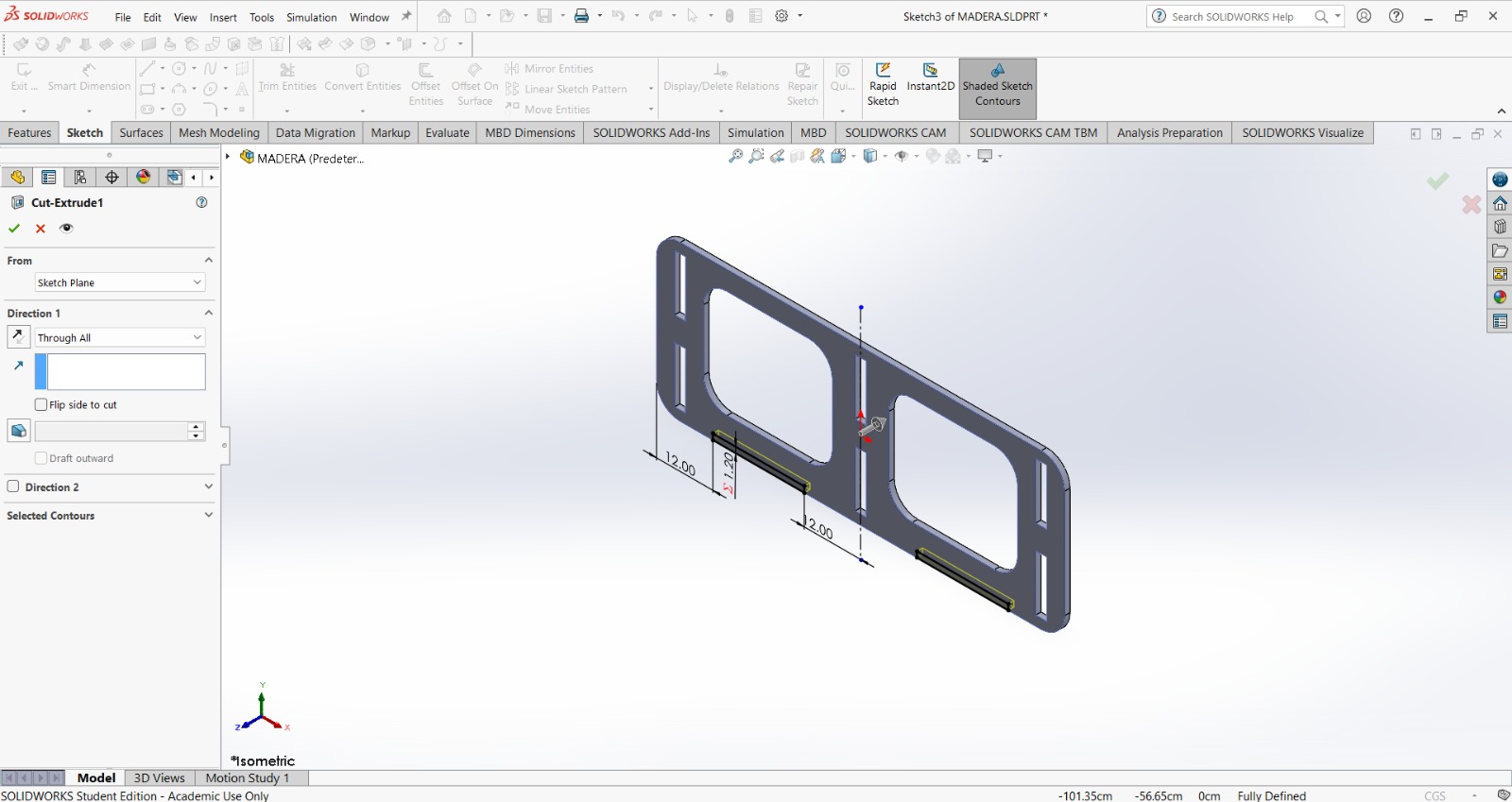
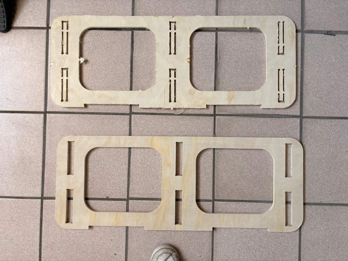
Wall - Column
Equation.
mw (material width).1.2 cm.
Wall - Column
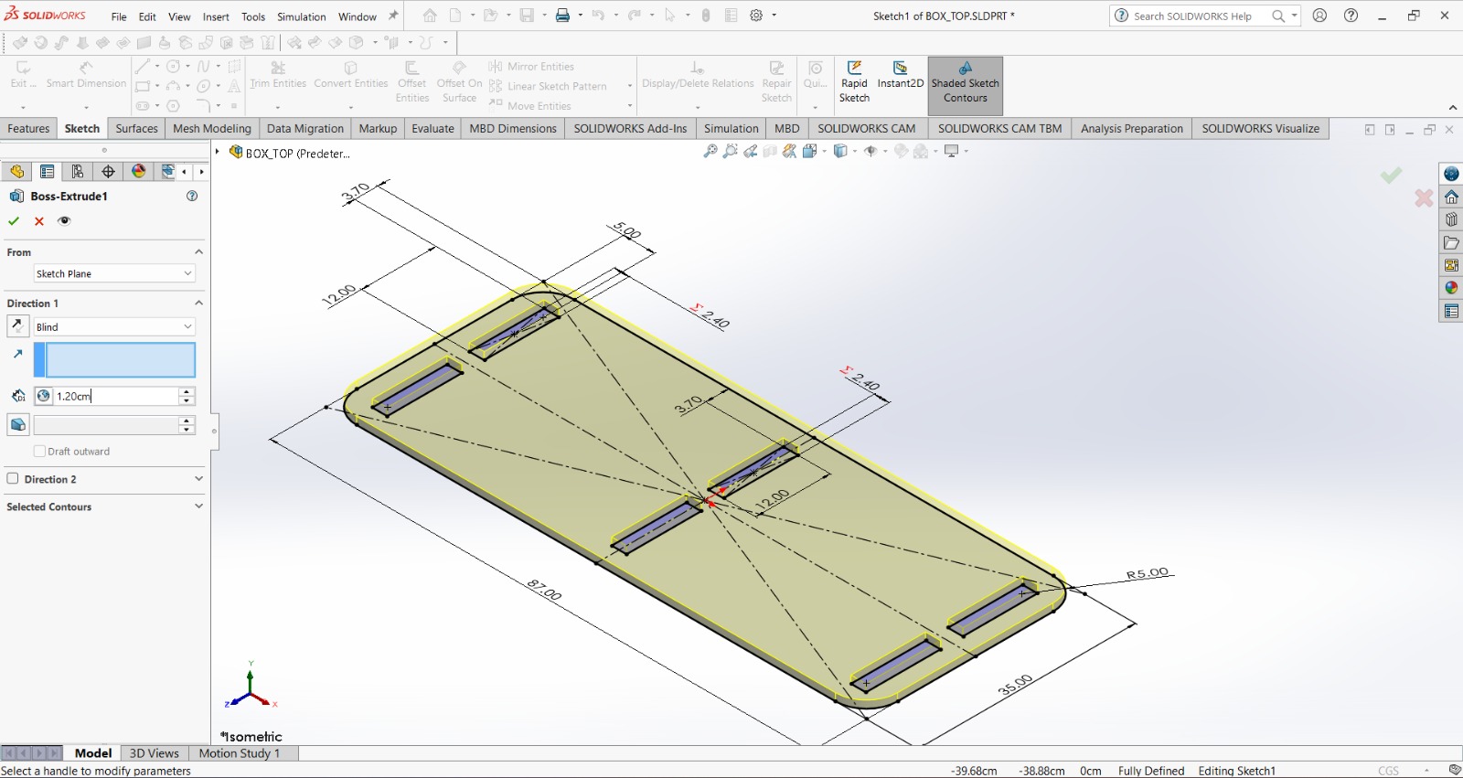
1. First, I changed the document units to CGS and created a center point rectange of 33 X 35 cmin the front plane.
Wall - Column
2. Then, I made two rectangles at the top and left border and mirror them.
Wall - Column
3. All of the joints have a height of mw with the exception of the top ones, those have a height of 2 mw because in the top will be two layers, each of mw. Each finger joint has a width of 12 cm.
In the sides, the distance between the finger joints and the bottom is of 2 cm. In the top, the distance between the joints and the sides of the rectangle is of 2.5 cm.
Wall - Column
4. Then, I made a circle of 0.78 cm of diameter at a distance of 15 cm vertically and 13 cm horizontally from the center. After that, I used the mirror tool for duplicate it in the other side and down. These holes will be for M8 screws that will connect the two pieces I’ll have for each column.
Wall - Column
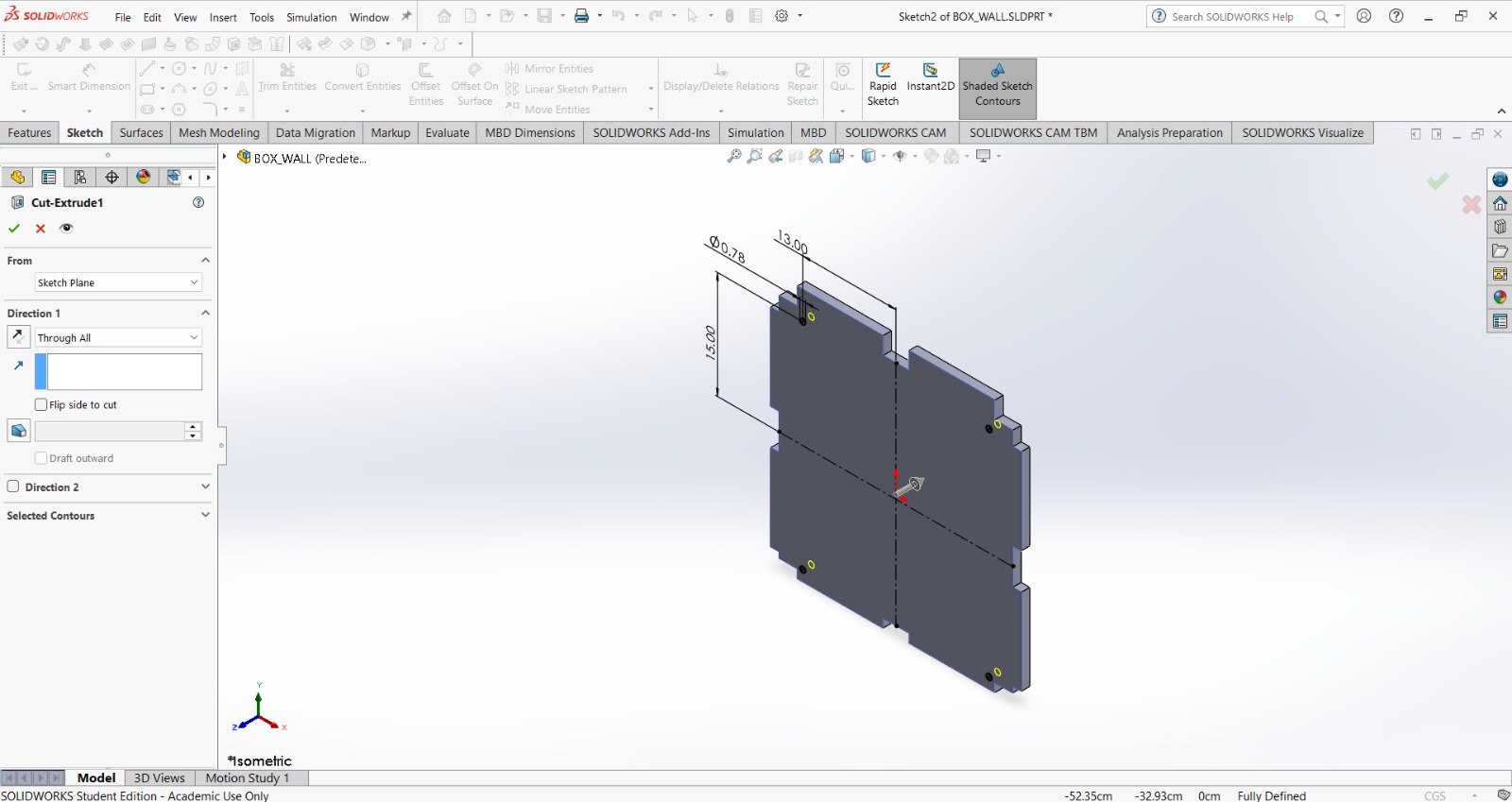
5. Finally I extruded my piece and the cuts.
Top cover
Equation.
mw (material width).1.2 cm.
Top cover
1. First, I changed the document units to CGS and created a center point rectange of 35 X 87 cmin the front plane.
Top cover
2. Then, using the sketch fillet in all the corners I made arcs of 5 cm.
Top cover
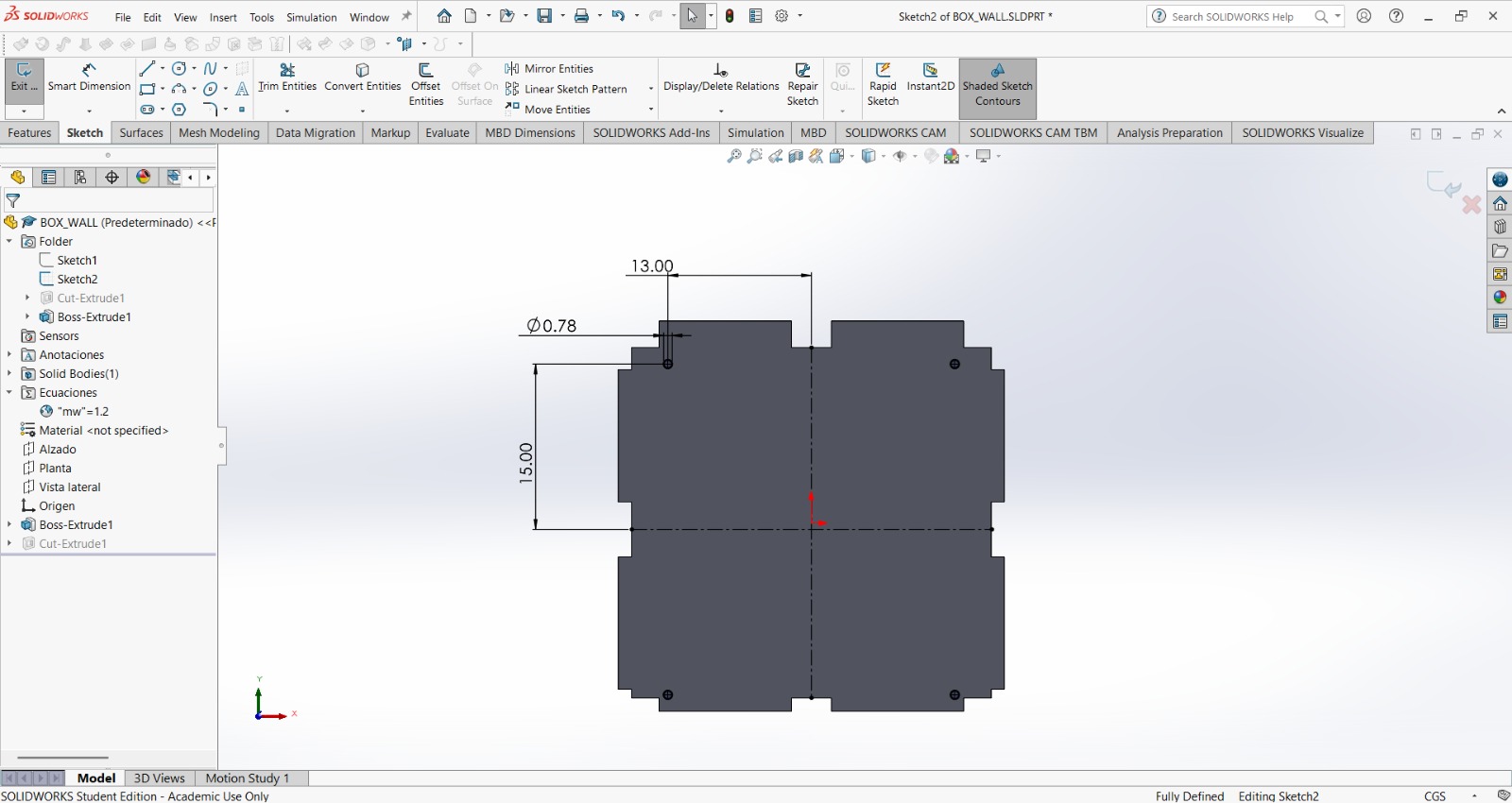
3. Then I made the same holes of 2mw width, I did in the base.
Top cover
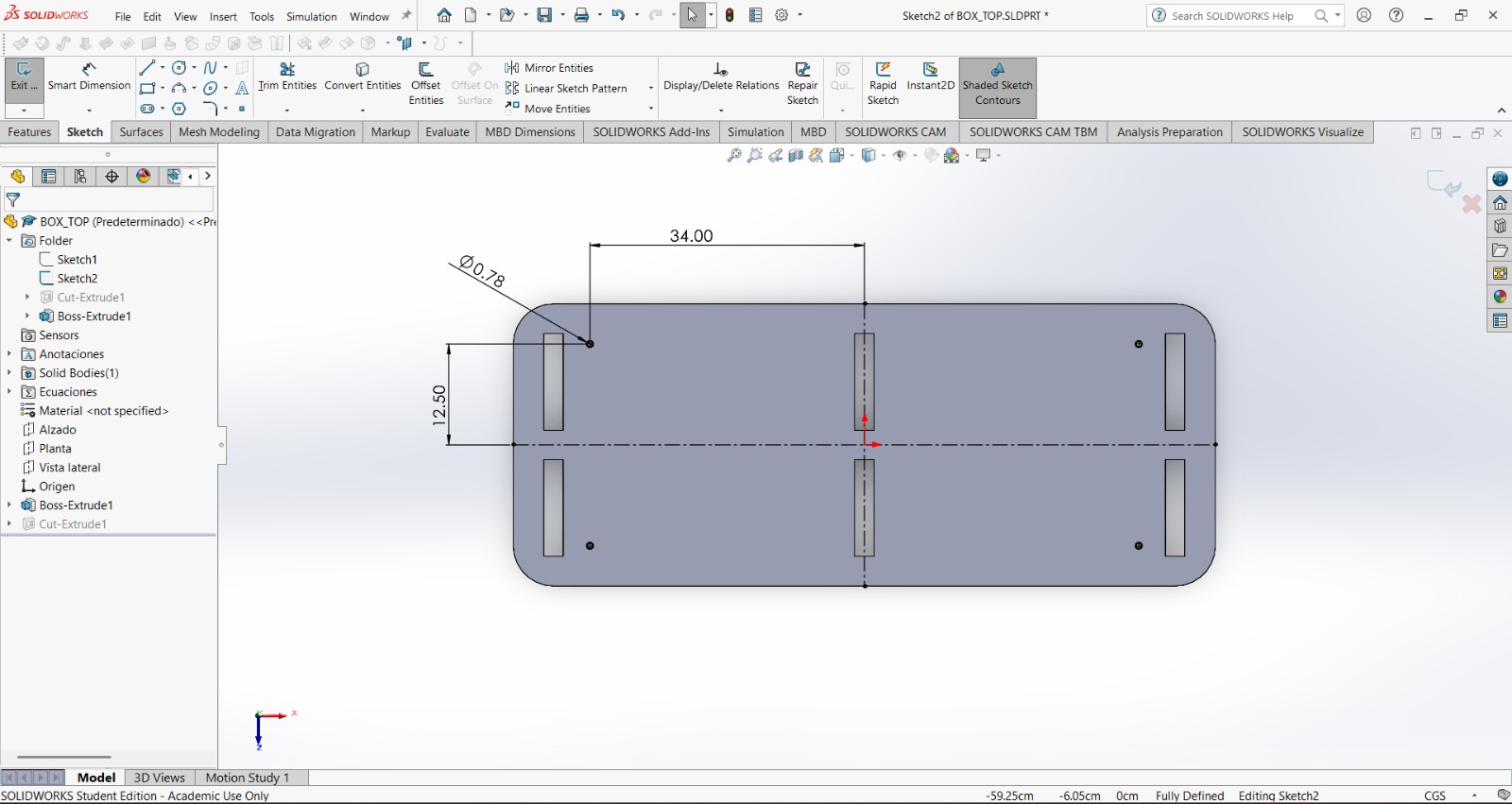
4. Then, I made a circle of 0.78 cm of diameter at a distance of 12.5 cm vertically and 34 cm horizontally from the center. After that, I used the mirror tool for duplicate it in the other side and down. These holes will be for M8 screws that will connect the two pieces I’ll have for each column.
Top cover
5. Finally I extruded my piece and the cuts.
Exporting as DXF
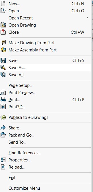
1. First we have to click on File, located at the left top corner, and select save as in the menu.
Exporting as DXF
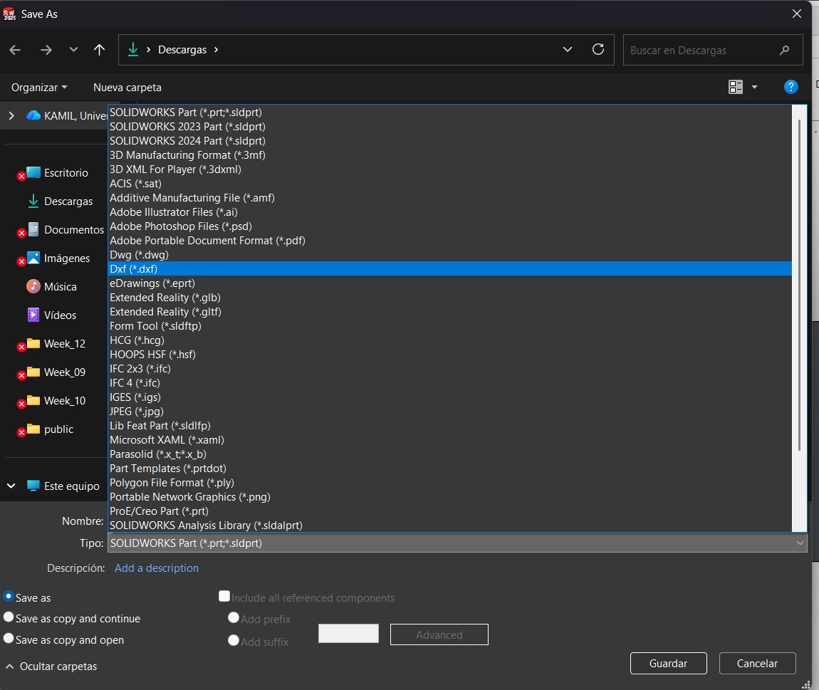
2. Then we have to click on the Document type tab, look for DXF and select it.
Exporting as DXF
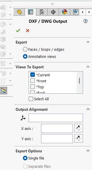
3. After that a lateral menu will deploy and there we can choose the plane where our pice will be saved in the DXF document.
Exporting as DXF
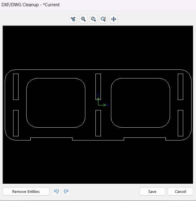
4. Finally a preview of our document will be shown. After that just have to save it.
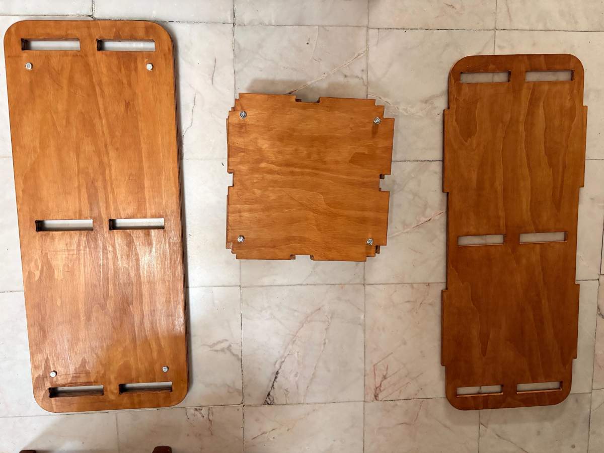
Results
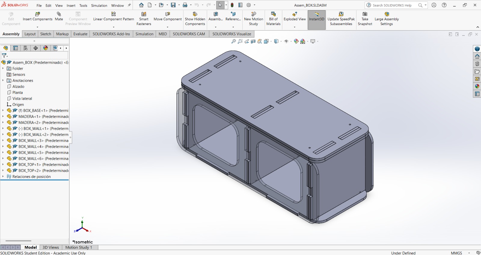
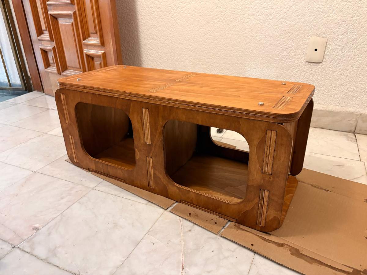
RESULTS.I made an Assembly with all the pieces to make sure everything was correct.
Fabrication
VCarve
VCarve, developed by Vectric, is a popular, user-friendly software solution designed for designing and cutting parts on CNC routers. It excels at 2D design, 2.5D machining (V-carving, pocketing, drilling), and importing 3D models. It is widely used for sign-making, woodworking, and engraving, allowing users to create complex, carved 3D effects from 2D vectors.When used alongside a CNC router, VCarve serves as the bridge between the design phase and the actual production process. While CAD programs like SolidWorks are utilized to create the part designs, VCarve focuses on setting up machining details such as toolpaths, cutting settings, tool choices, and strategies, ultimately generating the G-code that controls the CNC machine.
VCarve
1. First we have to open VCarve and create a new file. In the left menu is a list where we must select the first option.
VCarve
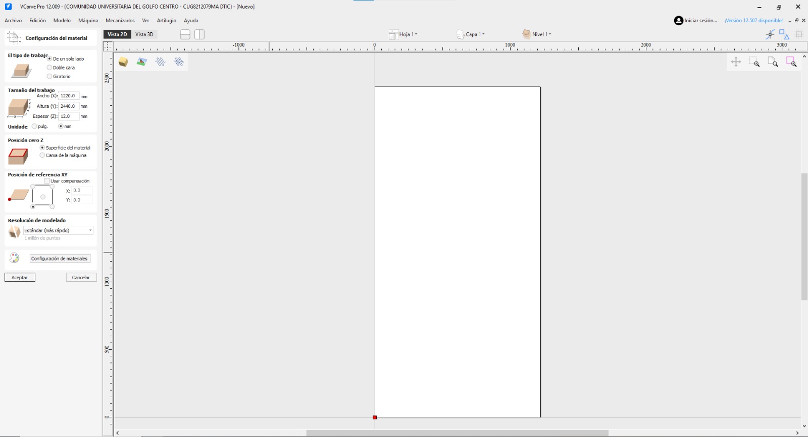
2. Then, a workspace will pop up and in the left side we can choose the characteristics of our board and where to set the origin point.
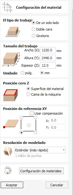
Configuration.
Work Type.Defines the machine type in one side mill, two sides mill, Rotating. In this case, I´ll choose the first option, because the machine I will be using is the Mach 2/3 Arcs router that only has 3 axis (x,y,z) so it can mill up to 2.5D pieces.
Work Size.Defines the board size. In my case, my material size is of 1.220 X 2440 X 120 mm.
Z origin position.Sets the initial position for Z. It can be either at the top of the material or at the top of the top of machine surface.
Reference Position for XY.Sets the reference origin position for XY. In my case, it will start a the bottom left corner.
Resolution.Defines the resolution for the simulation.
Material Configuration.Defines the material appearance for the simulation.
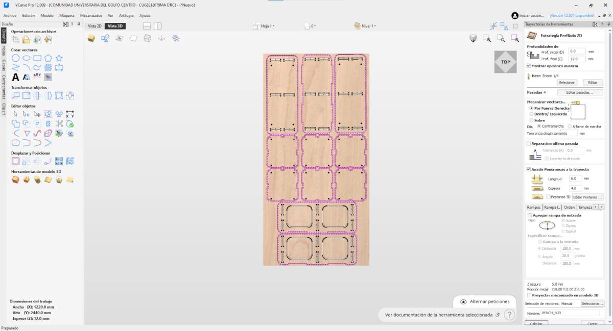
VCarve
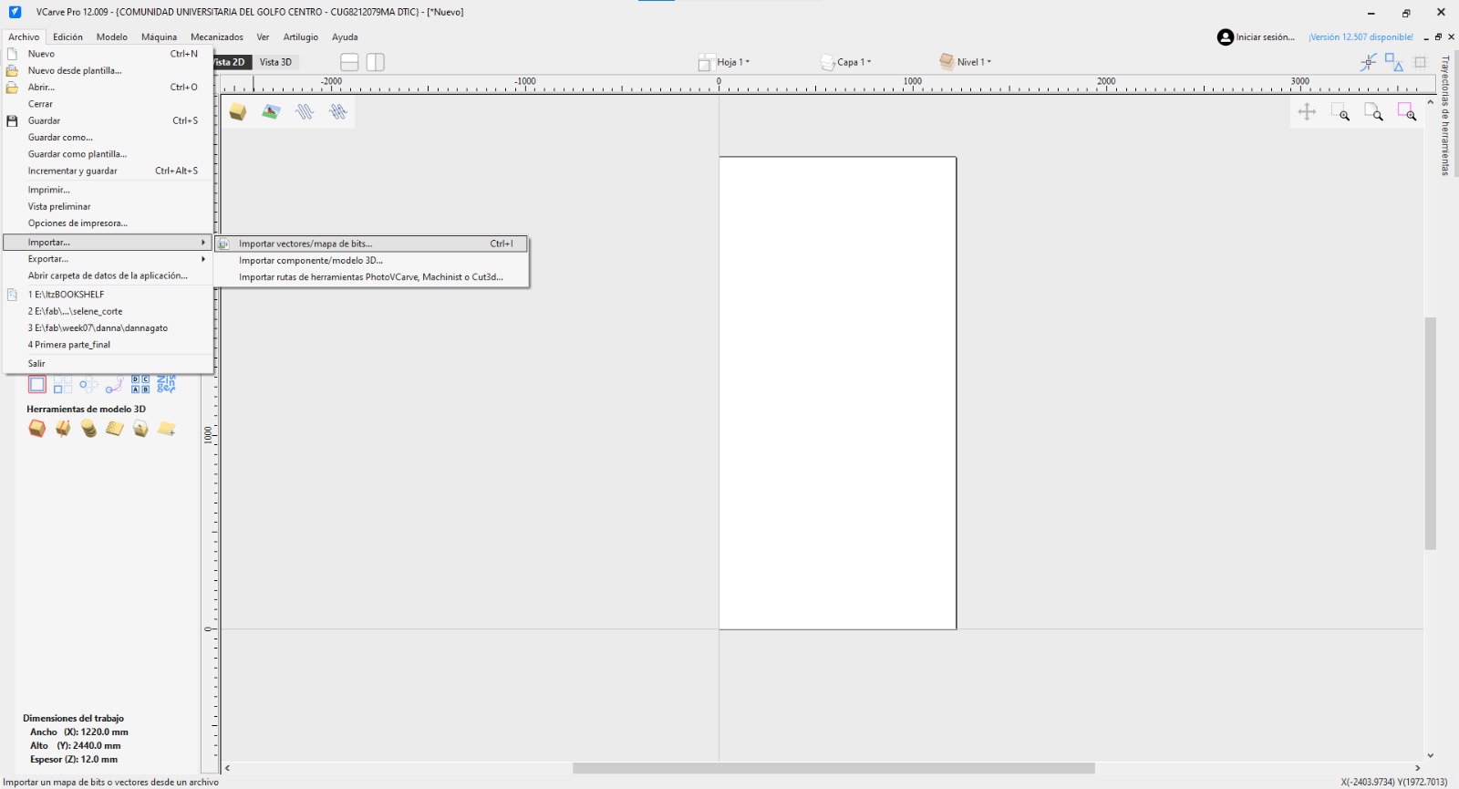
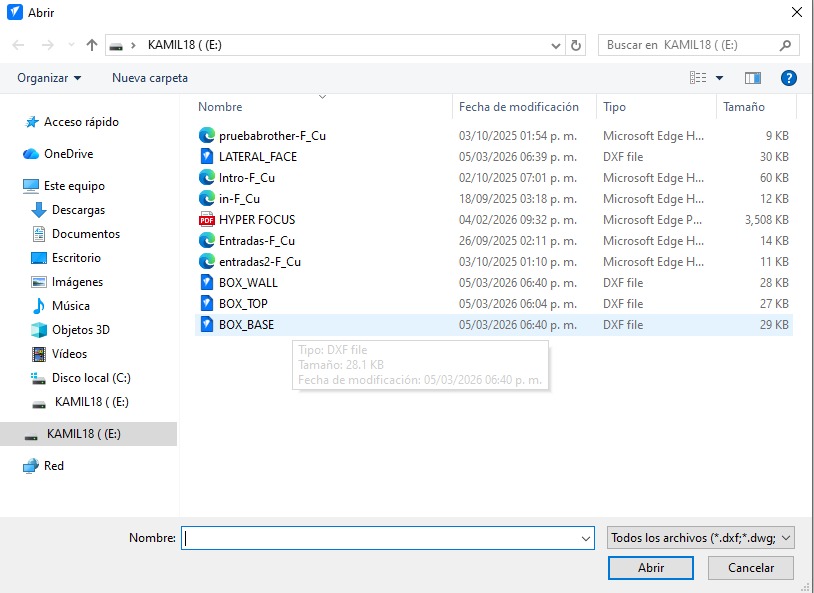
3. Then we have to click on FILE and Import. Later, we have to choose te file we want to import, in my case here are my 4 pieces.
VCarve

4. Then we have to add our pieces and placing them in the board. At the corner of each piece is a symbol to rotate the figure.
VCarve
Fillets - Dog Bone
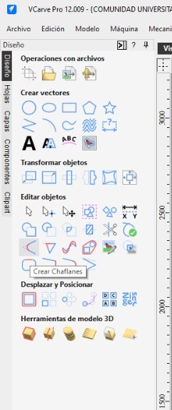
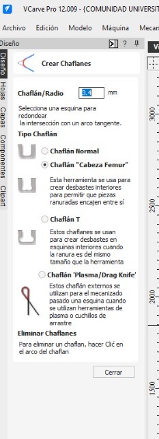
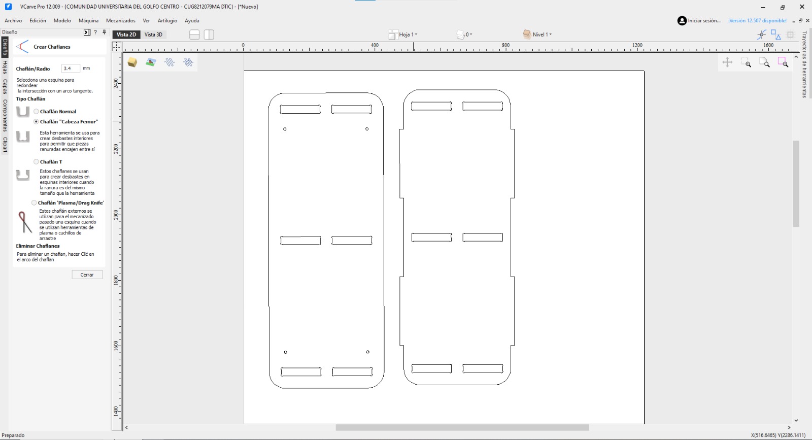
5. After placing all our pieces, we have to do fillets in the perpendicular internal corners, this is with the pourpose of making an easier path for the machine and also will help to fit the pieces in each other.
Dog-Bone.
This fillet type allows square parts to properly fit into internal corners that are machined with a round cutting tool.
Properties
The radius of my fillets is 3.4 cm.
VCarve
Join vectors
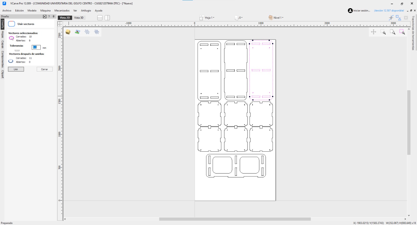
7. Some pieces don't have all of its vectors together, for that we can use the Join vector tool that is located down the Fillet tool.
Join Vector. To join the vectors we only have to group them with the tool and then click join.
VCarve
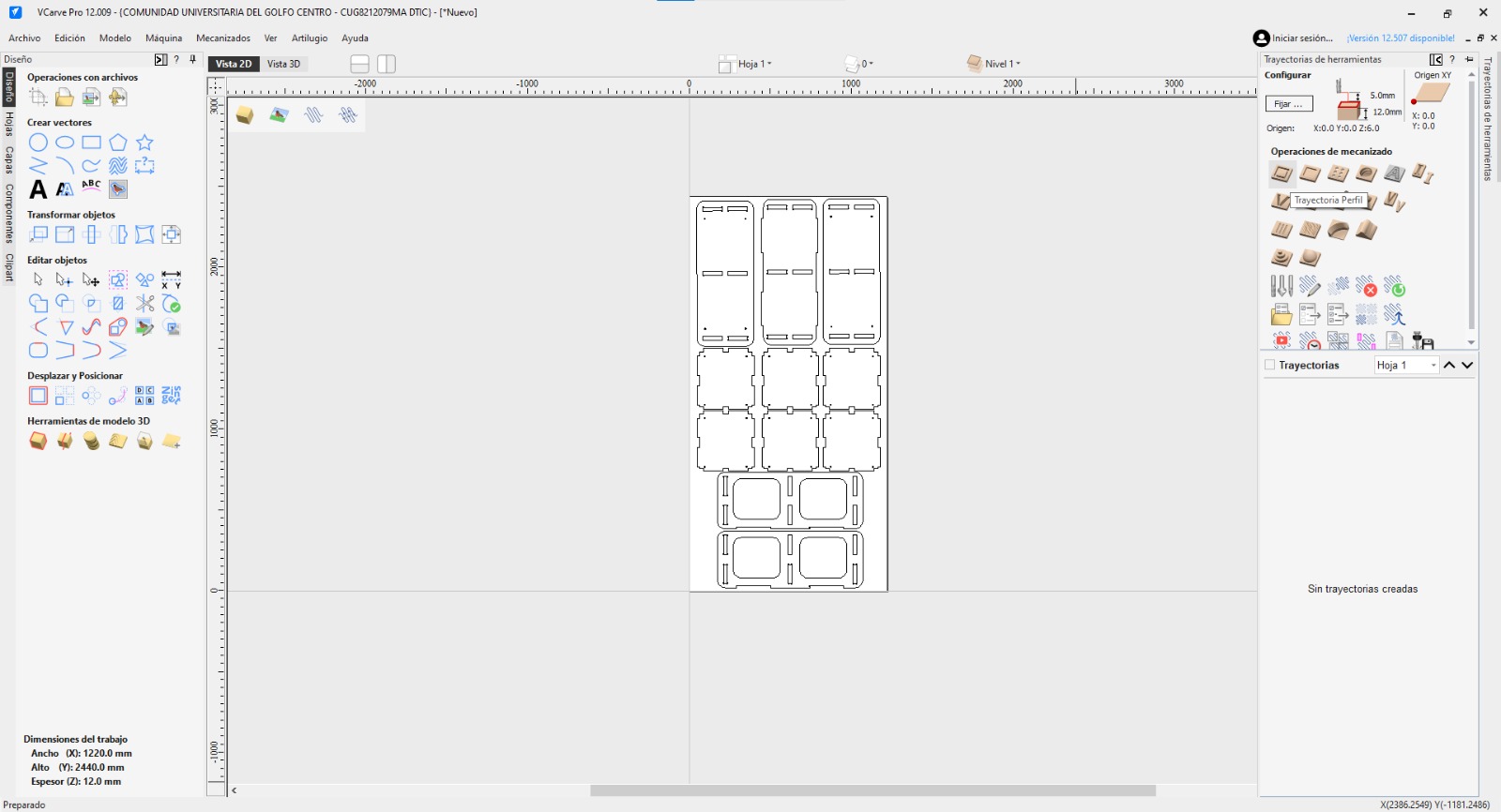
8. Once all the pieces are in place, the vectors are connected, and all the dog bones are done, the next step is make the external and internal cut. For that, we have to select Tool trayectory, which ist the first symbol in the right side menu.
VCarve
Milling cutter
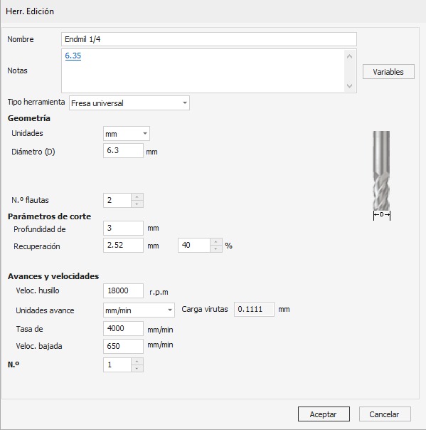
Milling cutter. This Parameters are specifically for the tools we have in our Lab in Puebla.
Milling cutter.
Diameter. 6.3 mm - 1/4 inch
RPM.18000
Feed Units.mm/min
VCarve
External cut
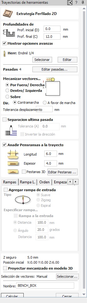
External Cut.For the outer cut, the first parameter to set is the cutting depth. In my case, my material is 12 mm thick, so that is the depth I set, starting the cut at height 0.
The next important parameter is where the cut will begin; Vcarve offers three options: outer, inner, or over.
In this case, I will start from the outside in a counter-climb direction because it yields better results.
Finally, it is necessary to add tiny bridges to prevent the part, when cut from the outside, from detaching from the material and being damaged by the passing milling tool.
VCarve
Internal cut
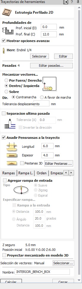
Internal Cut.For the internal cut, the first parameter to set is the cutting depth. In my case, my material is 12 mm thick, so that is the depth I set, starting the cut at height 0.
The next important parameter is where the cut will begin; Vcarve offers three options: outer, inner, or over.
In this case, I will start from the inside in a counter-climb direction because it yields better results.
Finally, it is necessary to add tiny bridges to prevent the part, when cut from the outside, from detaching from the material and being damaged by the passing milling tool.
VCarve
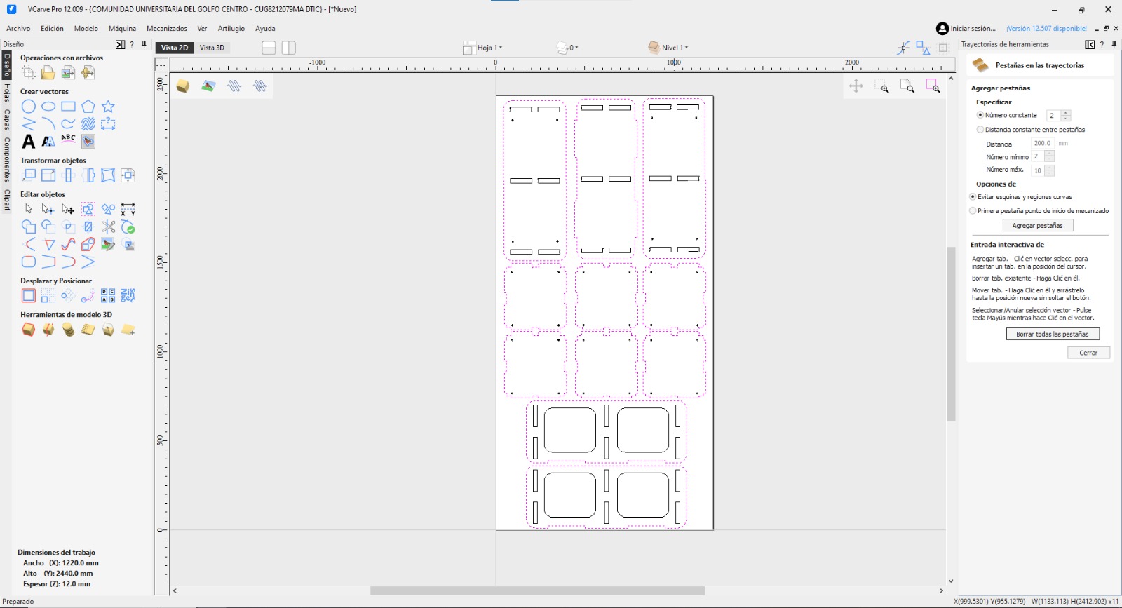
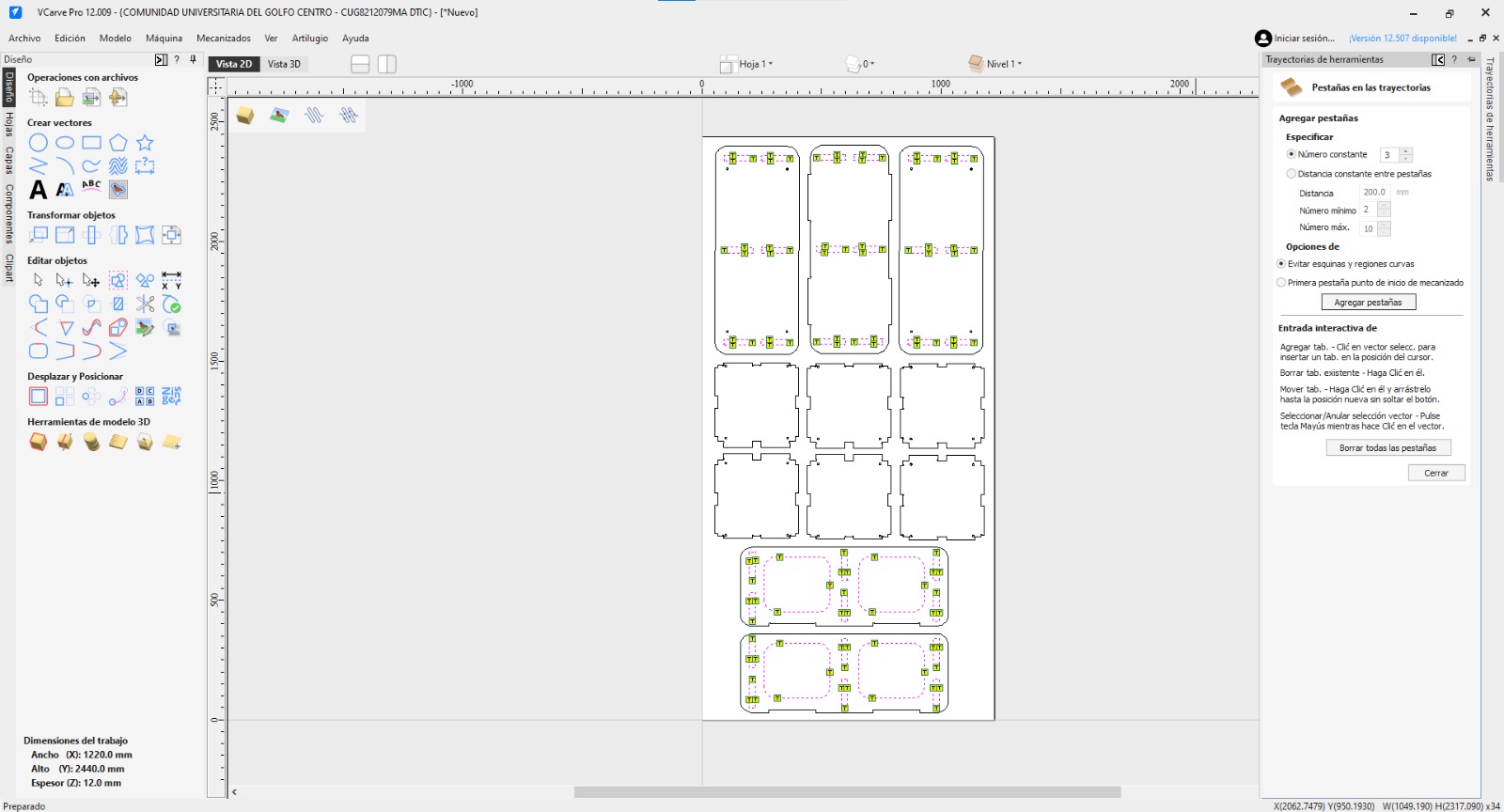
Bridges
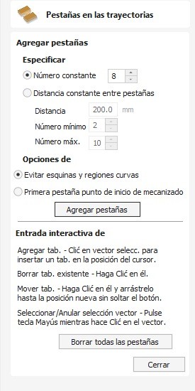
Bridges.To add bridges, go to the “Tool Trajectory” section and select whether you want to add bridges. A small menu will then appear where you can choose how many to add; in the image, 8 are selected, but I used 4 in my parts. The bridges are placed automatically when you click “Add Tabs.”
Recomendation. The separation between two pieces must be more than 23 mm, in order to have more grip to the board.
VCarve
Export
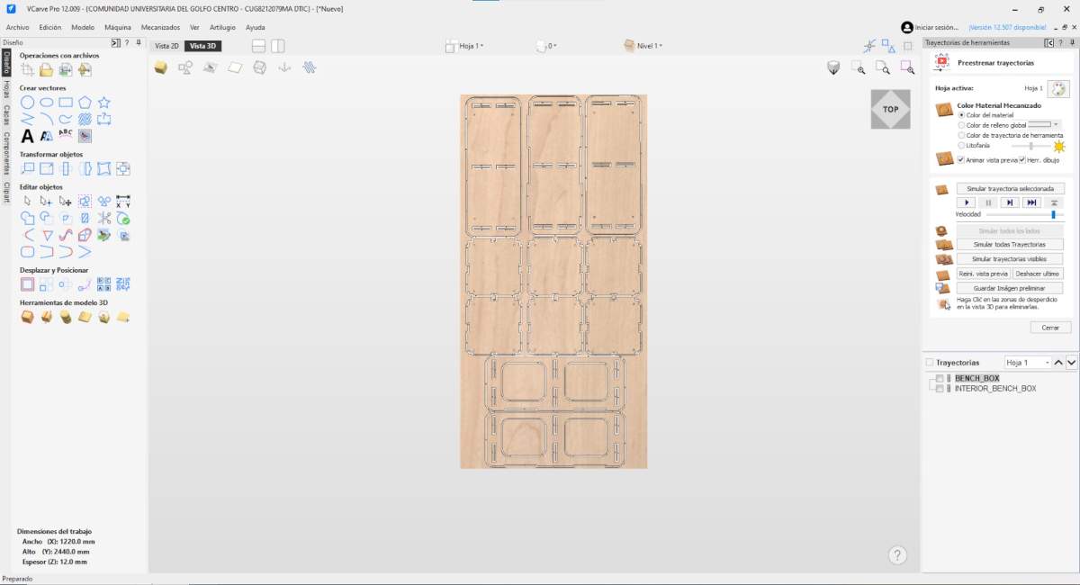
9. The next step is export the toolpaths in the preview window. This feature allows the user to simulate the machining process and provides a 3D visualization of the material after the cutting operations.
If the project contains multiple toolpaths (as in this case), they can be reordered by dragging them within the toolpath list, allowing the user to prioritize the order in which the CNC machine will execute each operation. For save the G-code we need to:
Click on "Save Toolpath".
Format. Depending on the machine we will use, we can save it for the Mach 2/3 Arcs (mm) (*.txt) and for the Asia Robotics.
Machine
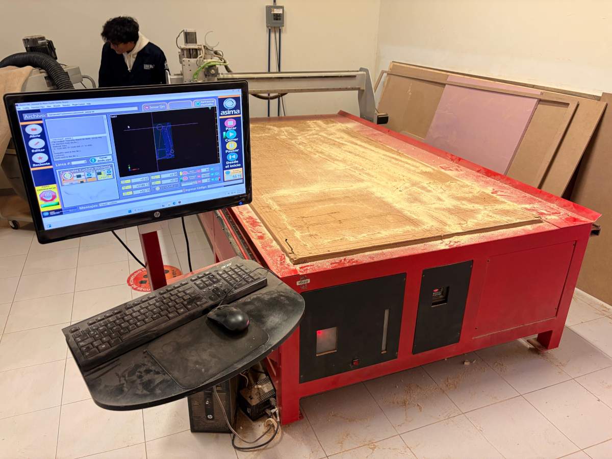
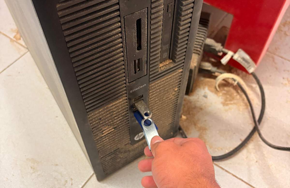
1. The machine I used was the Mach 2/3 Arcs router. The first step is to turn on the computer and place our file in it.
Safety measures. It is important to wear a lab coat, boots and some protection for the eyes during this process.
Machine
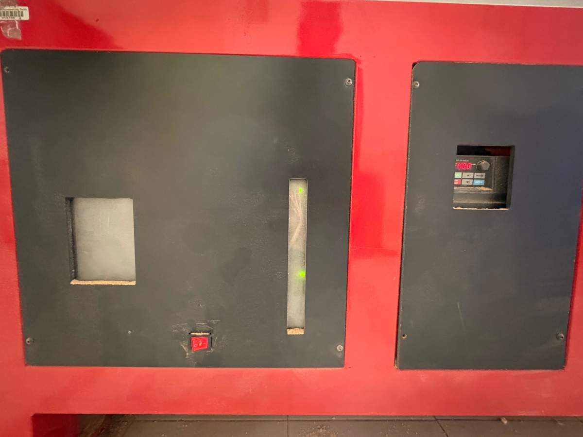
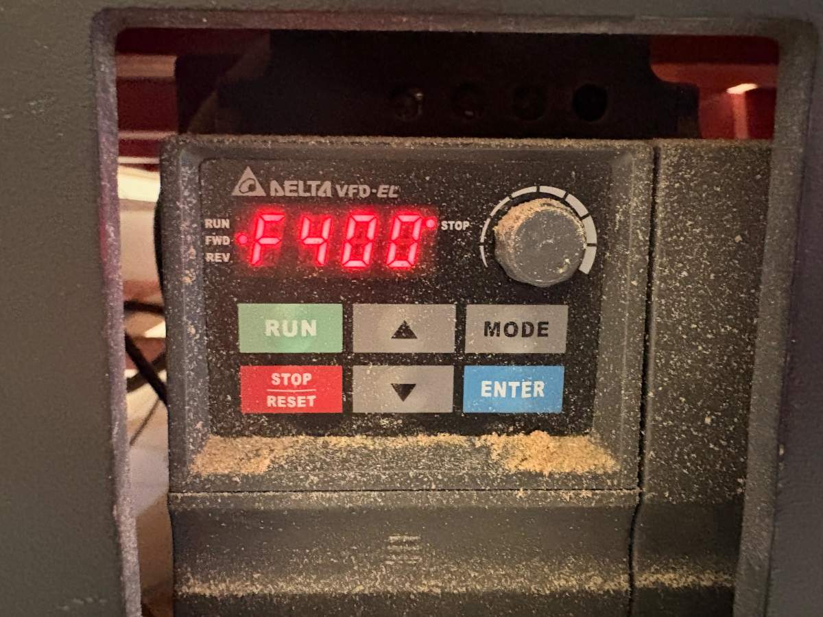
2. To turn on the router CNC we have to press the red button and make sure the variable frequency drive is on.
Machine
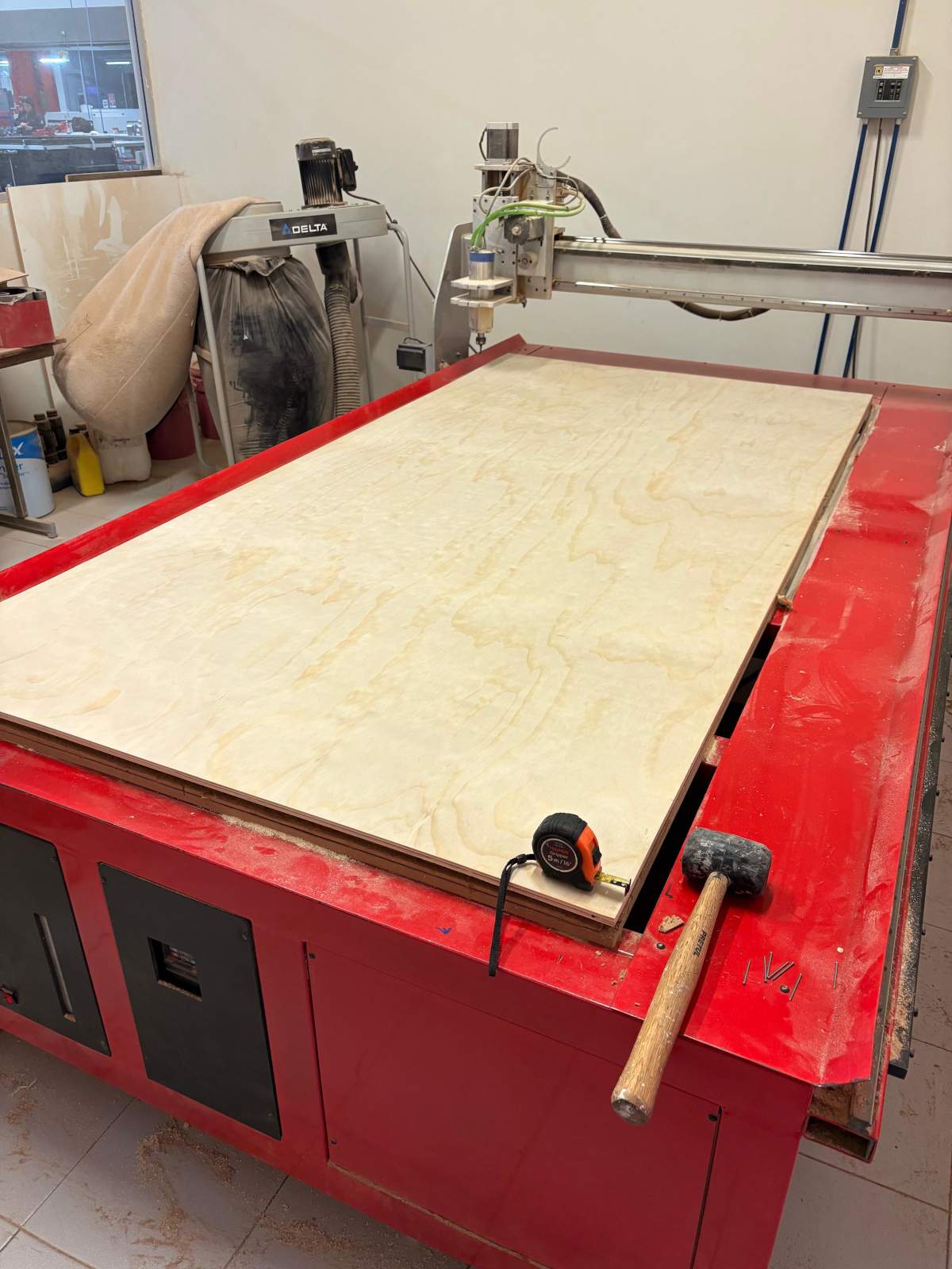
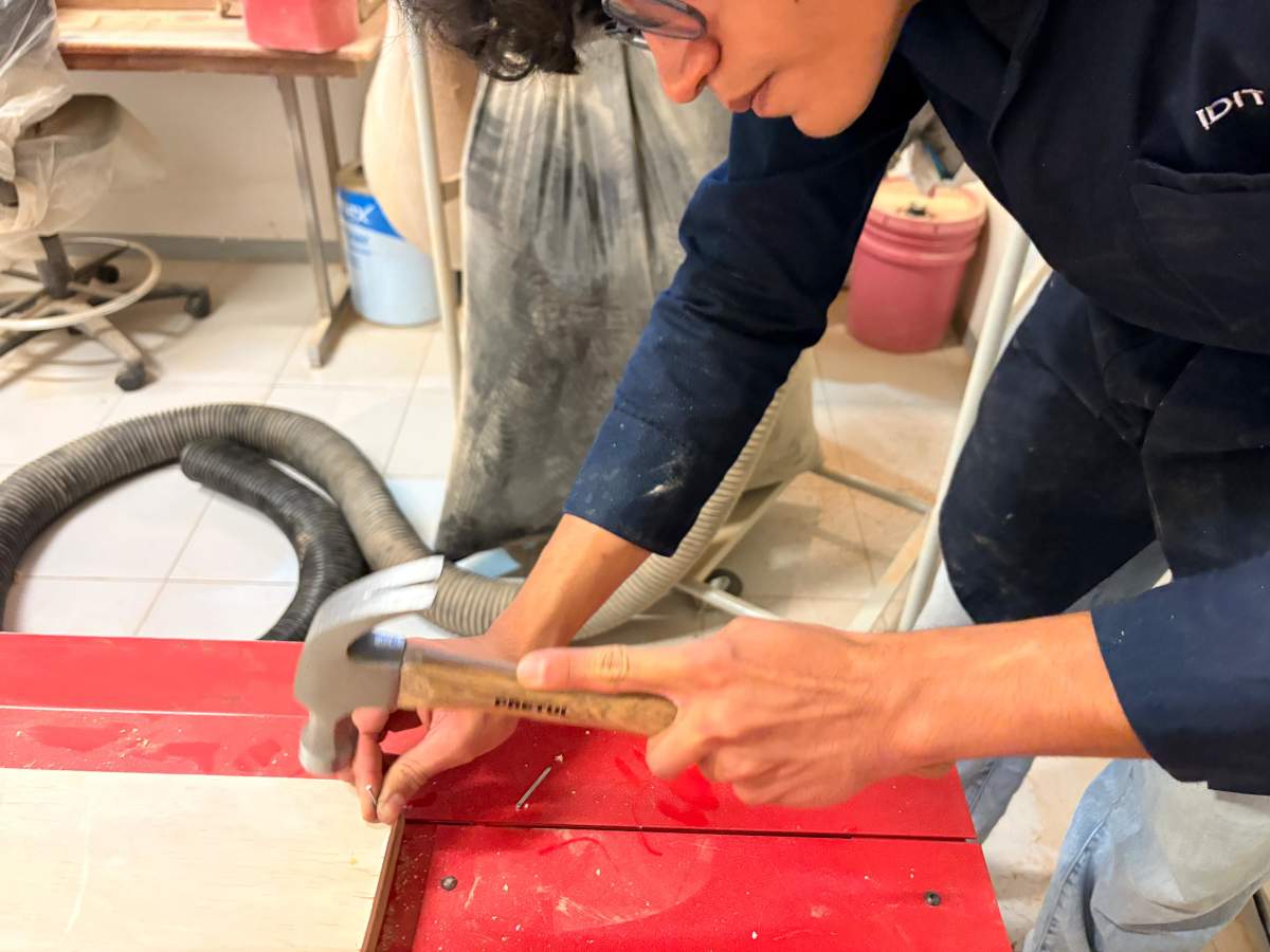
3. Then we have to place our board over the sacrifice bed (spoilboard). To prevent the material from moving during cutting and for safety reasons, the board is fixed to the base with nails. This ensures that the material remains completely immobile while the CNC tool is in operation, thereby preventing potential machining errors or accidents.
Machine
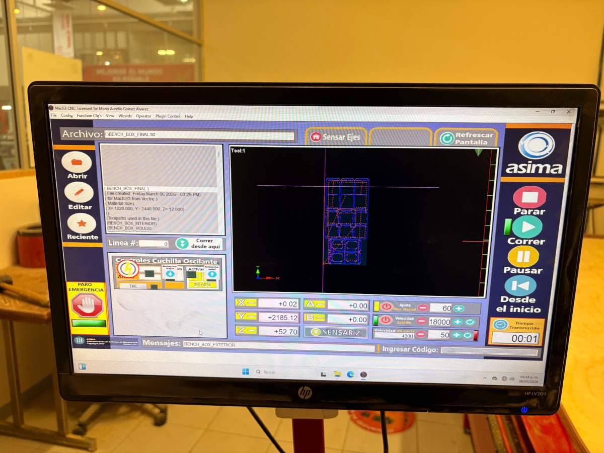
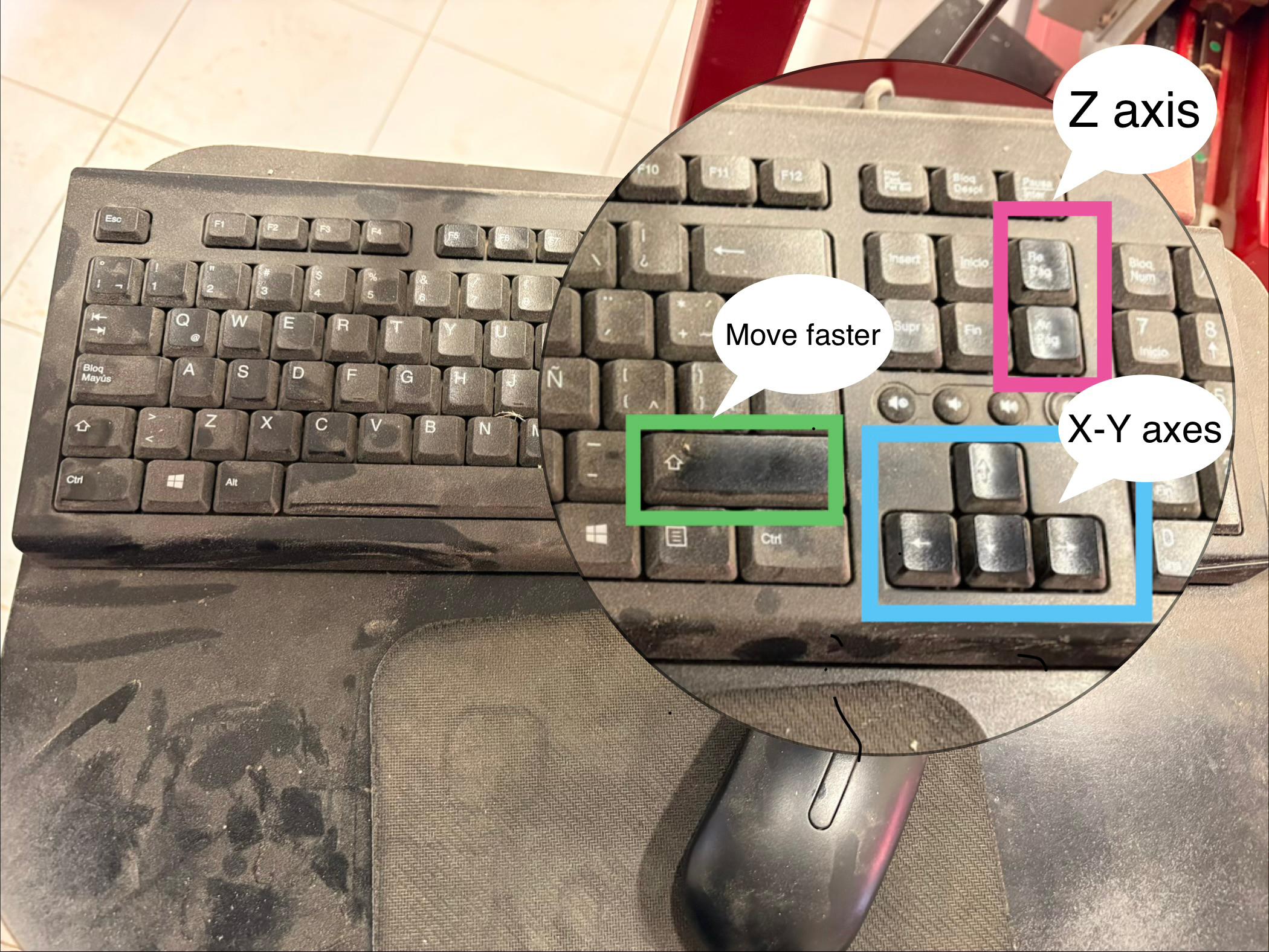
4. The program used to operate the CNC machine is AR2400. After opening the program, we have to open our file, make sure the parameters are correct and the run it. The CNC machine can also be controlled using the keyboard.
AR2400 Sections.
Open FILE. Is the first circle in the left side. This option allows you to import the G-code file that the CNC machine will run. The file can be loaded from a connected USB drive or directly from your computer.
G CODE. This is the wide rectangle section with code next to the Open FILE symbol. This section displays the lines of G-code that the machine is currently executing. It also allows the user to select or set the starting line of the program if needed.
Piece visualization.It is the large rectangle that shows the piece the machine will cut.
Axes.Down the Piece visualization section are the axes of the machine. Here we can control and monitor the position of the tool. The yellow buttons allows us to set the origing in each axis.
Cutting Speed.This section allows you to manually control the machine's movement, adjusting the spindle speed (RPM), feed rate and travel speed.
Controls.This area contains the controls used to run, pause, stop, or restart the machining program. It also displays the amount of machining time that has elapsed.
Machine
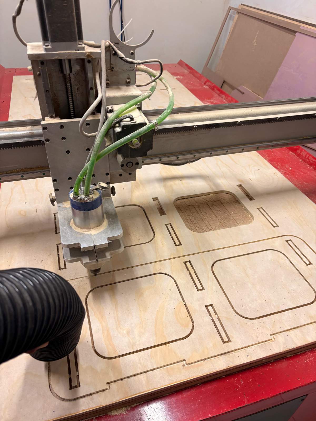
5.After the machine origin has been correctly set and the CNC program begins execution, the machining operation must be monitored at all times. As the cutting tool moves through the material, it produces large amounts of sawdust and wood debris. Allowing this material to build up near the cutting zone may create a fire hazard because of the heat and friction generated by the spinning tool. Therefore, the debris should be removed continuously, commonly with a vacuum or dust collection system, particularly around the areas where machining is taking place.
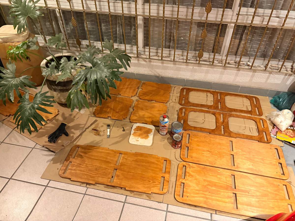
Painting
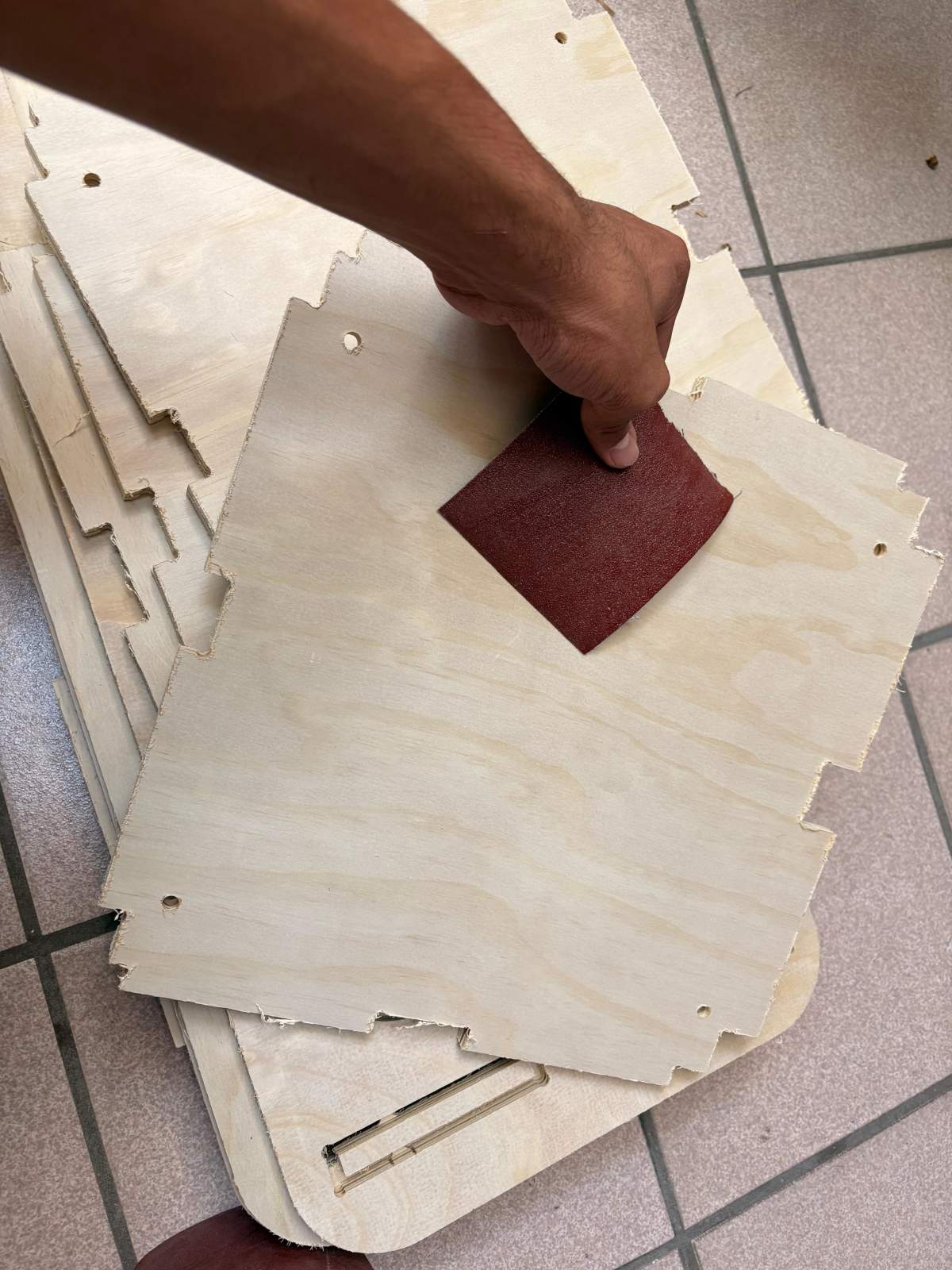
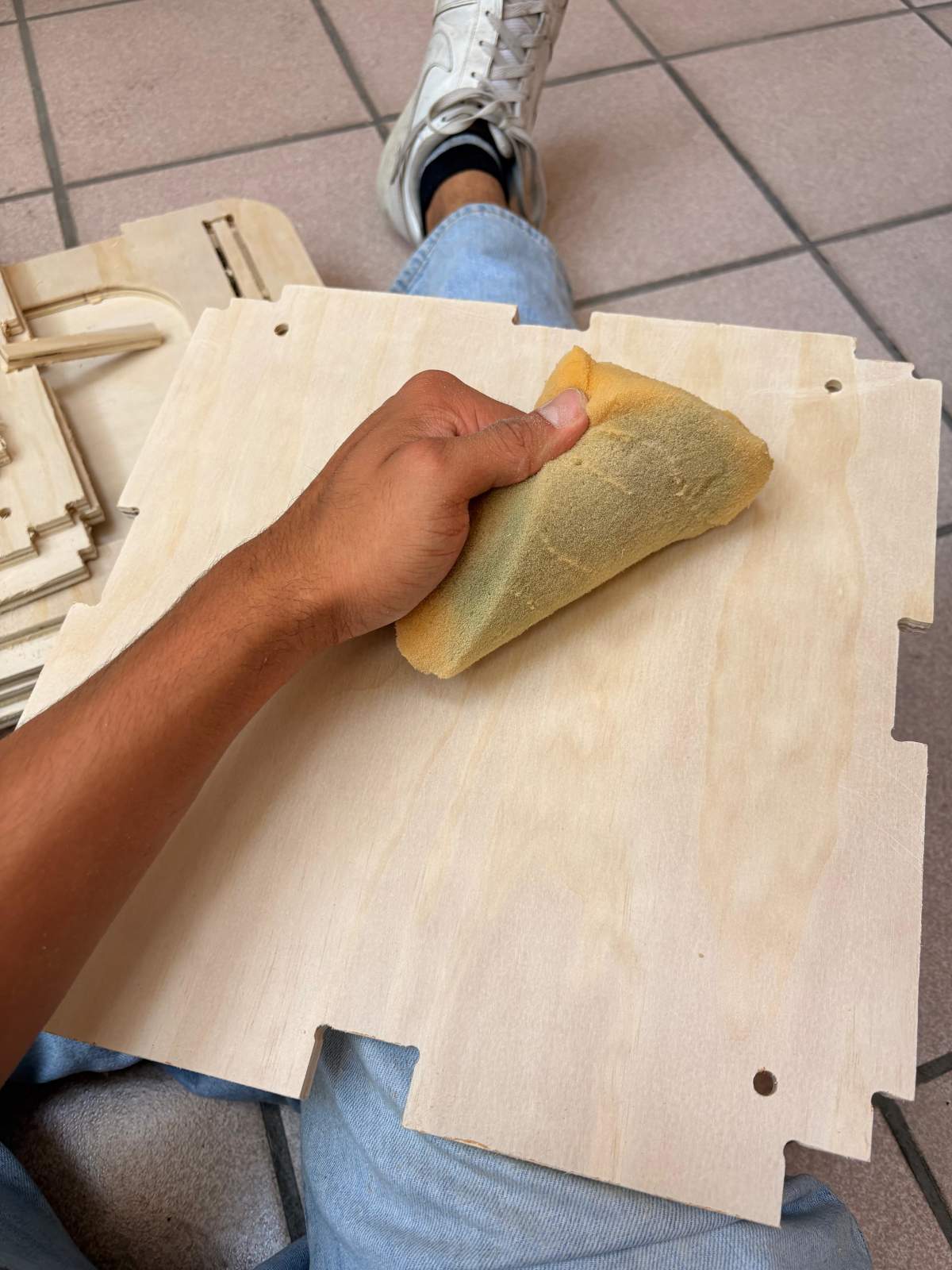
1. First we have to gather all of our pieces and sand the down.
Painting
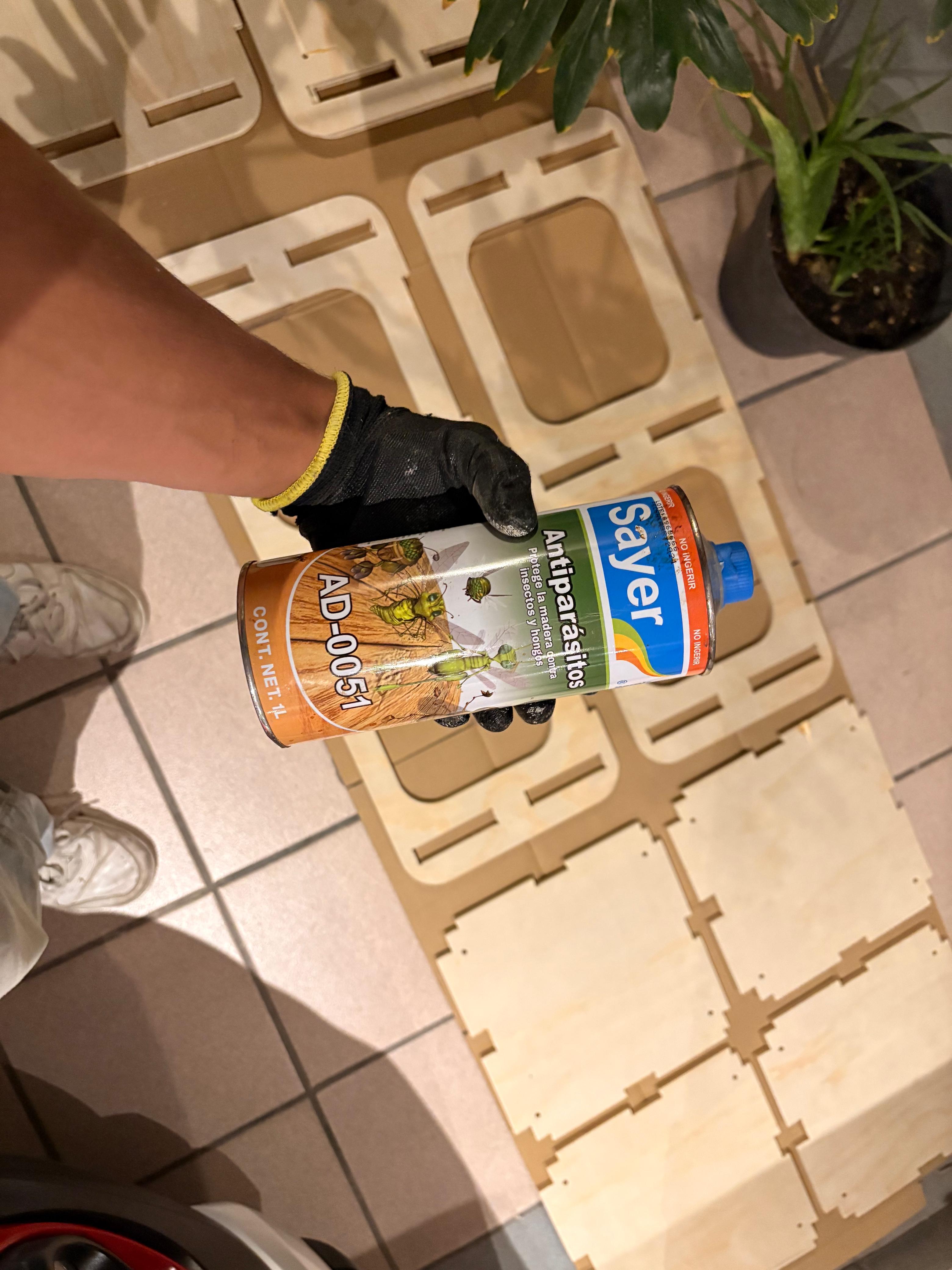
2. Having sanded all our pieces we need to use some anti insects product. Which is a product specially formulated to protect wood from insect damage. To apply it we just have to use some cloth and wear gloves.
Painting
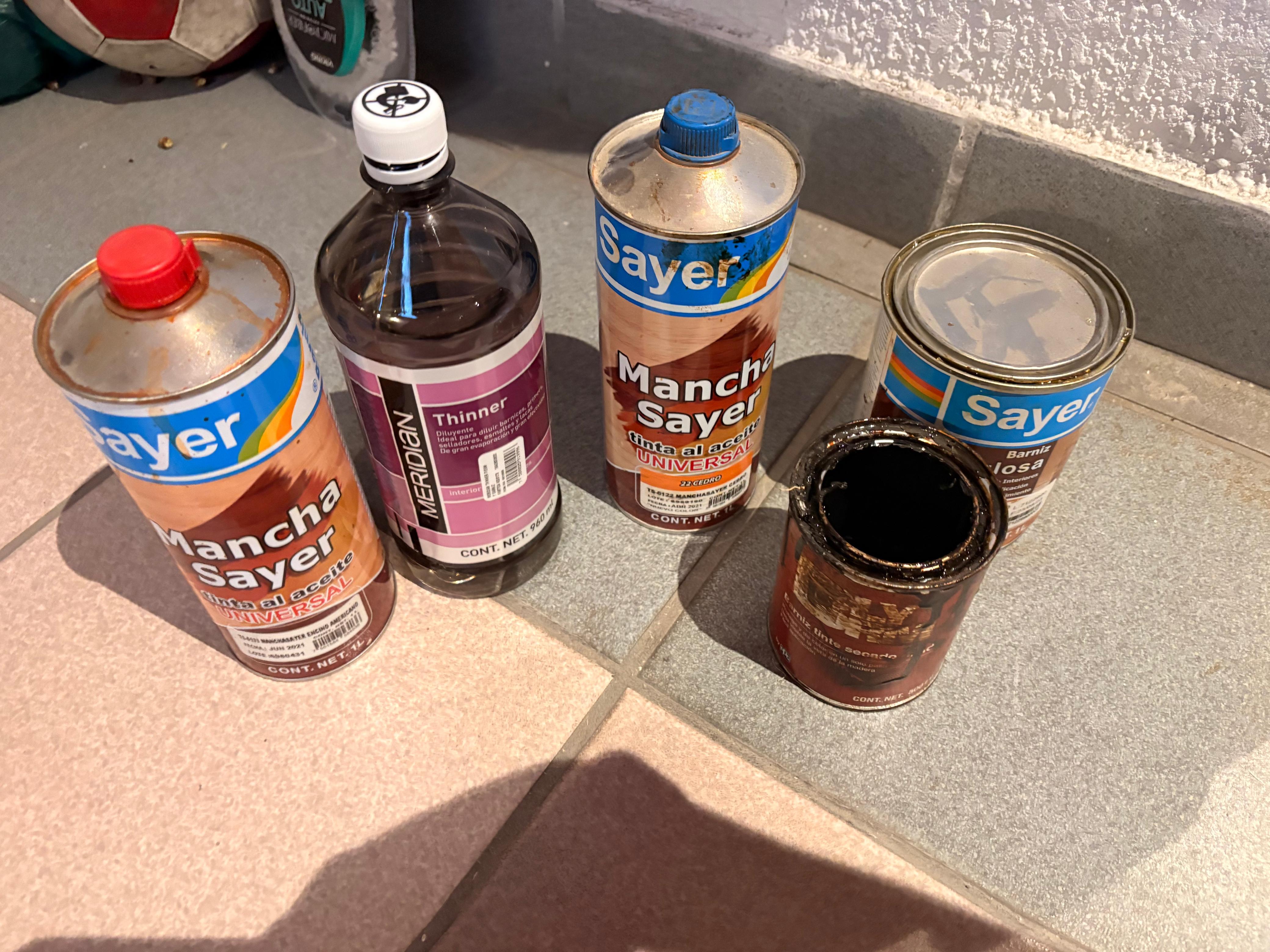
3. Then we need to gather all the paintings we need to get the right color. I also got some thiner to dilute the paint.
Materials.
1. Sayer American oak - oil-based paint
2. Sayer Cedar - oil-based paint
3. Sayer Nitrocellulose - Used for varnishing
4. Thinner - Dilute painting
5. Dark Wood varnish
Painting
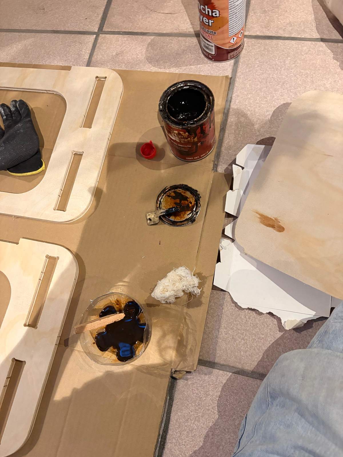
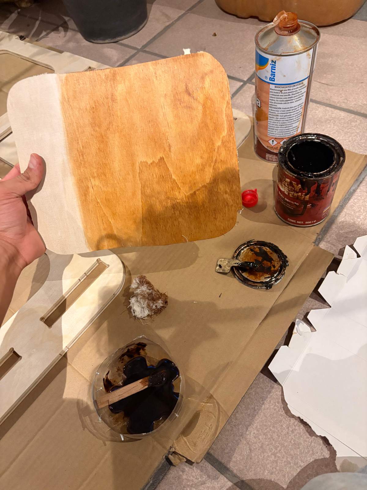
4. After that we need to mix the color to get the desired result and, once obtained the desired color, we need to give from 2 to 4 hands to our pieces to achieve a good result. The paint ratios depend on the desired result. In my case, I used approximately 40% American Oak, 30% cedar, 20% dark wood, and 10% thinner.
Painting
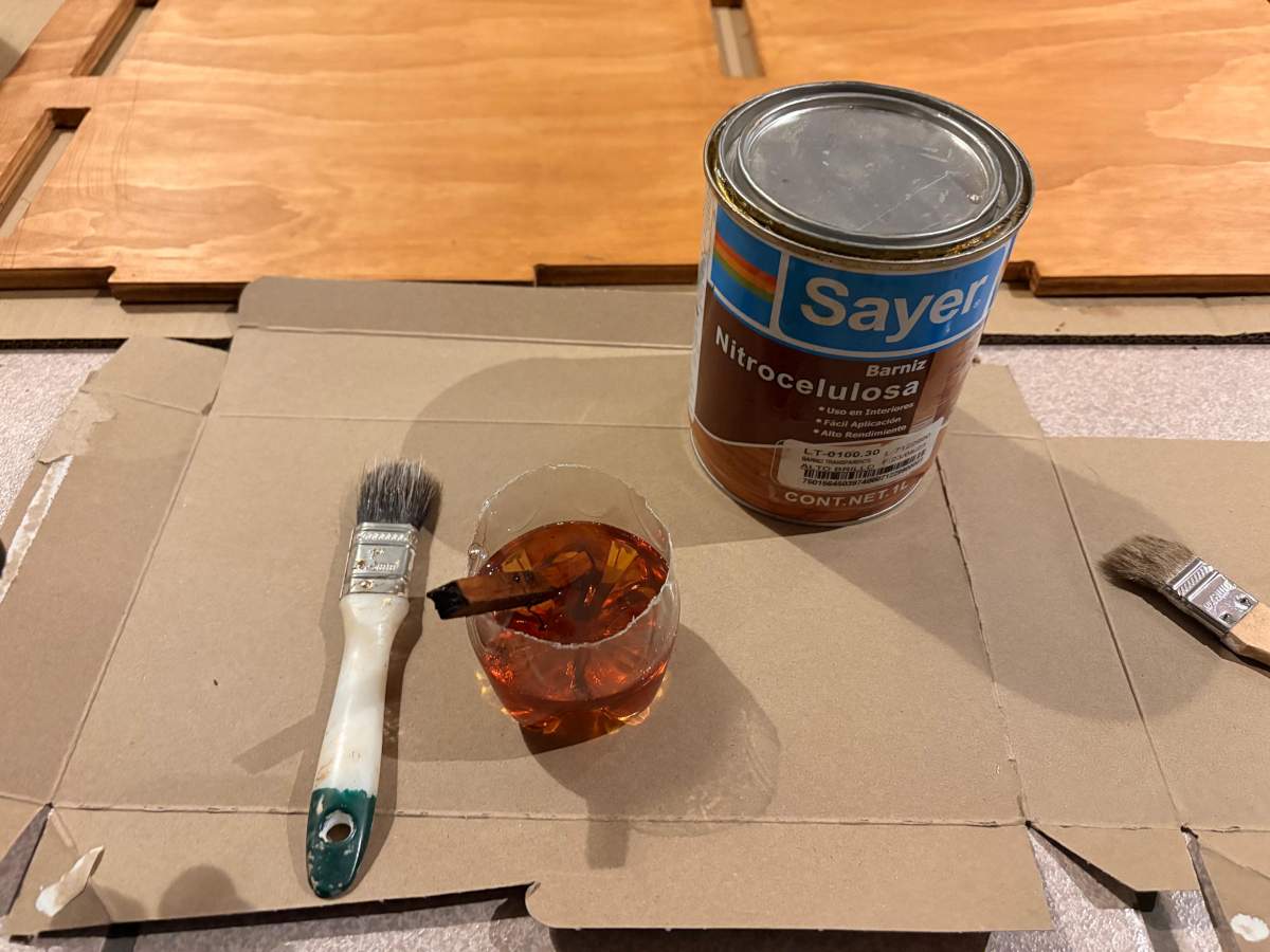
5. Finally, we have to apply the Nitrocellulose on our pieces. To use the Nitrocellulose we first have to delute it with thinner, approx. 10% thinner by volume. It is recommend to give 2 or 3 hand per piece, leaving a 60 minutes gap between each one.
Assembly
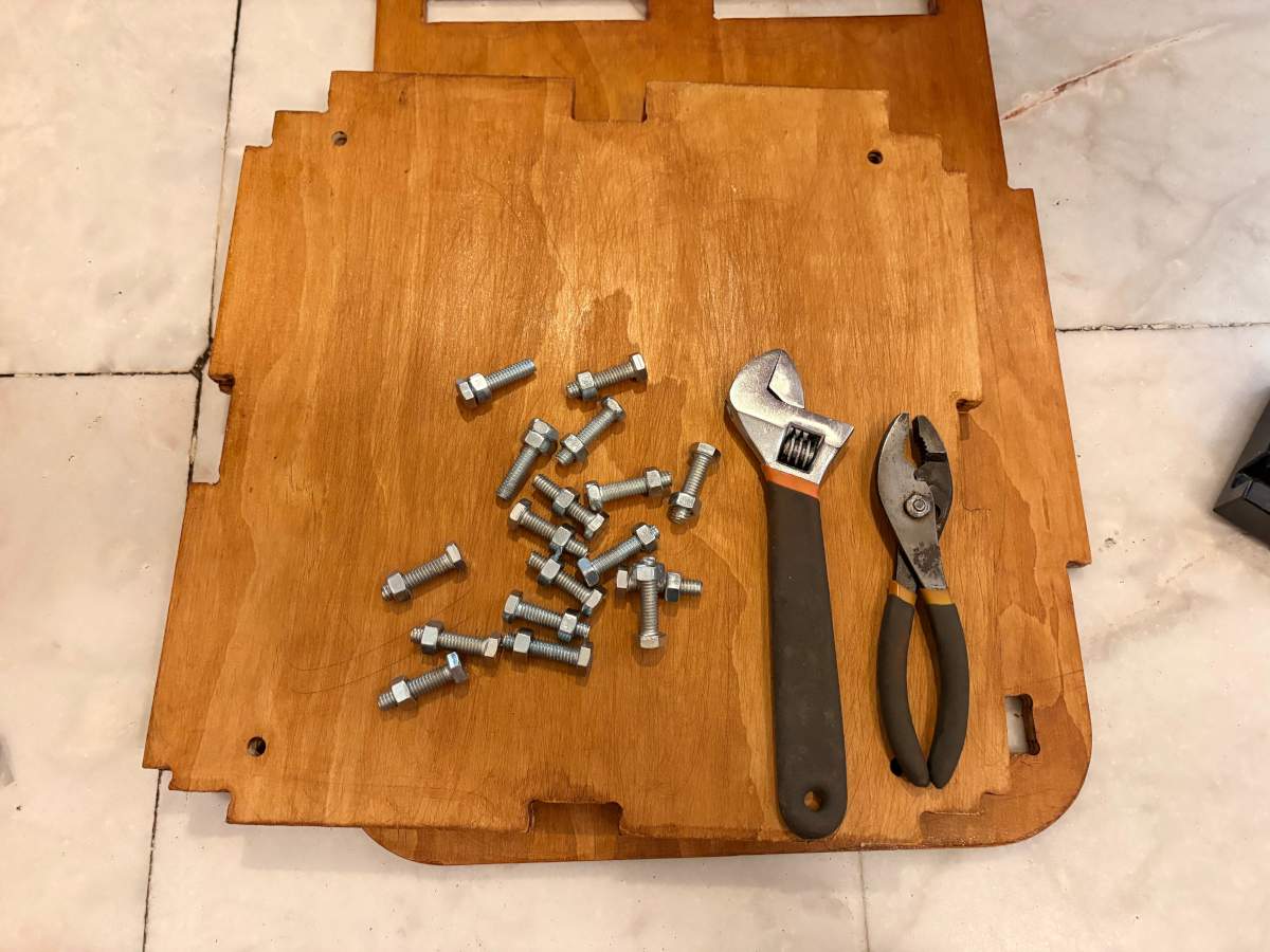
1. Once all the parts have been painted the desired color, the inner walls and the top should be secured with M8 screws, for which space has already been provided in the design.
Materials.
1. M8 screws.
2. M8 nut.
Assembly
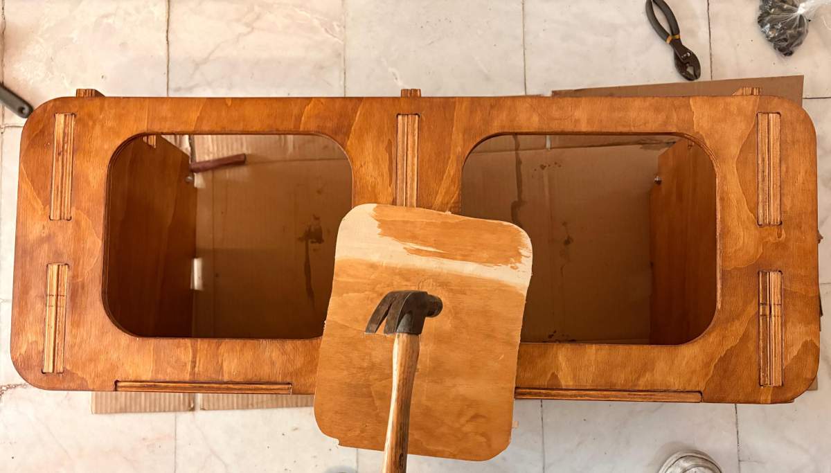
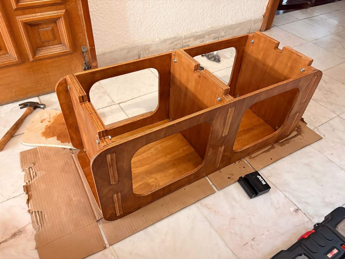
2. Because the parts are manufactured with very tight tolerances, some force is required during assembly to properly fit them together. To avoid damaging the pieces, a scrap piece of wood can be placed between the hammer and the part. This allows the wood to absorb the direct impact while still transmitting enough force to assemble the components correctly.
Assembly
3. Finally, it is important to be carefull while placing the top part, because it has to fit in three different section. My recommendation is to fit each piece in gradually, working on them all at the same time until the wood is securely in place. The reason for this is to avoid damaging the pieces; when I was putting it together, I had to use a lot of force and almost damaged an interior wall.
Results
Learning outcomes
This week, I learned many new concepts related to furniture manufacturing and design. One of the most important things I learned was how to determine the appropriate material thickness needed to prevent deformation or warping. This is achieved by applying deflection and stress analysis formulas, which help ensure that the structure is strong and stable enough to support the required loads. Understanding these calculations gave me a better appreciation of the engineering principles involved in furniture design.
I also improved my skills using Mach3 and VCarve. While working with these programs, I learned how useful features such as dogbones and automatic tolerance calculations can be during the machining process. These tools make assembly easier and improve the precision of the final parts, especially when working with CNC-manufactured components.
Another aspect I really enjoyed was working with paint and finishing techniques. I particularly like using oil-based paints because they provide very good results and enhance the natural appearance of the wood grain. The finish gives the furniture a more professional and aesthetically pleasing look while also protecting the material.
Overall, I am very satisfied with the outcome of my project. The piece of furniture turned out exactly as I intended, since it successfully functions both as a workout bench and as a small stool. Combining practicality, strength, and aesthetics into a single piece made the project very rewarding.