Week 6. Electronics design
Summary
This week we focused on learning how to design our own PCB following electrical rules, the use of different components and how to use KiCad software for making the PCBs.
Group assignment
Here is the group assignment to check more information about the topic electronics design.
1. Basic concepts
1.1 What is a PCB?
A PCB (Printed Circuit Board) is a board, usually made of insulating material, on which electronic components are placed and connected using conductive copper traces. These traces replace traditional wires and allow electrical signals and power to flow between the different components of the circuit.
1.1.1 Why is it useful?
They serve as mechanical support and a means of electrical connection, and are used in virtually all electronic devices, from computers and telephones to industrial systems.
1.1.2 Parts of the PCD and their function
- Substrate (base or dielectric material)
- Copper layers (tracks or traces)
- Pads
- Ways
- Solder Mask
- Silkscreen
- Holes
The base of the board, usually made of fiberglass and epoxy resin (FR-4), serves as mechanical support for all components and electrically isolates the copper traces.
These are the copper conductor lines etched onto the circuit board. Their function is to electrically connect the components and allow the flow of signals and power within the circuit.
These are copper areas where electronic components are soldered. They allow the components to be attached to the board and connected to the traces.
These are small, metallic holes that connect traces between different layers of the PCB. They allow signals to pass from one layer to another.
A protective layer, usually green, that covers most of the copper. Its function is to prevent short circuits, protect the copper from oxidation, and control where the solder is applied.
It is the printing of text and symbols on the circuit board. It serves to identify components, pins, values, and references, facilitating assembly and maintenance.
Perforations for through-hole components or for mechanical mounting (screws, spacers).
1.2 What is the electronic design of PCBs?
Printed circuit board (PCB) design is the process of planning and creating the physical board on which the electronic components of a circuit are mounted and connected. This process includes creating the electrical schematic, which defines the connections between components, and the PCB layout, where the components are placed on the board and the copper traces that allow the flow of signals and power between them are designed. The goal is to obtain a functional, efficient, and manufacturable board, considering aspects such as size, component placement, electrical interference, heat dissipation, and compatibility with the manufacturing process.
1.3 Ohm law
Relationship between voltage, current, and resistance in an electrical circuit. It indicates that the current flowing through a conductor is proportional to the applied voltage and inversely proportional to the resistance.
1.4 What is KiCad?
KiCad is a open-source electronic design program used to create printed circuit boards (PCBs). It can be used to draw electronic schematics, design the PCB layout where the components are placed, generate manufacturing files (such as Gerber files) for sending the board to production and visualize the design in 3D before manufacturing.
For this week assignment I will use KiCad.
1.4.1 Other softwares
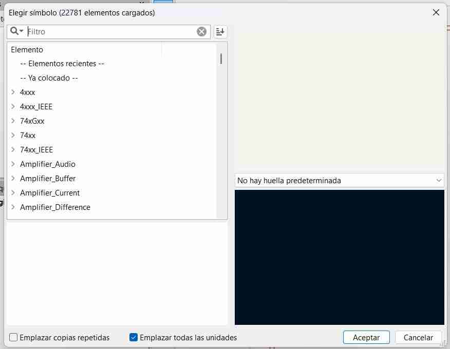
2. How to use KiCad
KiCad manages 3 types of files:
- PCB: Stores the physical PCB design, including component placement, traces, layers, and board outline for manufacturing.
- SCH: Specifies how we want our circuit to be connected.
- SPICE: Is a simulator for all electronics, and almost all electronics design programs allow simulation using this type of file.
2.1 Download and install KiCad
First we will download their website, here is the link to go directly to KiCad download website.
2.2 Install the FabAcademy library
FabAcademy has its own library in which they include most of the components we will use, so we will install that library so we can use the components with his footprints and data to make some calculus and make the pcb.
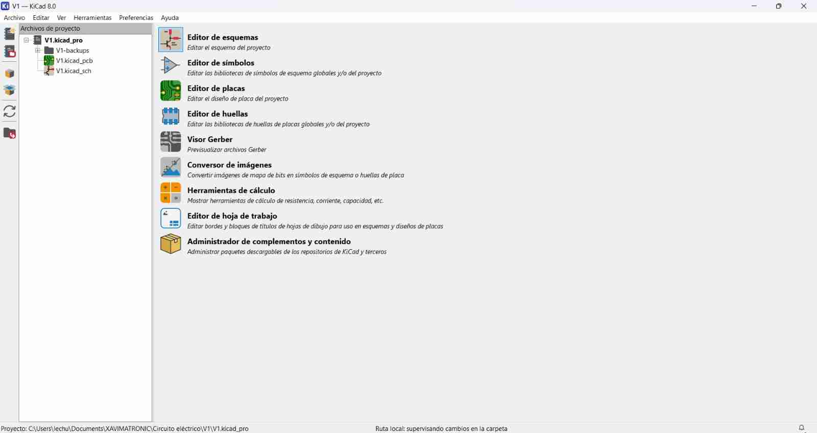
This is the main menu of KiCad.
To add this library or others, we will select the "Plugin and Content Manager" box icon. Then we select the libraries option and search for Fablib.
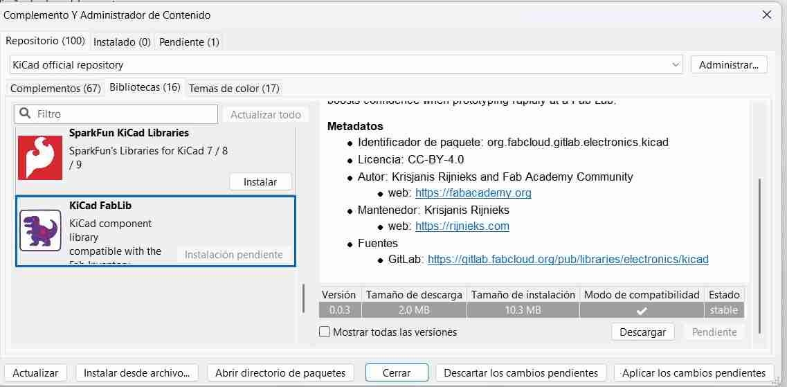
We install it and click on apply pending changes.
2.3 Create a folder for a new project
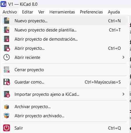
When creating a PCB, it consists of different files, so you need to create a folder for each PCB. To do this, go to File, New Project, which will create your folder to store the files.
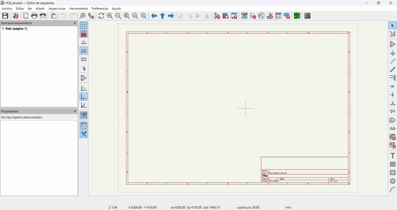
Once our project is created, we will open the sch file
2.4 Working on the schematic file
This is the first screen that greets us.
All our tools on the right side allow us to insert components into my drawing. The most important one is the triangle because it allows us to insert the components.
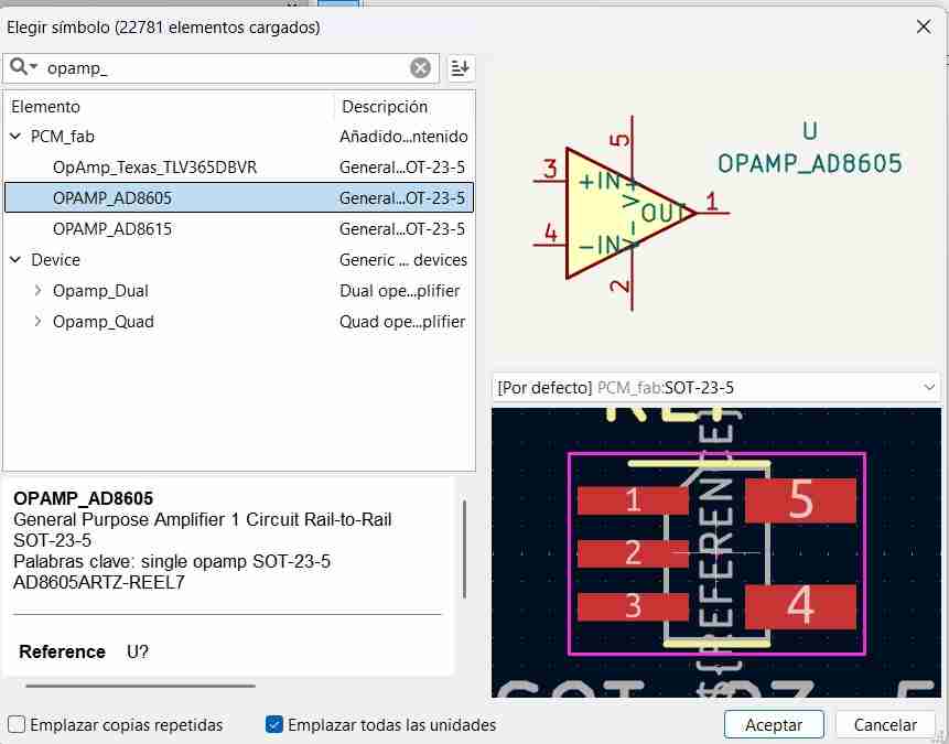
Here we see our components; you just have to select them with a click.
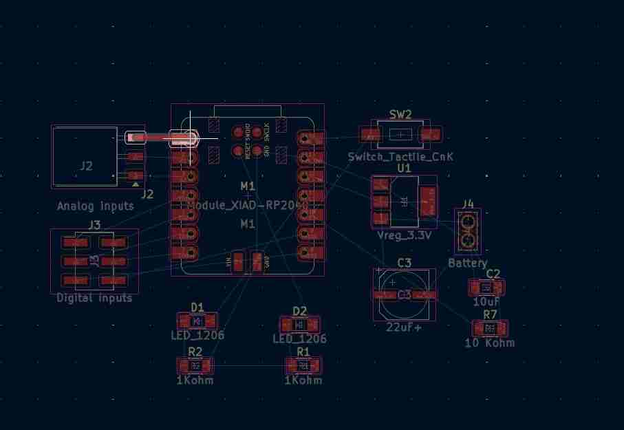
The schematic shows us a drawing of the component with its pins, and the PCB shows us the footprint that our component will have (physically), we can change the type of footprint according to our needs.
2.4.1 Footprints
The footprints can start with D or Pmeans "Through hole"; these are components that pass through the board. S means components that are soldered on top.
To find the size, we can use the numbering of our component, ordered by width x height. Then we just need to check the scale, whether it's metric or imperial.
2.4.2 Connecting components
Fow wiring we can click on the end or tip of the component that we are using, as well as we can press W and we will start drawing a cable.
We can also use labels to connect the outputs and inputs; they simply need to have the same name, and when we switch to the PCB view, they will appear connected.
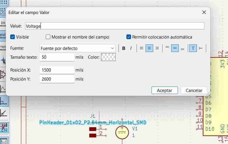
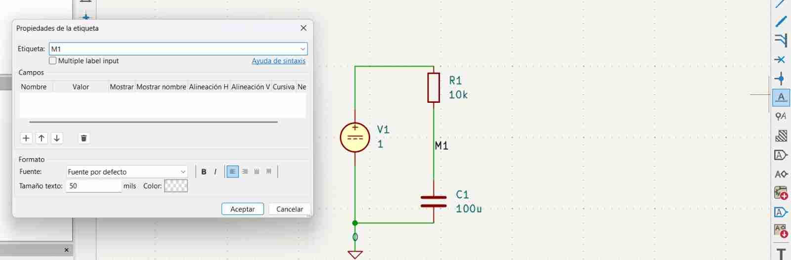
If we want to modify the name of a component, we double-click and change it.
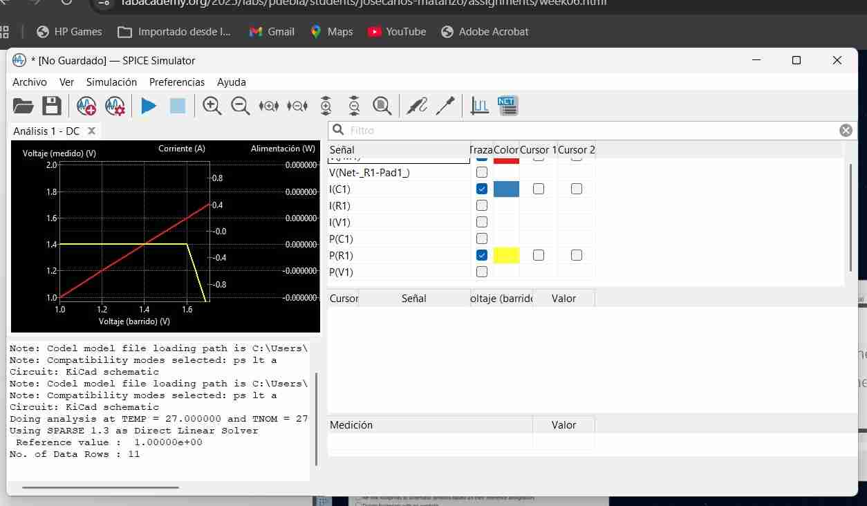
2.4.3 How the simulation works
Spice elements must be inserted to perform the simulation. This elemnents are almost all components that we have on KiCad.
I will place a small circuit to simulate it.
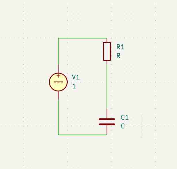
For any simulation, it's important to establish a zero reference point to determine how the measurement is being taken; this will normally be connected to the negative voltage terminal.
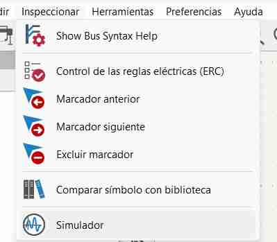
To simulate, go to the inspect tab, simulator and play.
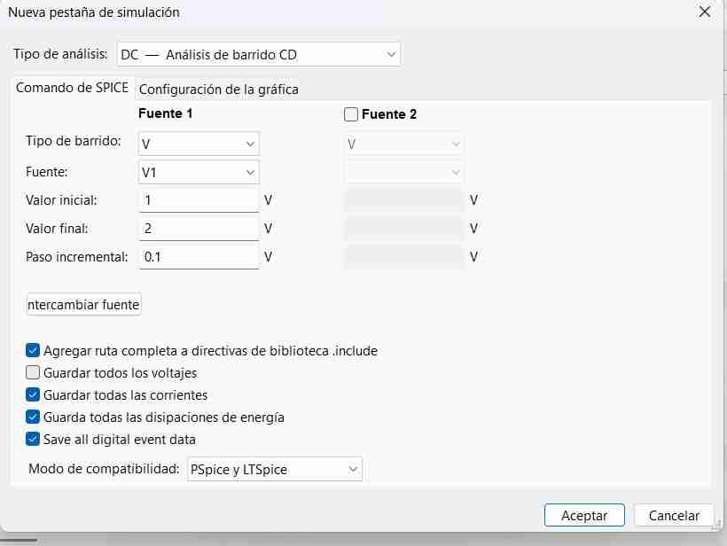
They ask us what type of DC operation we will use in this case, but we can use any type; it will depend on what each person needs.
After configuring the voltage, we go to the schematic probe tool and click. With this tool, we can measure current and voltage anywhere in the circuit over time.
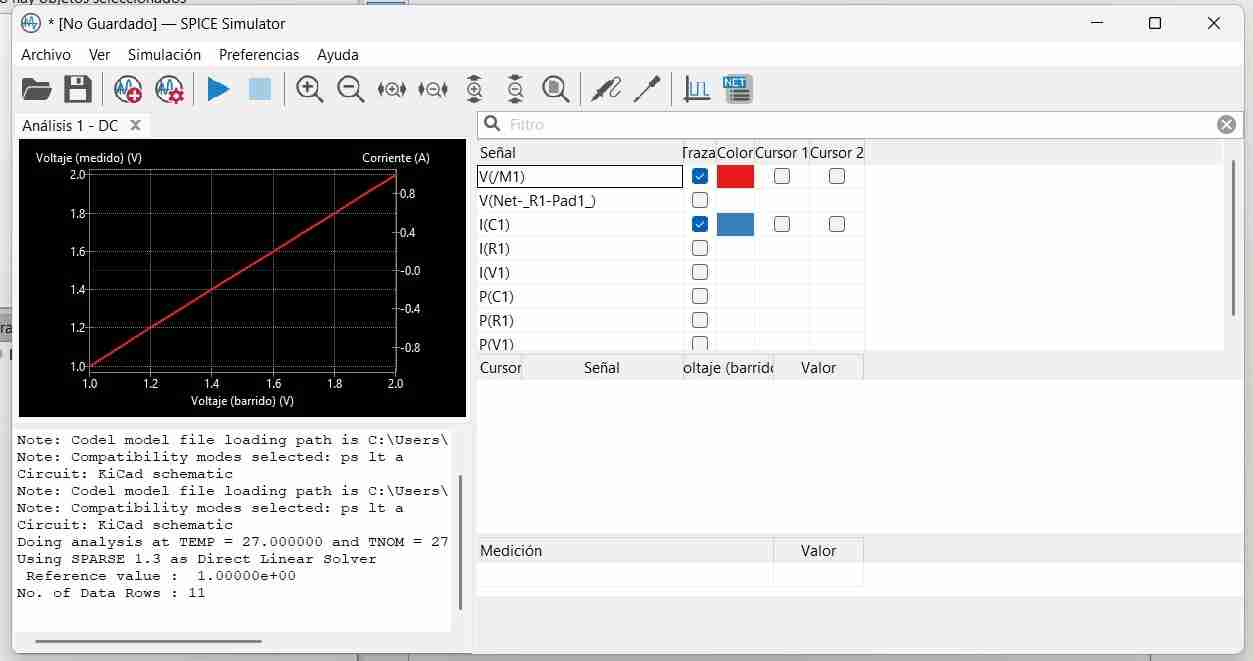
By activating or deactivating options we can see the values and their graph of other unknowns.
2.4.4 Connecting the components
If we don't know how to use a component, we can use the e command or double-click the component to open a datasheet that will show us its functions and typical applications.
In my case I use labels to connect the outputs and inputs of the Xiaomi pins.
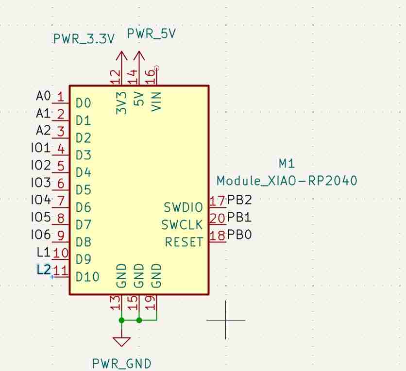
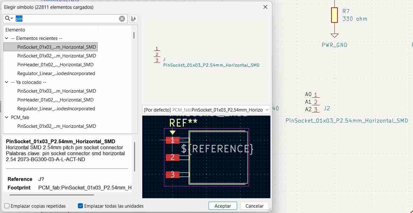
I used pin socket for analog inputs
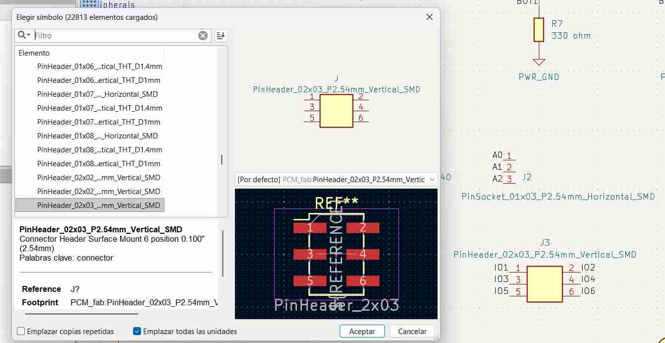
Pin header for digital inputs.
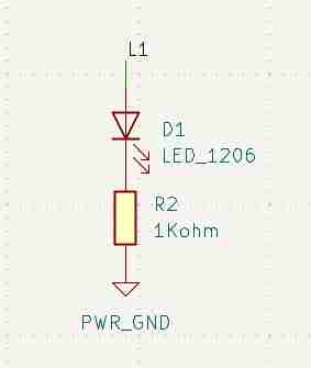
2.4.4.1 Create LED system
I will use surface mount components as they are the most suitable for PCBs. To maintain a balance between compactness and easy handling, we will be working with 1206 components, which are 3.20 x 1.60 mm.
The value that I chose for the resistor which after the LED was 1kΩ, this will limit the current to 1.3mA, which will keep the LED visible and maintainin power efficiency, while preventing the LED from burning from an excess of current.
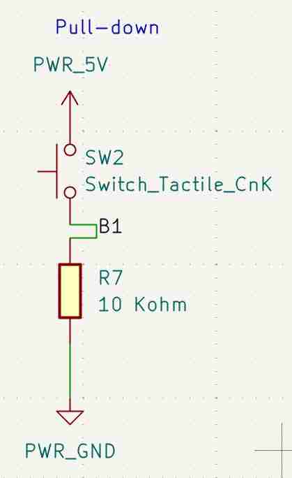
2.4.4.2 Create button system
We will make a button in a pull-down configuration, which means that the default state of the input will be false. We insert the button, the resistor, the label, power and ground. We wire the power to the button and place the label on the other side, we then continue to the resistor and end at ground. The vaule that I chose for the pull-down reistor was 10kΩ, which is a standard value used in digital electronics because it pulls the pin LOW reliably without wasting power, ensuring stable, low power operation when the button is not pressed.
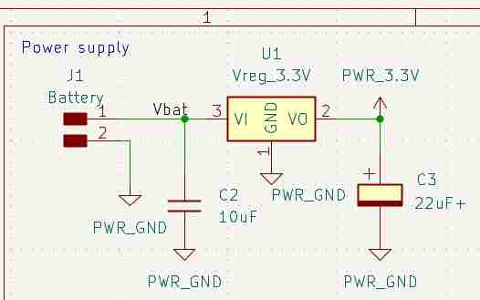
2.4.4.3 Create the voltage regulator
Will recieve electrical signals and turn them into 3.3V signals. If we don't know how to integrate them we can look for the datasheet of the component, and copy the intended applications. From the intended applications, we can copy the components and wiring that the system requires, which is precisely what we did to integrate the system into our schematic. The regulators output voltage is 3.3V, which is the voltage that the XIAO uses to operate, the value of the capacitors is of 10µF on the input side and 22µF on the output side. The input capacitor reduces voltage ripples from the power source and helps smooth sudden changes in current draw. The output capacitor keeps the 3.3V line stable when the circuit's current demand changes and prevents oscillations in the voltage regulator. The 10µF and 22µF values are recommended in most regulator datasheets, since larger caps handle power fluctuations better than smaller ones such as lµF, but too much capacitance can slow down response time, so 10µF and 22µF are a good balance.
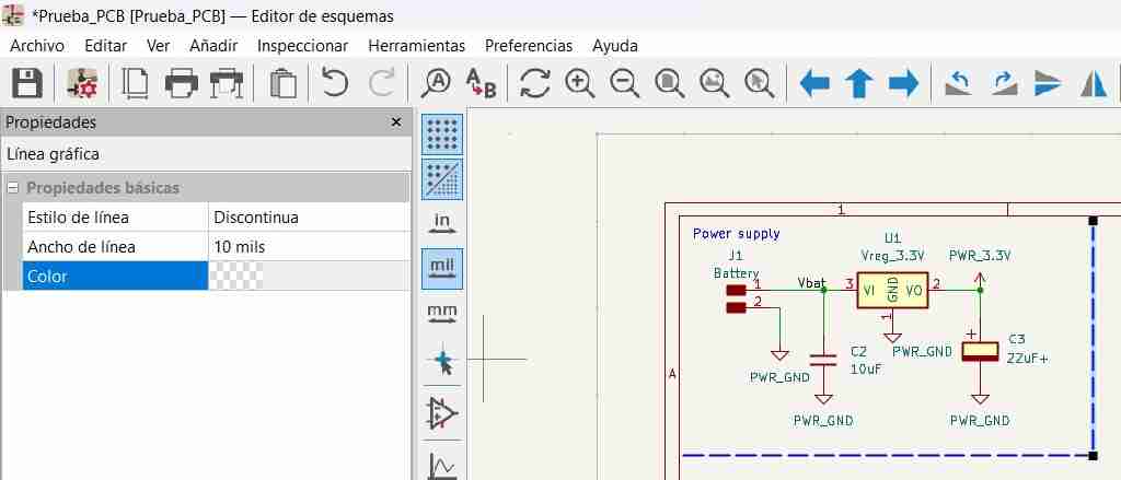
2.4.5 Add lines
We can add lines to our schematic to be better organized; these will not be visible on the PCB and are purely decorative. To do this, we press the I key and it will activate automatically.
We can change the style of the lines with a double click.
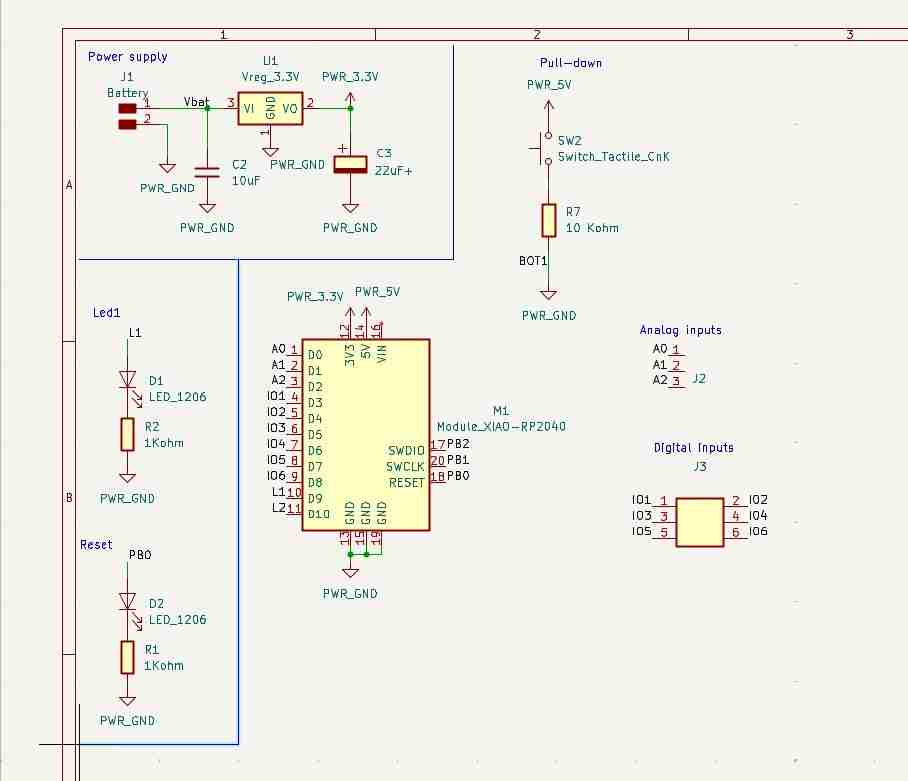
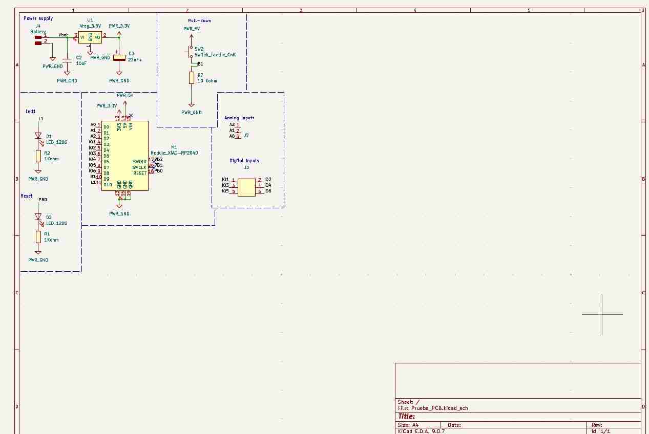
This is how our final area looks like
2.4.6 Electrical Rules Checker
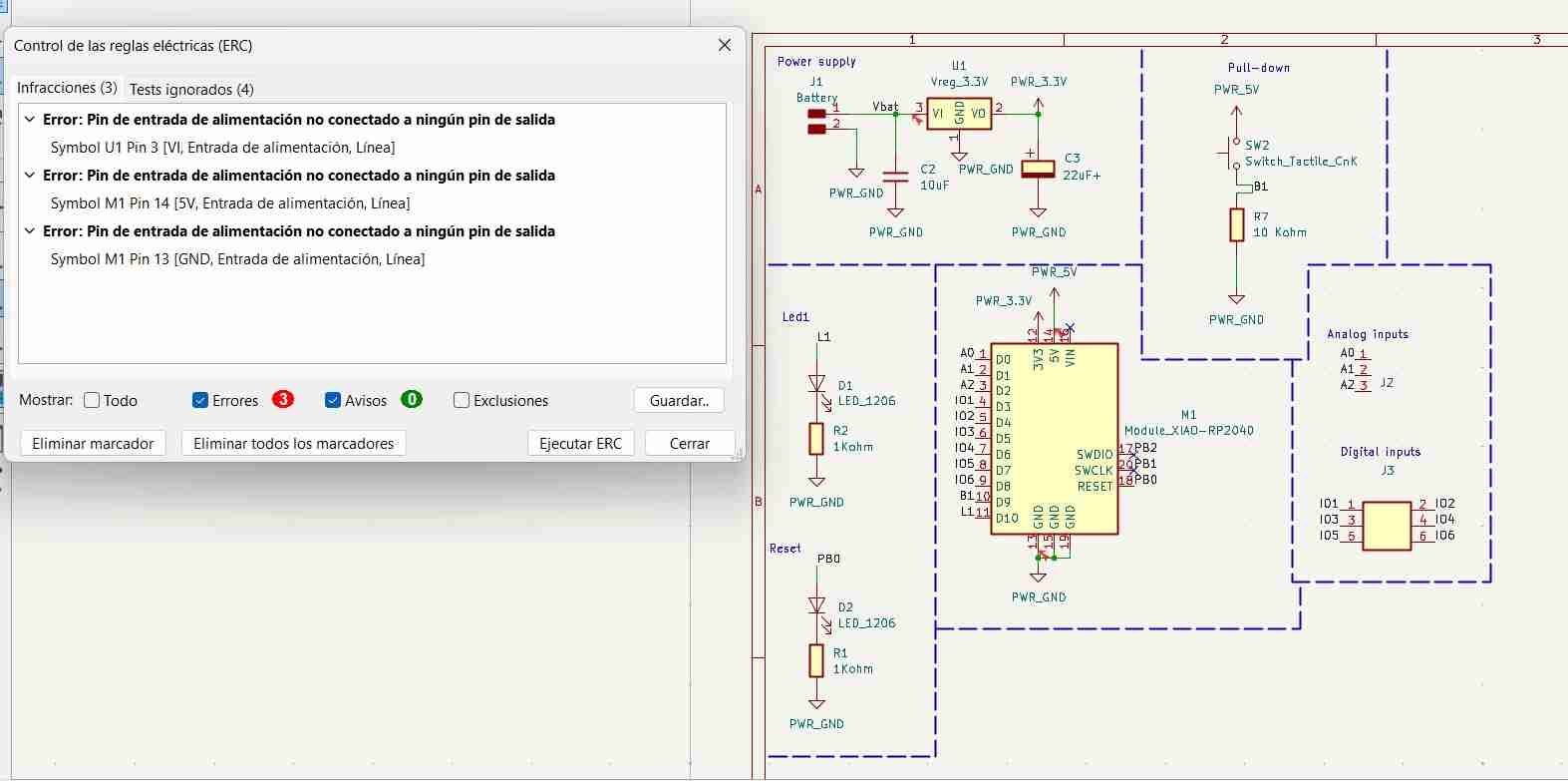
Once we are finished with the schematic, we have to use the Electrical Rules Checker or ERC to check for any errors in our design. It is located in the toolbar at the top.
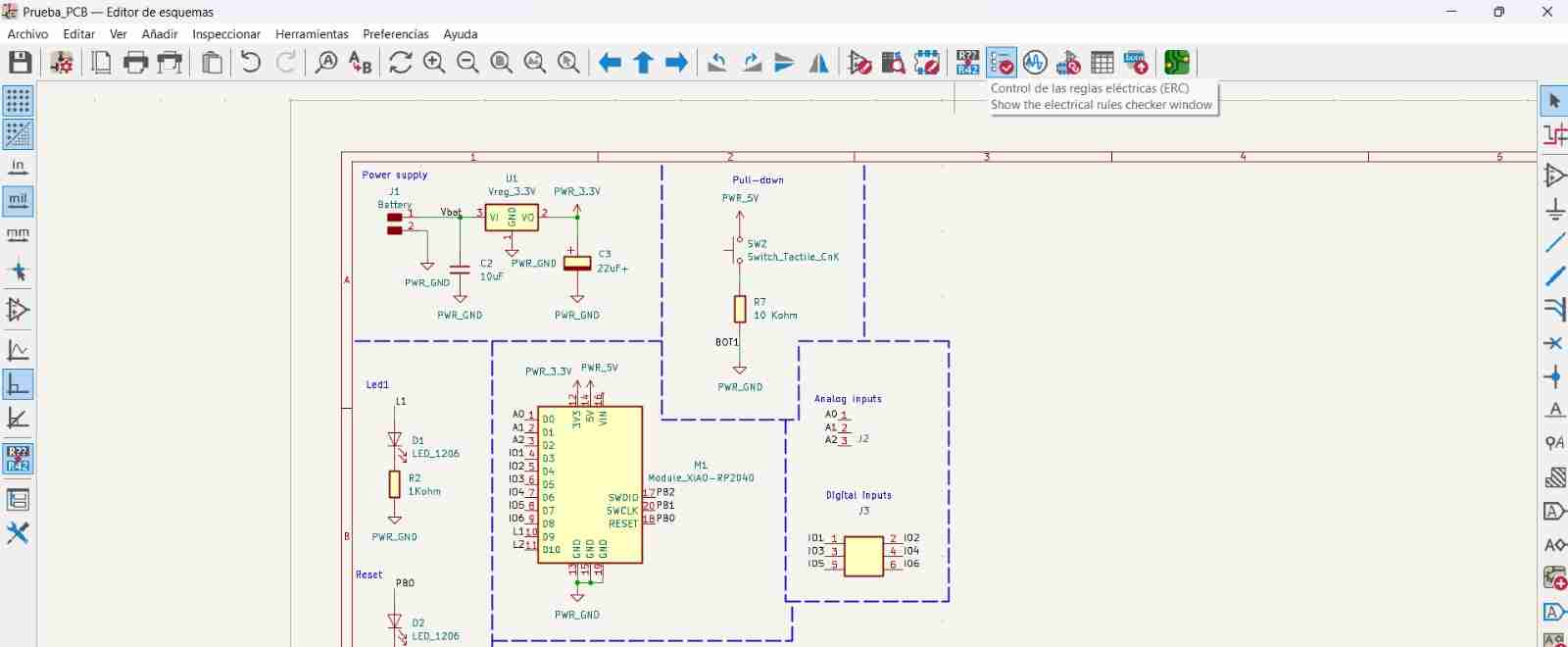
We then run the ERC, which will display all possible errors in our schematic.
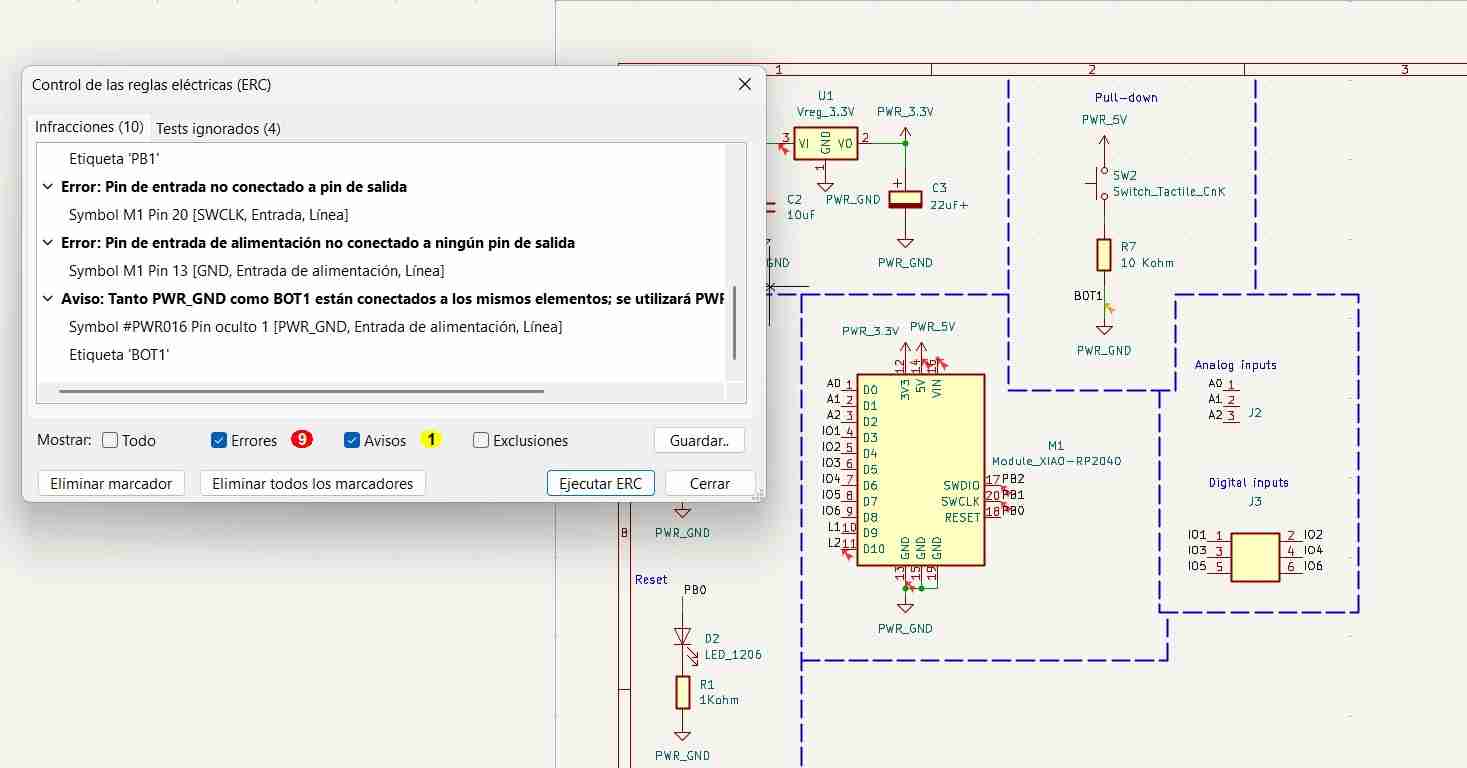
Any unused pins will be classified as an error, delete this we will use the place no connect flags tools, denoted by a line and a cross. We will place one of these crosses on any unused pins. When we run the ERC again, these errors will disappear
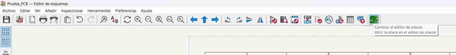
2.5 Working on the PCB file
Let's click on the PCB button (the green one)
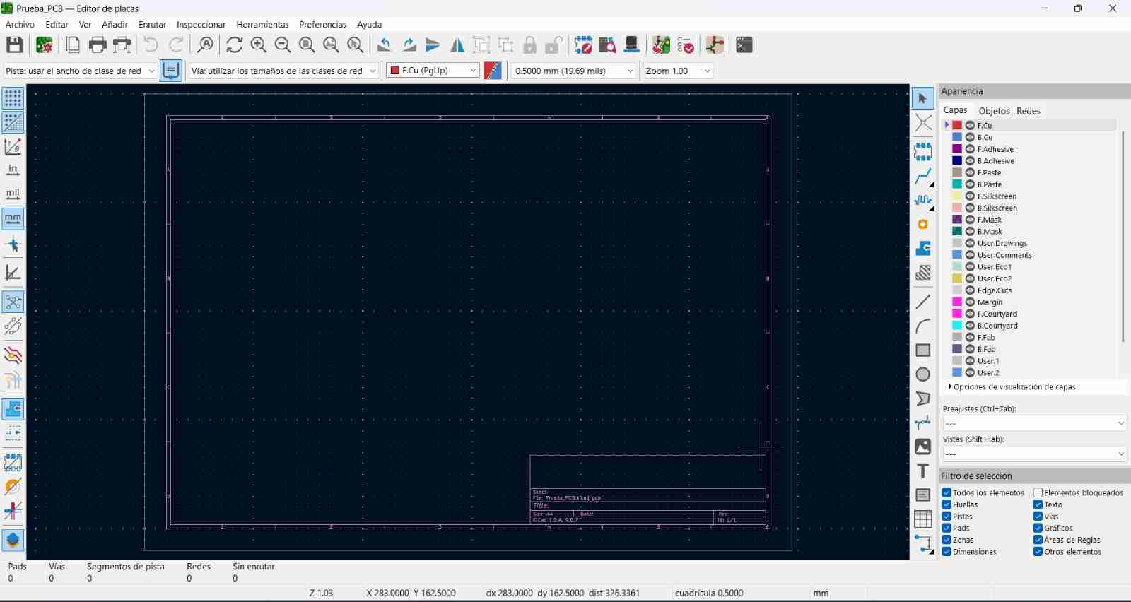
This is the screen that welcomes us
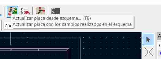
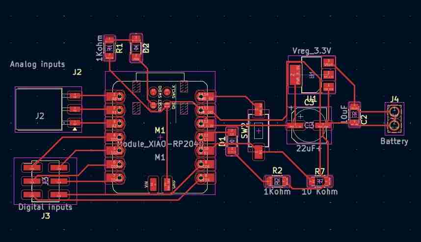
Once we are in the PCB layout editor, we have to update the PCB from the schematic. We do this by clicking on the icon with half a schematic and half a PCB on the top tool bar of the screen and then on the update PCB button, this will import all of the components present on the schematic.
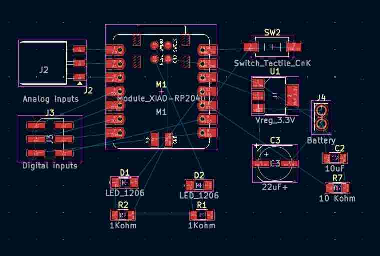
The program inserts the components together and disconnected; we can arrange them as needed.
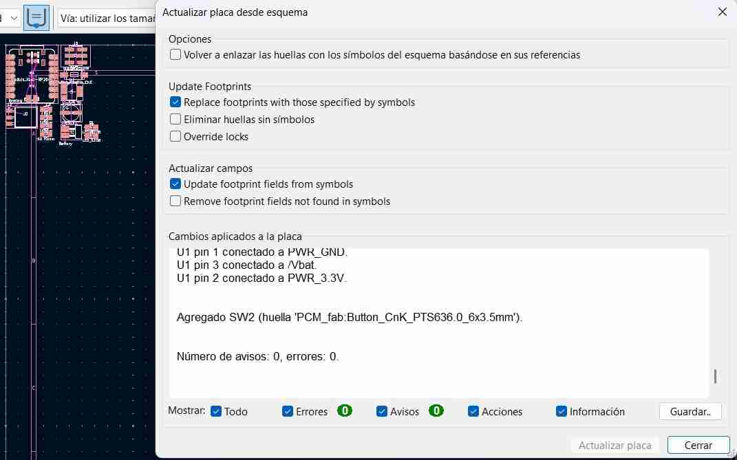
This is how it looks like
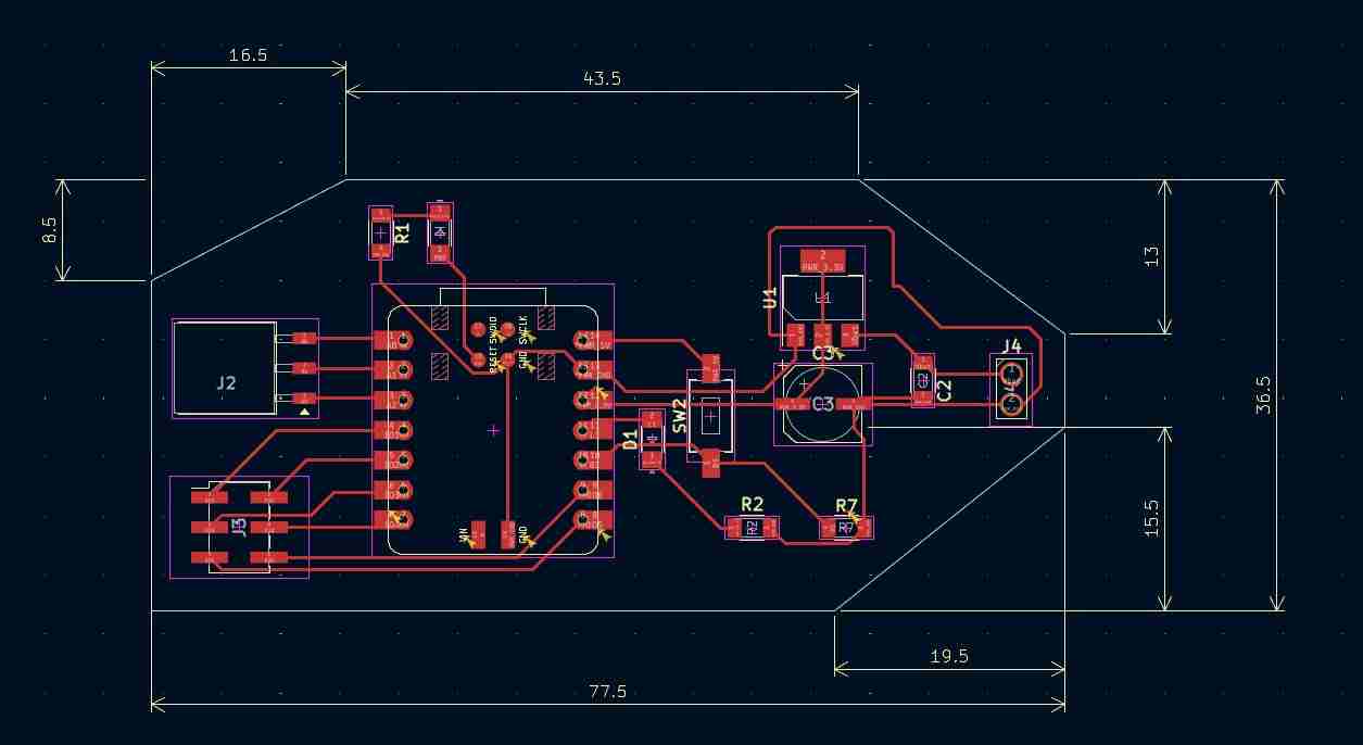
2.5.1 Calculate the width of our track and modifying them
Before wire the components together, we need to calculate the width of our trace. This is important because if the width is too small, it can affect the current flow, voltage drop, heat dissipation, or signal integrity (in fast signals).
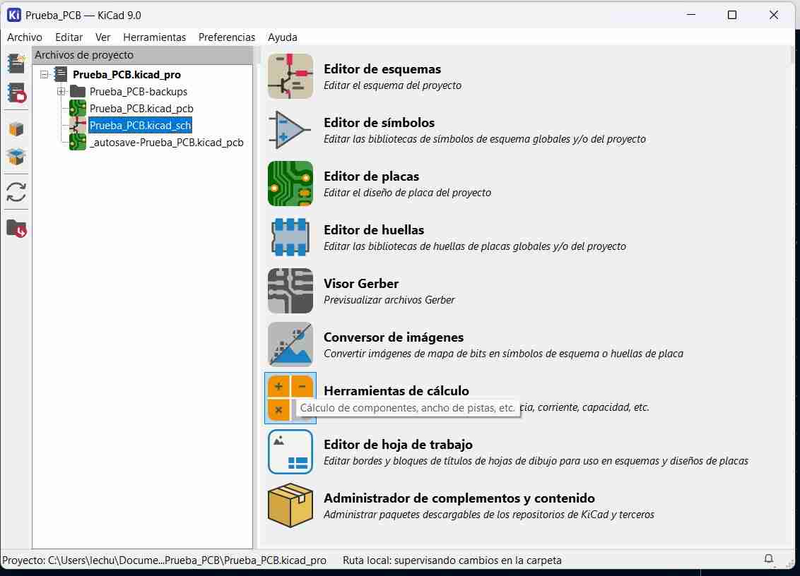
To do this, we will open the calculator tool from the main menu.
Once open, we click on "Electrical spacing" and we can see which width is best for us to use.
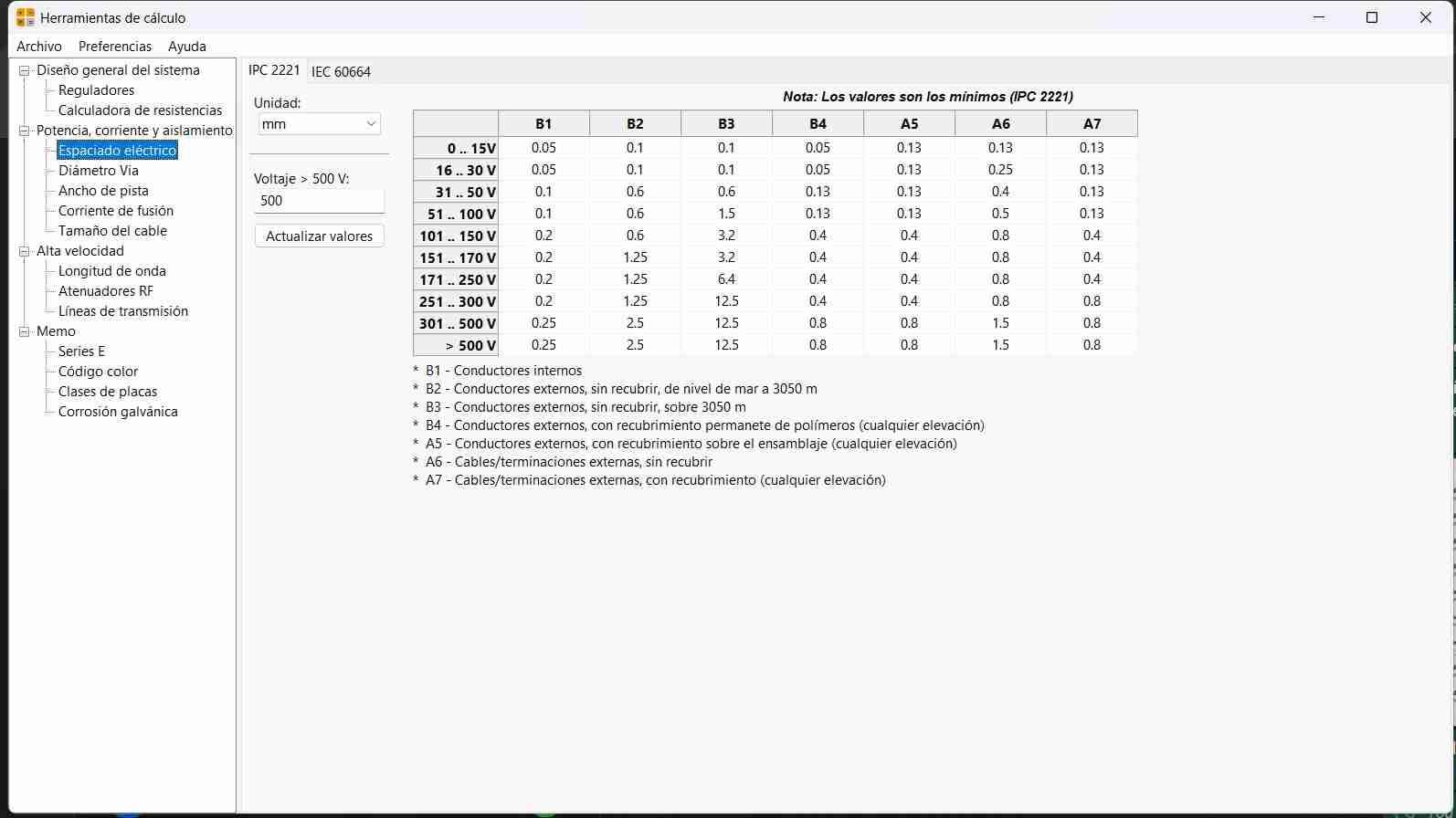
I will use the size of part B2 since my voltage will not be greater than 5. Then in "Track width" I write the maximum current and temperature values that I expect, obtaining that my track width should be 0.3 mm.
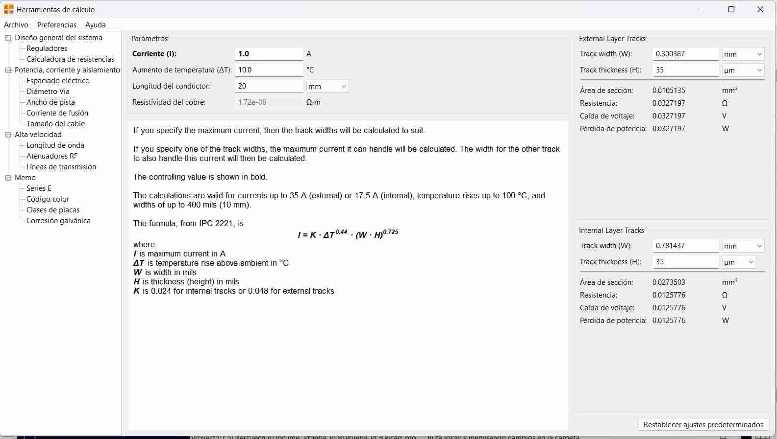
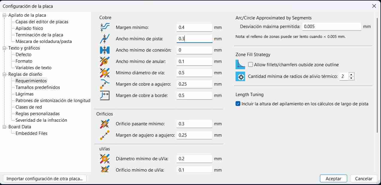
We return to the PCB layout and configure the track width and we click on the board settings button
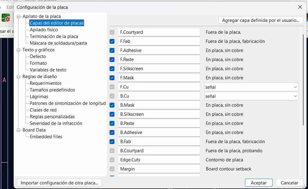
In the Requirements tab, we modify our track width and click OK.
2.5.2 Wiring the components
We have a button called "route" which, when selected, allows us to connect components. To connect them, you have to select the red side of one and the other side where it connects.
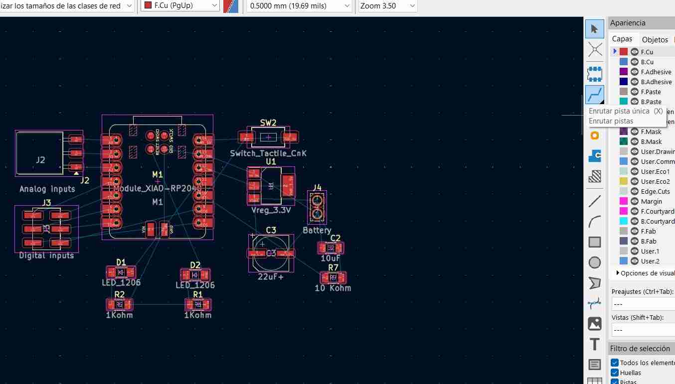
KiCad itself helps us to do this tracing by making only this visible.
This is what our components look like once connected.
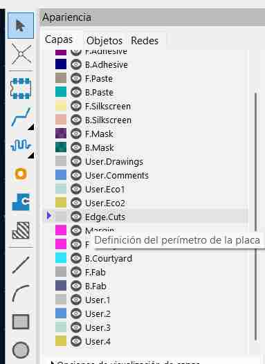
2.5.3 Place cutting edges
We draw the borders with the Draw lines tool. To define the cuts on our PCB, we go to the layers tab and select edge.cut.
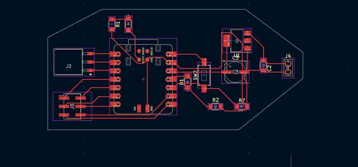
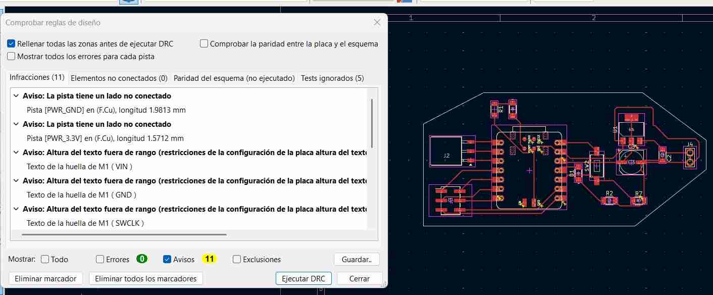
2.5.4 Design rules
We can do something similar to the ERC; DRC will tell us these possible errors. These warnings are related to text and the Silkscreen, so I can ignore them.
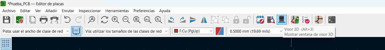
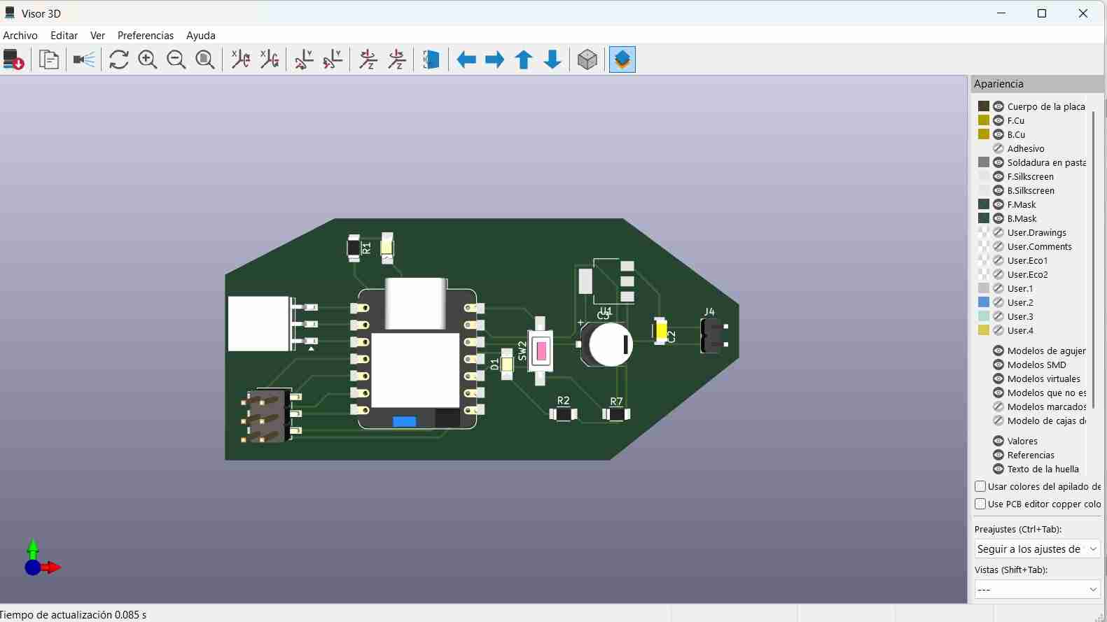
2.6 3D view
With the 3D Viewer tool we can see the 3D model of our PCB, we just have to click on it.
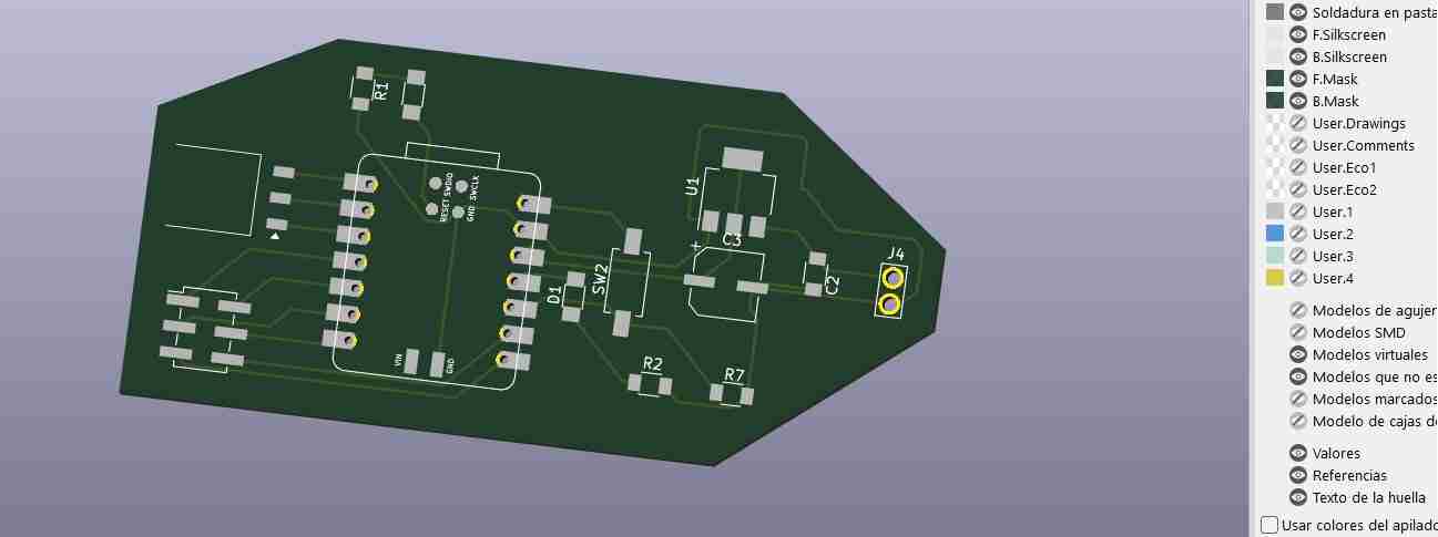
This is how my 3D model of the PCB look like.
To get this view without components, we deactivated SMD Models and hole model.
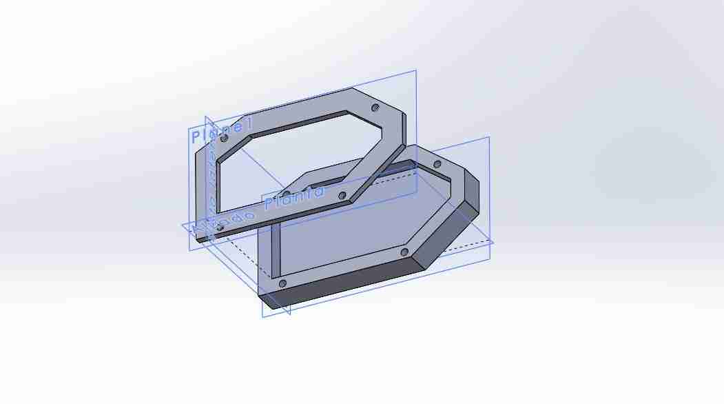
3. Designing the case for our PCB
We take measurements using the Draw orthogonal dimensions tool.
Now we will open SolidWorks to sedign the case with the measurements that we just took. We create an sketch and put the measures.
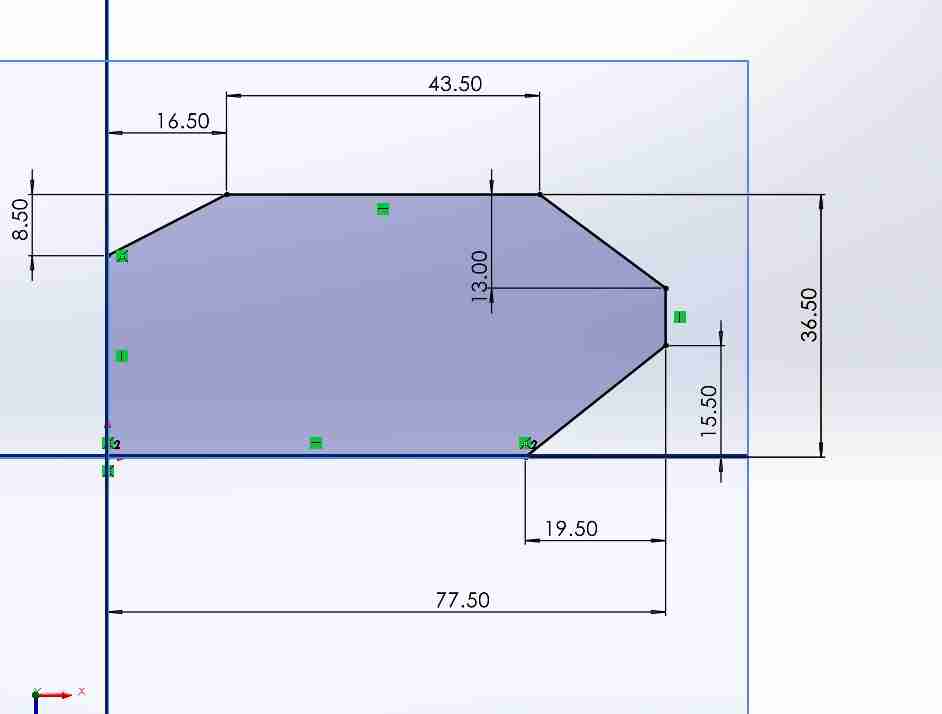
After extruding in a new sketch we make an exterior offset of the border to place the holes for the screws.
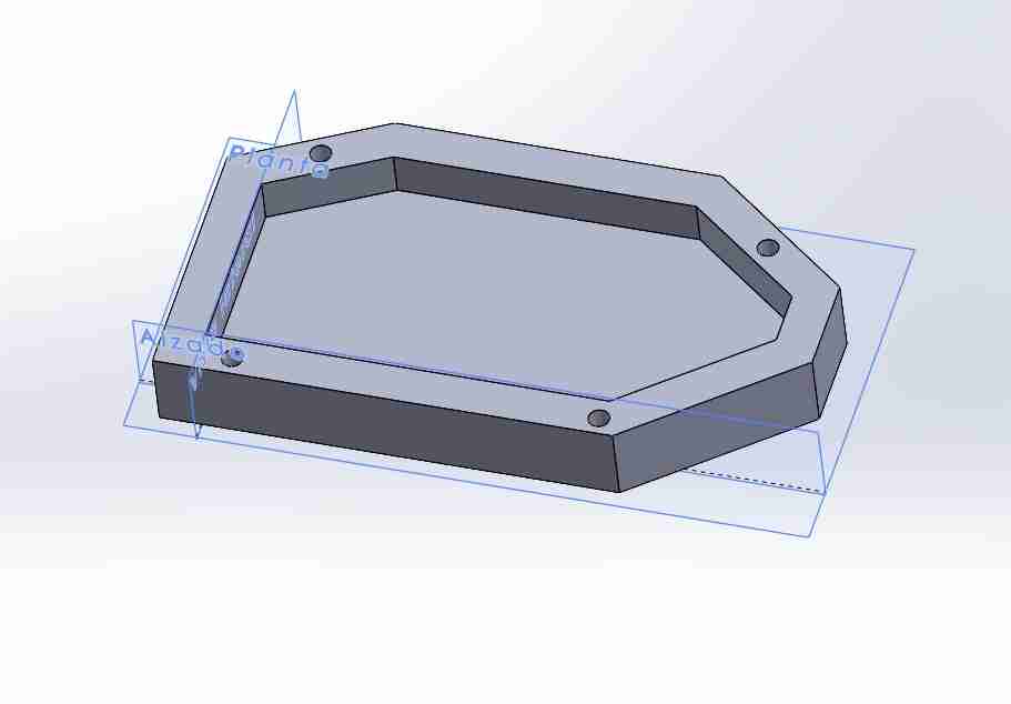
To make the lid, I will create a plane above which I will use convert entities and offset.
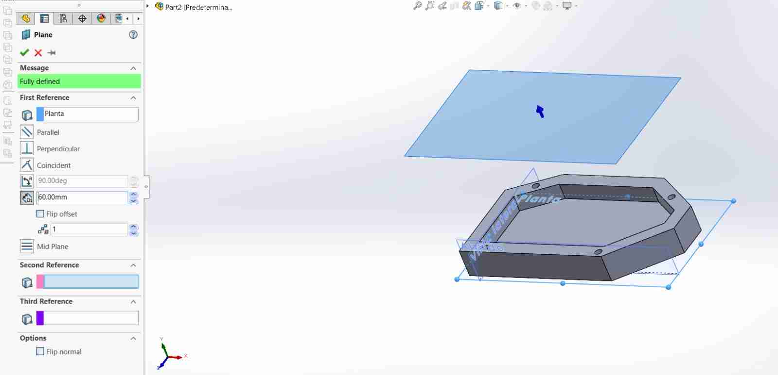
In the new plane we use convert entities for copy paste the borders of the base to make the lid, and offset to make a hole so we can see the LED and oush our button.
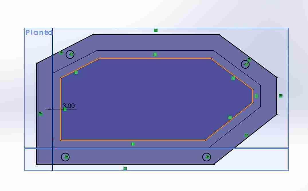
Here is the final look of the case, I designed so the holes can fit M3 screws.
4. Conclusions
In my experience, it's always best to have everything you'll use in the schematic before moving to the PCB layout, since adding new components can affect existing connections, requiring you to redraw your entire PCB design. If possible, have someone with more experience review your schematic to identify any errors or missing components.
5. Files created
Click on the "Download ZIP" to download all the files I made for this week assignment