Week 06
Electronics Design

This week we worked on understanding how circuits work, simulating the way the circuits would work and how we can build a PCB. This includes learning about the different types of components used for building the circuits.
KiCad
Personal and Group Assignment
This week’s personal assignment was to design a circuit, run a simulation and design the PCB, while document the process.
Group Assignment
Here’s the link to our group assignment of this week.
What is electronics design?
It is the engineering process of creating, developing, and integrating electronic circuits and components (like resistors, transistors, and ICs) to build functional systems.
What does it work for?
It helps us create functional, reliable, and manufacturable electronic circuits and systems for industries like consumer electronics, automotive, healthcare, and telecommunications. It transforms concepts into working prototypes by defining, simulating, and testing PCB layouts, components, and embedded systems, ensuring they meet performance, safety, and cost requirements.
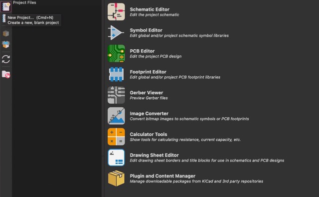
Understanding KiCad
To design the PCB for the dog wearable for my final project, I used KiCad. It is an open-source Electronic Design Automation (EDA) software. For Fab Academy, it's crucial to understand that designing a board here is not a single step, but a three-part workflow:
The Core Workflow
KiCad divides the design process into distinct environments that must be completed in order:
- Eeschema: The logical editor. Here you draw the schematic using abstract symbols (like a triangle for an LED).
- Footprint Assignment: The bridge between logic and reality. You tell KiCad that the abstract LED symbol is specifically a 5mm Through-Hole LED physically.
- Pcbnew: The physical layout editor. Here you arrange the real components and draw the copper traces.
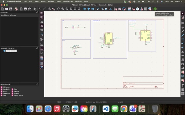
Logical Design
When designing the circuit for the XIAO RP2040 and the MPU6050, keeping the schematic readable was a priority.
Net Labels over Wires
Instead of drawing a web of messy green lines, I used Net Labels (like SDA and SCL for the I2C communication). KiCad automatically connects any pins sharing the same label.
Before moving to the PCB, I ran the ERC (Electrical Rules Checker). To avoid false errors about power sources, I added PWR_FLAG symbols to the 3.3V and GND nets, telling KiCad that the XIAO acts as our power source.
Physical Routing
In the PCB editor, the design becomes physical. I had to make strategic decisions regarding the layers and track widths:
- Track Widths: I used a standard
0.25mmwidth for data signals (like the button and IMU data), but increased the width to0.5mmfor power lines (3.3V and GND) to ensure stable current flow. - Layers: I routed the copper traces on the
F.Cu(Front Copper) layer. - Edge Cuts: Finally, I used the
Edge.Cutslayer to draw the custom board outline, giving the PCB the shape of my dog! 🐾
KiCad Shortcuts (Cheatsheet)
To work faster and more efficiently in KiCad, mastering keyboard shortcuts is essential. Here are the most useful commands I constantly used during my circuit design process:
| Key | Action | Environment |
|---|---|---|
| A | Add a symbol / Add a footprint | Schematic & PCB |
| M | Move an item (disconnects wires) | Schematic & PCB |
| G | Grab / Drag an item (keeps wires connected) | Schematic & PCB |
| R | Rotate an item 90 degrees | Schematic & PCB |
| W | Draw a Wire | Schematic |
| L | Add a Net Label | Schematic |
| P | Add Power symbol (VCC, GND) | Schematic |
| E / V | Edit properties / Edit Value | Schematic |
| X | Route a track (Draw copper line) | PCB layout |
| Del | Delete selected item | Schematic & PCB |
KiCad Guide: Dog Wearable
XIAO RP2040 + MPU-6050 · Step-by-step from scratch
Phase 1 — Setup

01. Install KiCad
Download and install KiCad 7 or later on your computer (Windows, Mac or Linux).
- ✓Install with all default libraries
- ✓Open the Project Manager to start
Tip: Always use the latest stable version for better compatibility.
02. Create a new project
Organize your files from the start to keep the schematic and PCB linked.
Go to:
File → New Project
- ✓Name it
dog_wearable - ✓Keeps .kicad_sch and .kicad_pcb together
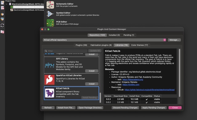
03. Manage Libraries
Add specific footprints or symbols that aren't in the default KiCad library.
Path:
Preferences → Manage Symbol Libraries
- 1Click the folder icon to add
.kicad_sym - 2Repeat in "Manage Footprint Libraries"
Phase 2 — Schematic
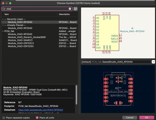
01. Add XIAO RP2040
Place the main microcontroller on the schematic canvas.
- APress A to open symbol browser
- 🔍Search for "XIAO RP2040"
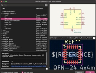
02. Add the MPU-6050
Add the motion sensor to the schematic, leaving space for wires.
Library:
Sensor_Motion
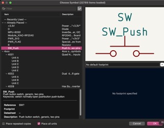
03. UI Components
Add the button, LED, and required resistors using the browser (A).
- 1
SW_Push - 2
LED
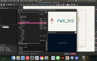
04. Power Symbols
Connect power cleanly using PWR and GND symbols.
- PPress P for power menu
- 🚩Add
PWR_FLAG
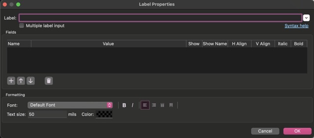
05. Use Net Labels
Instead of drawing long wires, use labels for a clean schematic.
Shortcut:
Press 'L' to Label
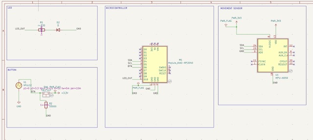
06. All Connections Via Net Labels
After connecting everything, it dshould look like this.
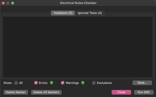
07. Run ERC
Verify there are no logical errors in your schematic.
- ✓Electrical Rules Checker
Bill of Materials & Pinout
This table describes the components used for the Dog Wearable PCB and their specific connections to the XIAO RP2040.
| Component | Qty | Connection (XIAO) | Function |
|---|---|---|---|
| XIAO RP2040 | 1 | Main Controller | The brain of the wearable. |
| MPU-6050 | 1 | D4 (SDA) / D5 (SCL) | IMU Sensor for motion detection. |
| Push Button | 1 | D6 (Input) | User interface to trigger events. |
| Red LED | 1 | D10 (Output) | Visual status indicator. |
| Resistor 330Ω | 1 | In series with LED | Current limiter for the LED. |
| Resistor 10kΩ | 1 | Connected to D6 | Pull-down resistor for the button. |
| Pin Headers | 2 | VCC / GND / Pins | To connect |
Phase 3 — PCB Layout
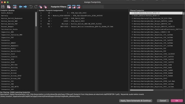
01. Assign Footprints
Link each symbol to its real physical package (Tools → Assign Footprints).
- ✓XIAO:
Seeed footprint - ✓MPU:
Module_GY-521 - ✓LED:
LED_D5.0mm
02. Open PCB Editor
Transfer your design from the schematic to the physical board using the "switch to PCB editor" button.
Keys:
G (Grab) / R (Rotate)
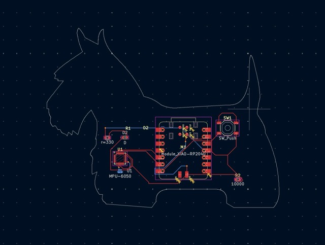
03. Edge Cuts (Dog Shape!)
Define the physical shape. I
used the Edge.Cuts layer to draw
the dog outline.
- 1Select
Edge.Cutslayer - 2Use Graphic Lines / Circles
- 3Ensure the path is closed
04. Route Tracks
Physically connect the pads. Use thicker tracks for power lines.
- XPress X to route
- ✓0.25mm for signals
- ✓0.50mm for VCC/GND
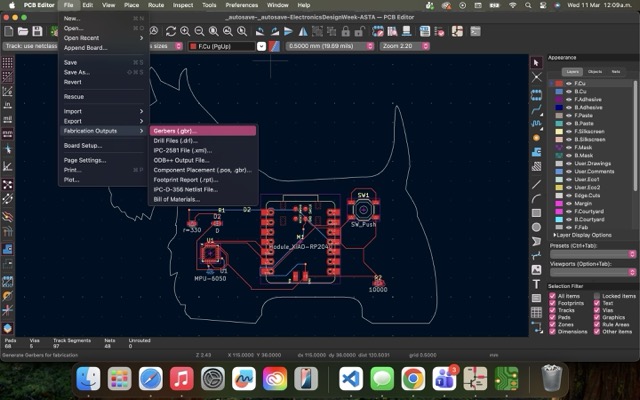
05. Export Gerbers
Final verification and files to send for fabrication.