Software
KiCad, Gerber2PNG and Modsproject
Fab Academy 2026
Designing, manufacturing and testing a custom PCB using KiCad and the MonoFab SRM-20.
KiCad, Gerber2PNG and Modsproject
Roland MonoFab SRM-20
PCB design, routing, soldering and testing
From the group assignment, I reinforced my understanding of different PCB fabrication methods by comparing mechanical milling and laser processing.
Using the SRM-20, I observed how parameters such as tool diameter, cutting depth, and feed rate directly affect the resolution and quality of the traces.
Through the clearance and width test, I learned how to determine the minimum trace width and spacing required for reliable PCB production.
Overall, this assignment helped me better understand how to choose the correct fabrication process and machine parameters to ensure successful PCB manufacturing.
Create the electronic schematic and connect the components in KiCad.
Define footprints, routing, trace widths and board dimensions.
Generate toolpaths and fabricate the PCB using the MonoFab machine.
Assemble the components and validate the functionality of the board.
The first step was downloading and installing the Fab Academy libraries for KiCad.
To download them, click here .
Add the ".pretty" file inside the footprint manager.
Add the "_sym" file inside the symbol library manager.
Configure the complete Fab Academy library folder.
After setting up the libraries, I started creating the schematic in KiCad.
Components can be added by pressing the "A" key.
Power symbols can be added by pressing the "P" key.
The Electrical Rules Check helps identify connection problems.
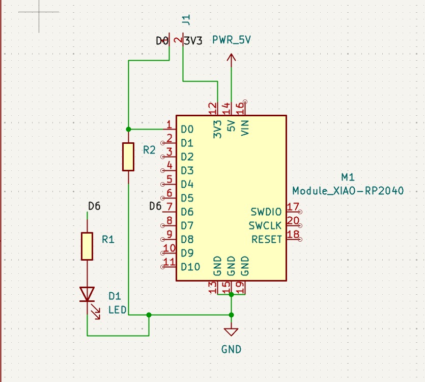
Before routing the PCB, I assigned footprints to all components and configured the design rules according to the MonoFab machine capabilities.
Minimum spacing between traces: 0.4 mm
Minimum trace width: 0.8 mm
Used to reduce the number of traces and simplify routing.
After finishing the PCB design, I exported the Gerber files and converted them into PNG images using Gerber2PNG.
Then I imported the generated files into Modsproject to create the machining toolpaths.
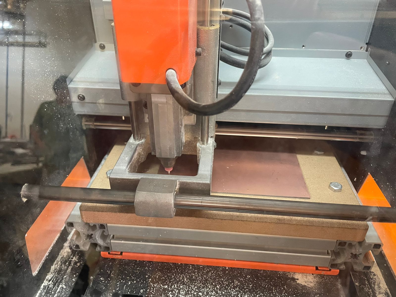
Once the files were ready, I fabricated the PCB using the MonoFab SRM-20.
To calibrate the Z axis, I used a sheet of paper similarly to leveling a 3D printer.
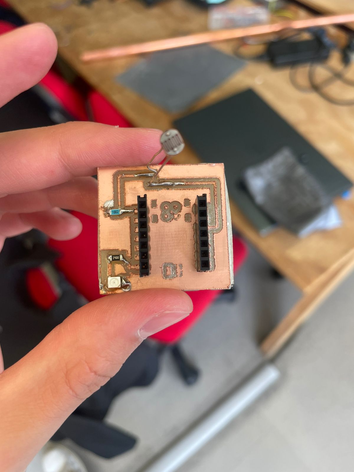
After cutting the board, I soldered all the SMD components.
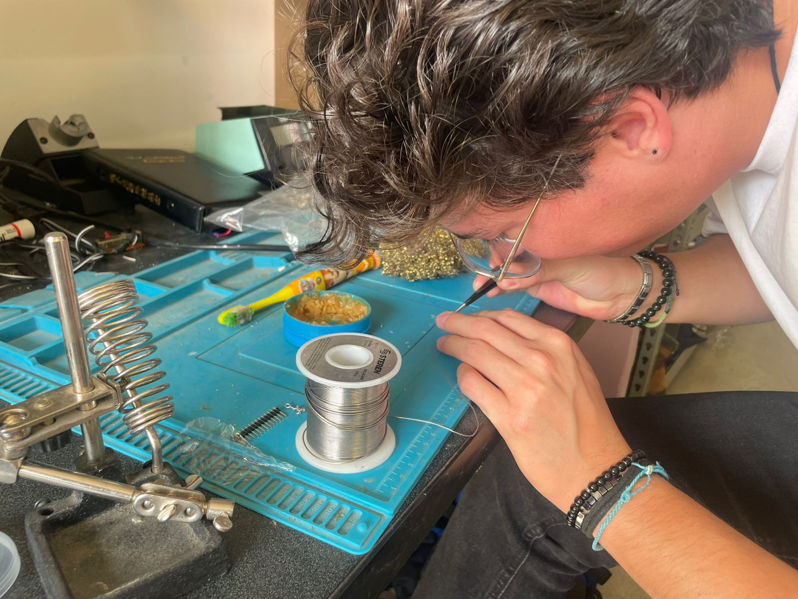
First, I applied solder to one pad. Then I fixed one side of the component and finally soldered the other side.
Since the focus of this week was PCB fabrication rather than programming, I used ChatGPT to generate a simple code where the LED changes brightness depending on ambient light.
#include <avr/io.h>

const int ldrPin = D0;
const int ledPin = D6;

int minLuz = 178;
int maxLuz = 182;

float brilloSuave = 0;

void setup() {

  Serial.begin(115200);

  pinMode(ledPin, OUTPUT);

}

void loop() {

  int ldrValue = analogRead(ldrPin);

  float normalizado =
  (float)(ldrValue - minLuz) /
  (maxLuz - minLuz);

  normalizado =
  constrain(normalizado, 0.0, 1.0);

  float brillo =
  50 + (1.0 - normalizado) * 205;

  brilloSuave =
  brilloSuave * 0.9 + brillo * 0.1;

  analogWrite(ledPin, (int)brilloSuave);

  delay(20);

}
The PCB holes were not properly milled because the cutting speed was too high.
Some traces were too thin, so I increased the trace width in KiCad.