Main Tool
KiCad for schematic and PCB design.
Fab Academy 2026
Designing my first custom ESP32 development board using KiCad and learning how professional PCB workflows work.
KiCad for schematic and PCB design.
ESP32-C3 based wearable development board.
Build the foundation of my final wearable project.
During this week’s group assignment, we worked with a multimeter, an oscilloscope and a logic analyzer to analyze electronic signals and debug circuits.
I was already familiar with using the multimeter and oscilloscope for measuring voltage, continuity and signal behavior over time, but the logic analyzer was completely new to me.
I found the logic analyzer especially useful for debugging microcontrollers because it allows you to visualize digital communication signals and verify if the microcontroller is actually transmitting data correctly.
After using it during this assignment, I realized how valuable it can be for embedded development, especially when troubleshooting communication or programming issues.
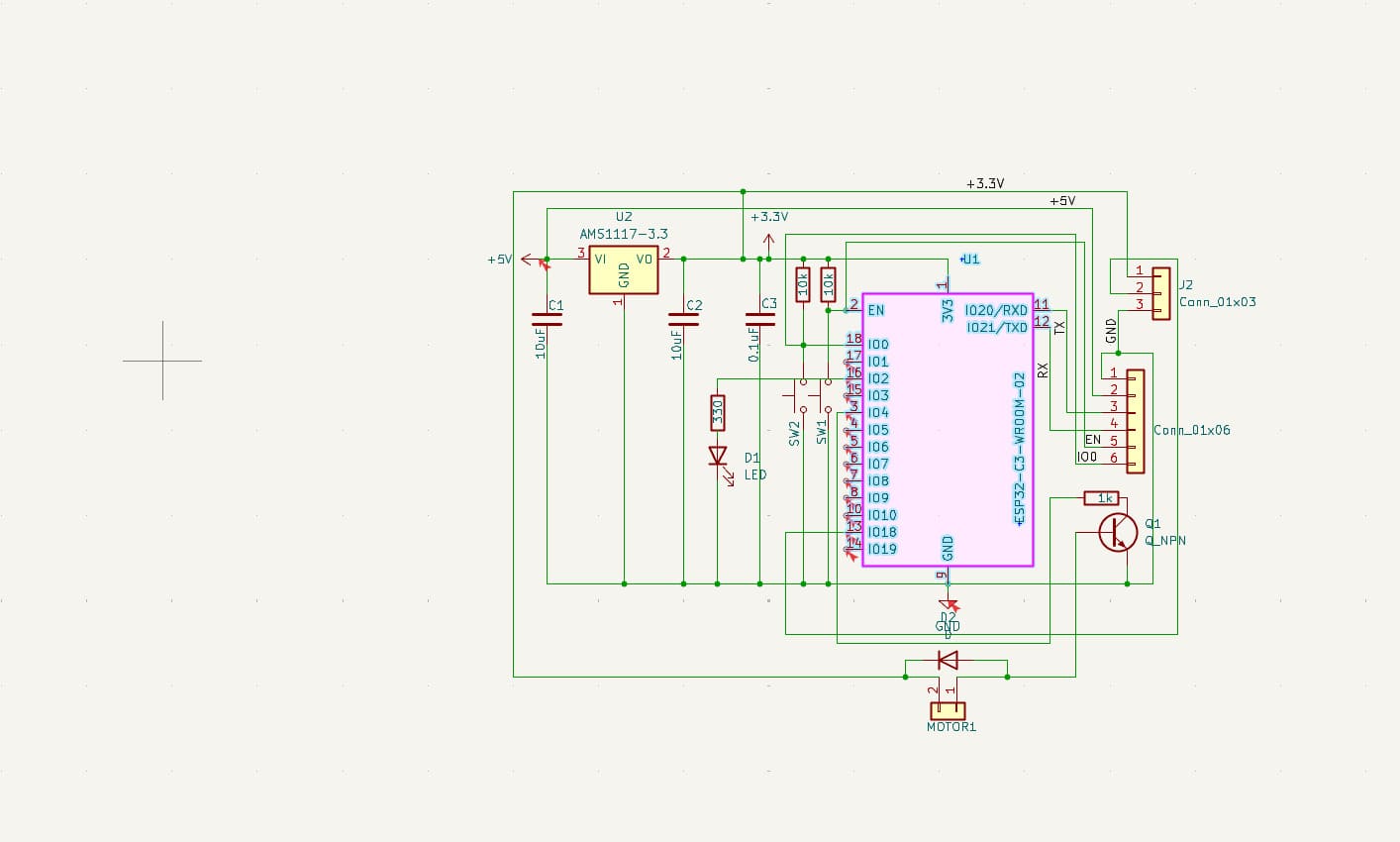
Group Assignment – Electronics DesignFor this assignment, I used KiCad to design a custom development board based on the ESP32-C3 microcontroller.
The board includes power regulation, programming headers, user inputs, LED feedback and a motor driver for vibration control.
KiCad Official WebsiteMain microcontroller with integrated WiFi and Bluetooth.
Voltage regulator that converts 5V into 3.3V.
Used for voltage stabilization and noise filtering.
User interaction inputs connected with pull-up/pull-down resistors.
Controls the vibration motor safely from the ESP32 GPIO.
Visual feedback system for breathing guidance and status indication.
The schematic was developed step by step, starting from the ESP32-C3-WROOM-02 and progressively adding the required support circuitry.
I selected the ESP32-C3 because of its integrated WiFi, low power consumption and enough GPIO pins for my wearable application.
The board is powered using a 5V input that is regulated down to 3.3V using the AMS1117 voltage regulator.
Two 10µF capacitors were added at the input and output of the regulator to stabilize the voltage.
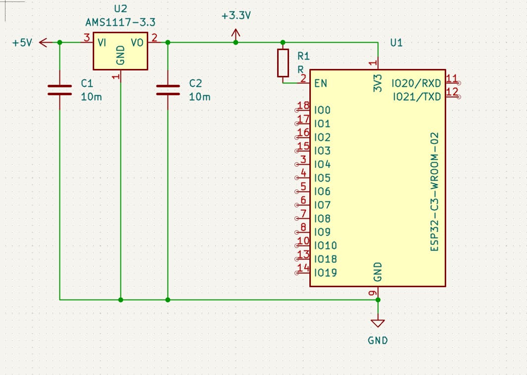
Two push buttons were included for user interaction. Each one uses a 10kΩ resistor to avoid floating signals and ensure stable logic levels.
A 1x06 programming header was added for serial communication and programming access.
A 0.1µF decoupling capacitor was placed close to the ESP32 to reduce high-frequency noise and improve stability.
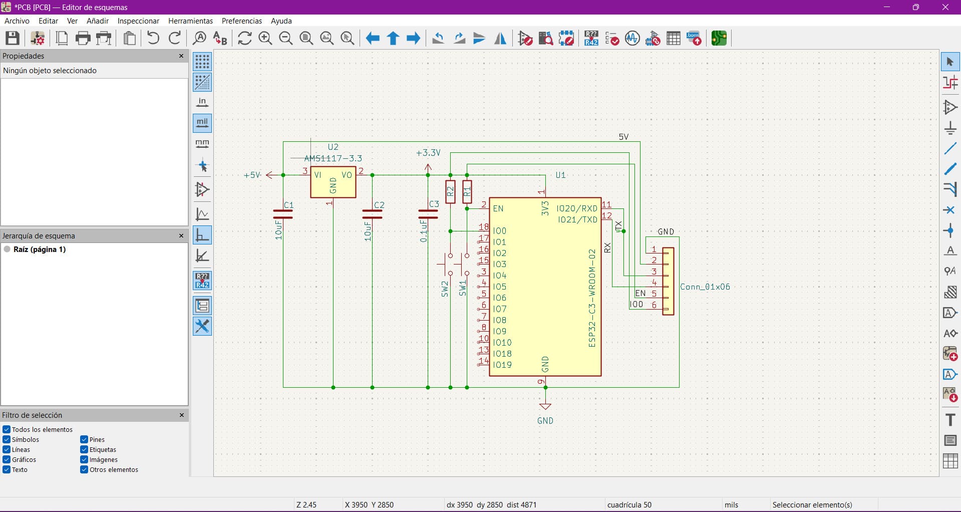
Since the vibration motor requires more current than a GPIO can safely provide, I used an NPN transistor as a switching device.
A flyback diode was added in parallel with the motor to protect the transistor from voltage spikes generated when the motor is turned off.
Finally, I added an LED for visual feedback and extra headers for motor connection and expansion.
Here is the final schematic:
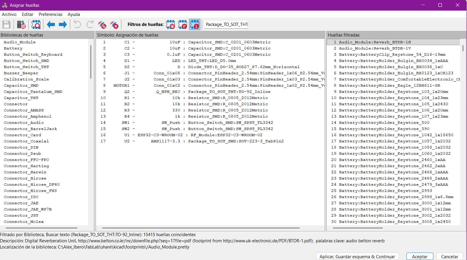
After completing the schematic, the next step was assigning footprints to each component.
This process is essential because schematic symbols only represent logical connections, while footprints define the real physical pads and dimensions used in the PCB.
During this stage, I carefully verified that the pin numbering of each symbol matched the pad numbering of the assigned footprint.
Since KiCad connects components based on pin numbers instead of names, incorrect assignments can easily create routing errors.
Once the footprints were assigned, I transferred the schematic to the PCB editor to begin the layout process.
Initially, all components appeared grouped together with only airwires showing the electrical connections between them.
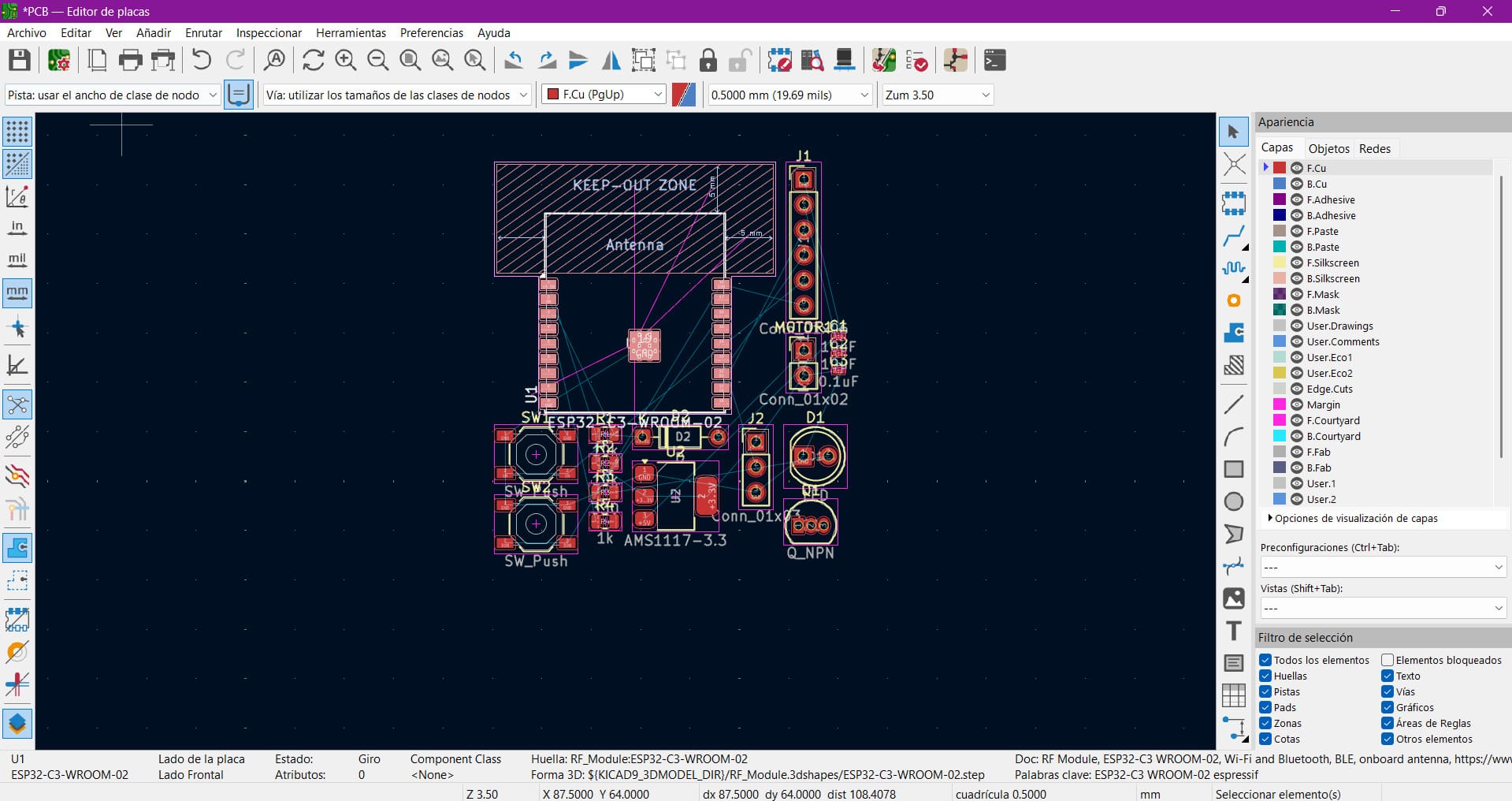
During the first placement attempt, I tried organizing the components to reduce airwire crossings and improve routing flow.
However, I noticed that some components were placed too close to the antenna area of the ESP32 module.
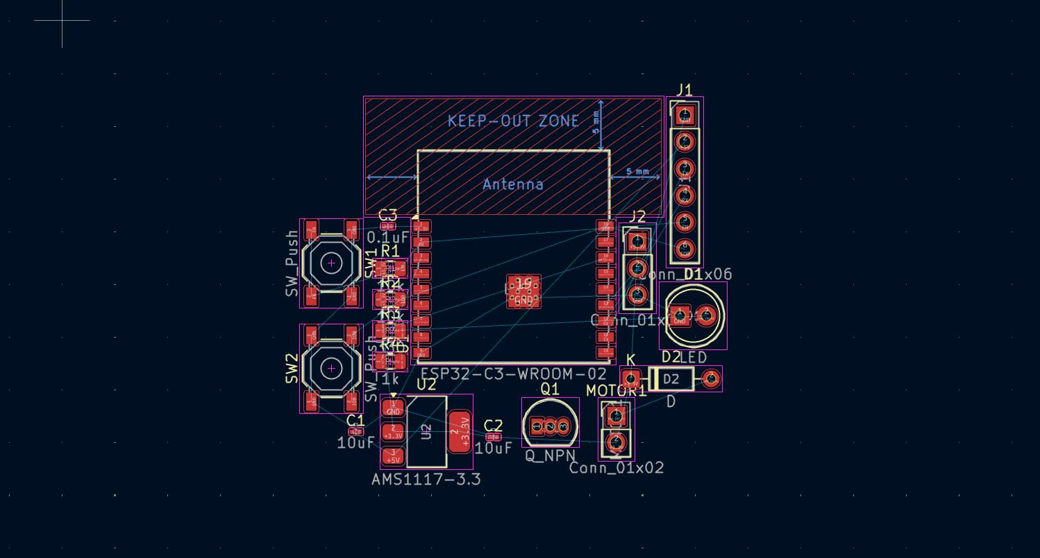
Since the ESP32 uses an integrated PCB antenna, it is very important to maintain a keep-out area around it.
No traces, copper planes or components should be placed near the antenna because they can negatively affect WiFi performance.
After identifying this issue, I reorganized the layout and moved the components away from the antenna zone.
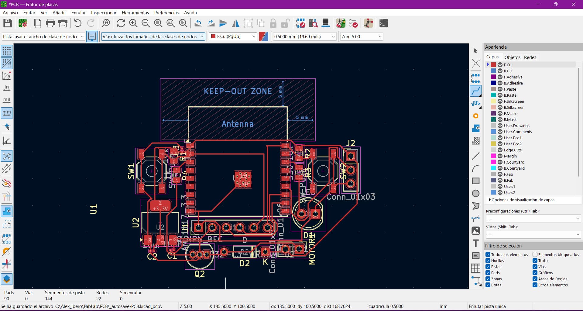
After completing the schematic and PCB layout, I ran the Design Rule Check (DRC) to verify the board before manufacturing.
The DRC checks electrical connectivity, spacing violations, trace widths and unconnected nets to ensure the board meets manufacturing requirements.
This step is extremely important because even if the PCB visually looks correct, small clearance or routing issues can cause the board to fail after fabrication.
This PCB design is directly connected to my final project because it is intended to become the main control board for my wearable device.
The board integrates the microcontroller, power regulation, programming interface and output control into a single compact system.
However, this is still not the final iteration.
Throughout the Fab Lab process, I will continue refining the design based on testing results and performance improvements.
I still need to verify if the board dimensions are small enough for a bracelet form factor.
The layout may be redesigned to improve compactness and comfort.
This board will eventually connect the sensor, motor and feedback systems of Ancora.