

6. Electronics Design
This week of Fab Academy is all about designing and milling your own PCB with a microcontroller and successfully making it do something. In this case I will be using the MicroPython code from Week 4 to turn on LEDs using a Seeed Xiao RP2040.
Week 6 Group AssignmentSimulating Circuits
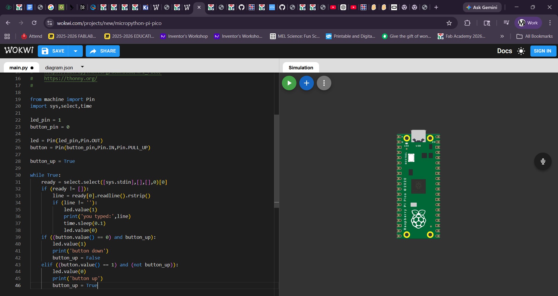
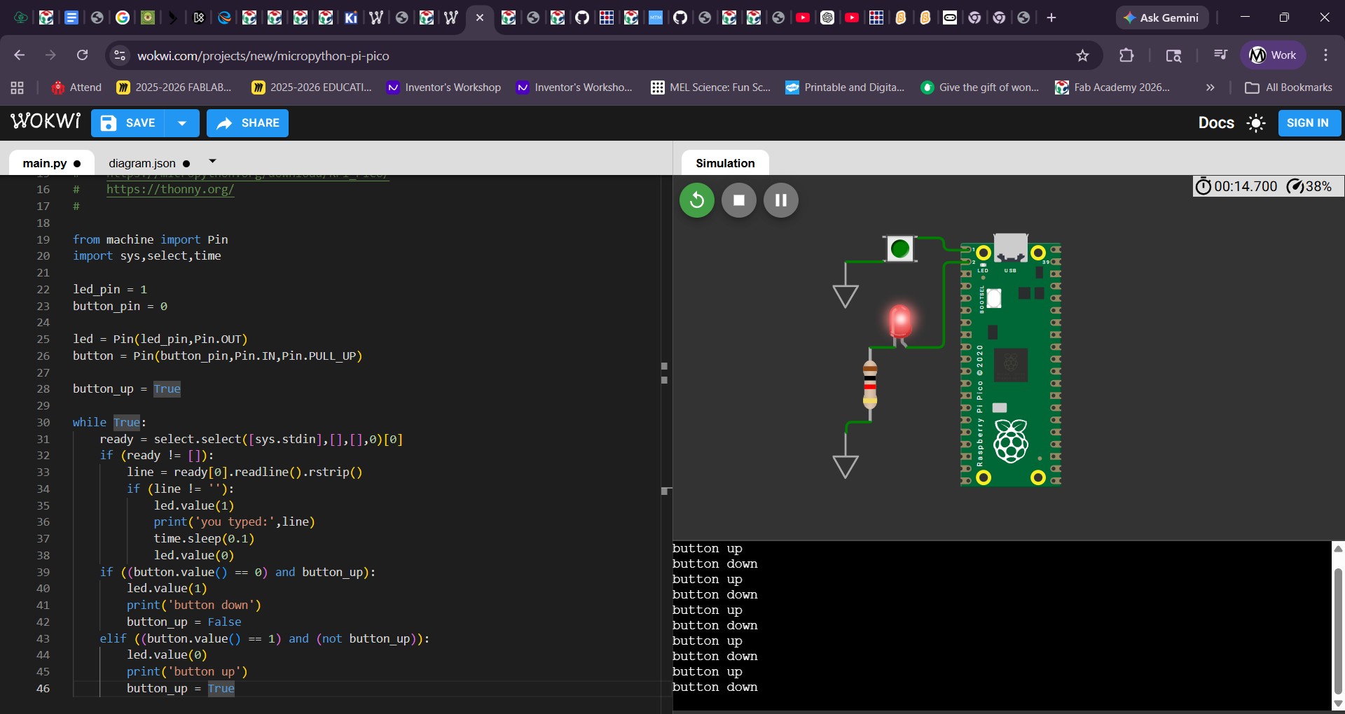
This week of Fab Academy is all about designing and milling your own PCB with a microcontroller and successfully making it do something. In this case I will be using the MicroPython code from Week 4 to turn on LEDs using a Seeed Xiao RP2040.
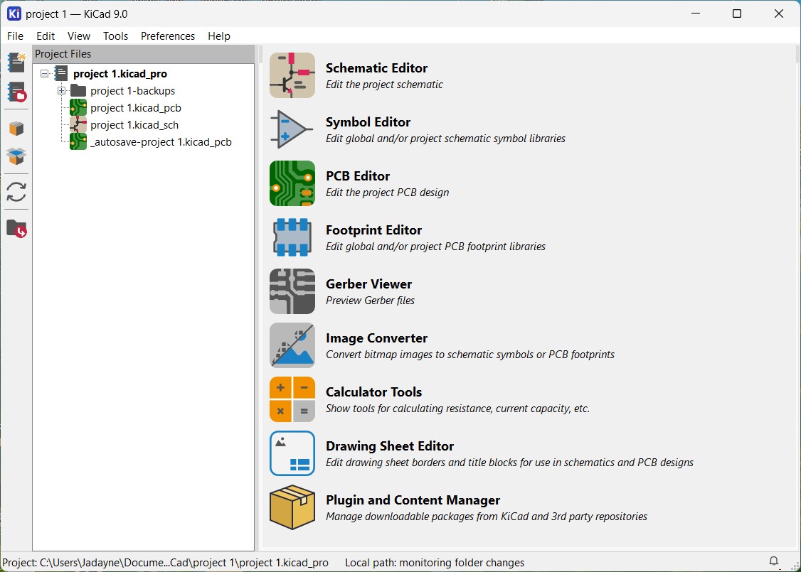
Next I needed to learn about PCB design. This led me to KiCad. I started a first test project with the schematic and PCB files.
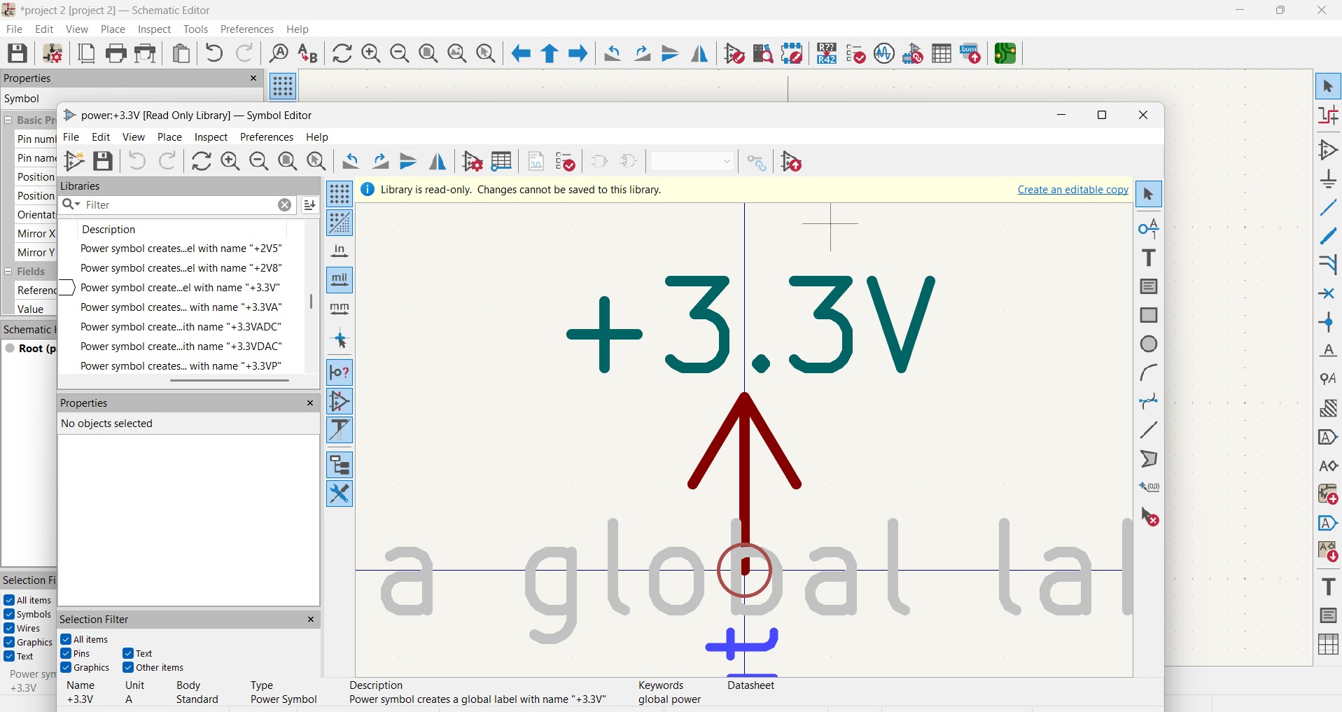
It took a while to get used to the interface of the schematic editor so this attempt was more about understanding how to add components and make connections.
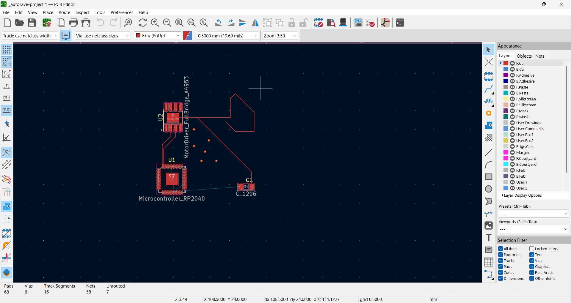
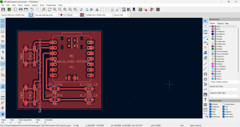
The experiment continued in the PCB editor. It would take a few more steps in my learning process to understand how to utilize these tools.
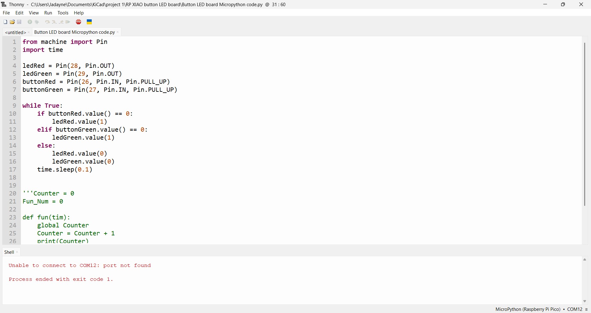
Looking over the MicroPython code in Thonny with Alie, a member at Moonlighter FabLab, I was able to understand more about connecting the RP2040 microcontroller to Thonny and manipulating the code.
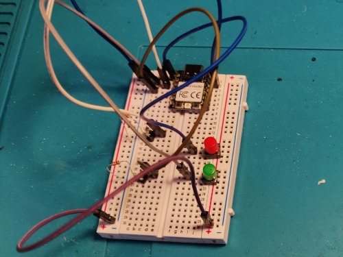
She was also a huge help when we assembled the components on a breadboard. This was my first time seeing a physical circuit layout on a board presented in a clear and logical way. I really appreciated her assistance.
 Link to YouTube Video

This Youtube tutorial taught me how to use the tools and symbols in KiCad.
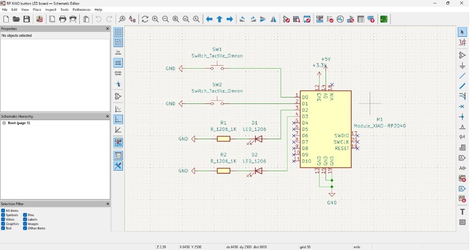
I returned to KiCad to create a proper schematic of the PBC. I still wasn’t fully confident but I followed the logic of how electric currents flow. My logic may have been a little off because I still think I put the resistors in the wrong place.
Group Project
Testing the PCB data signals with a Logic Analyzer has revealed a clear rise and fall when the switch is pressed and the LED blinks.
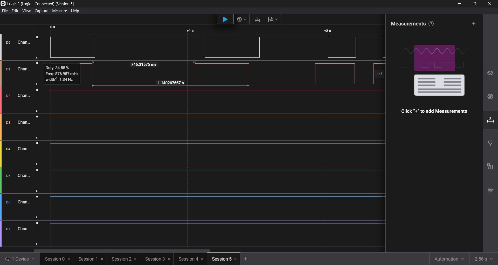
The switch was connected to Channel 1 and the Led was connected to Channel 2. You can see that Channel 1's base line is consistently low when idle, while Channel 2's is high. These values are inverted when the switch is pressed. This happens almost simultaneously and with similar wave lengths. My conclusion is that the each component has a value on a binary; a 1 and a 0. when an input is detected, the value flips which causes the value of the connected component to also flip.
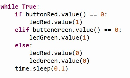
While writing this conclusion, I remebered that the Micropython script actually mentions this logic. The Logic Analyzer has confirmed the logic in the code.