WEEK 06
Electronics Design
How the week started
Stepping back into unfamiliar territory once again, I’m hoping that the documentation from Week 4 will guide me through this week’s work. This week feels more technical from a beginner’s perspective, but for someone with an electronics background, it would probably be just the tip of the iceberg in the vast world of electronics.


How the week ended
By the end of this week, I found myself constantly questioning the basics where does this connection go? Does this component need to be grounded? Does it require a voltage supply? I was trying to recall the fundamental concepts I had previously learned. Although designing in KiCad became much easier after completing one model, I still felt lost throughout the overall process. At many points, I felt like I was working without fully understanding what I was doing.
Week 06’s Assignment
Group assignment:
- Use the test equipment in your lab to observe the operation of a microcontroller circuit board (at minimum, demonstrate the use of a logic analyzer).
- Document your work on the group work page and reflect on your individual page what you learned.
Individual assignment:
- Use an EDA tool to design a development board that uses parts from the inventory to interact and communicate with an embedded microcontroller.
Group Assignment
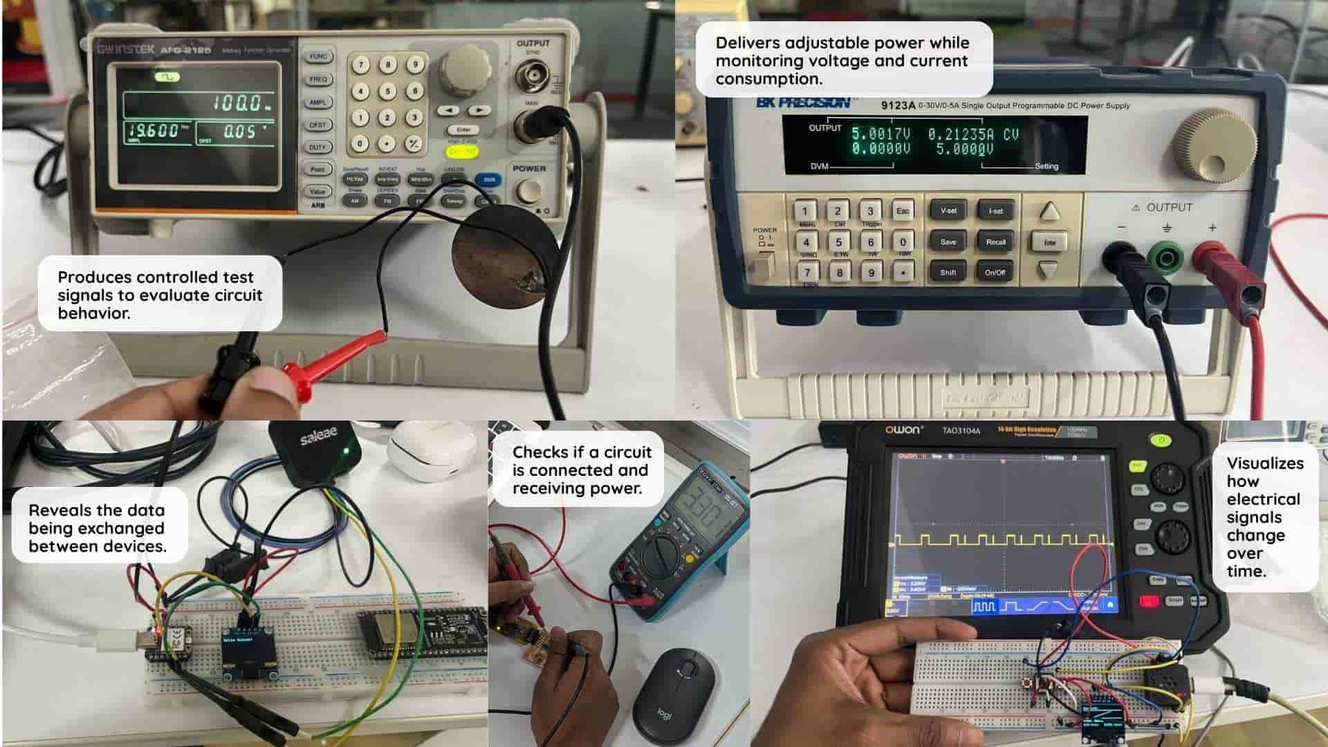
These pieces of equipment help us to troubleshoot the connections.
Bench Power Supply: If we have a board to test rather than relying on our power adaptors, this equipment provides a highly stable, adjustable source of voltage and current.
Digital Multimeter: If I have powered the board using the bench power supply, I also need to know if the connections are working fine. This equipment measures voltage (V), current (I), and resistance (R), and checks for continuity.
Oscilloscope: A multimeter is good for steady voltages. To understand how the voltage changes with time, this equipment graphs voltage on the Y-axis against time on the X-axis, allowing us to actually "see" the electricity. It shows if electrical noise or interference is messing up your signals.
Logic Analyzer: It captures multiple digital signals simultaneously and decodes them into readable formats.
Function Generator: The device produces controlled test signals to evaluate circuit behavior. If I don't have a sensor, this machine can mimic the signal of that sensor and I can test the board.
Notes ▼
Key Technical Terms
- Pin Type: The electrical property assigned to a component pin (Input, Output, Power Input, Passive).
- Net: A group of pins and wires that are electrically connected.
- Cross-probing: The ability to click an error in a list and have the software automatically locate and highlight that issue in the schematic.
▲ Close Notes
KiCad
Why Design Digitally?
KiCad is an open-source Electronic Design Automation (EDA) software used for designing electronic schematics and printed circuit boards (PCBs). It provides a complete workflow from circuit design to PCB layout and manufacturing file generation.
That is the technical explanation. In simple words, it is a place where we can design the PCB digitally instead of using a breadboard. But why do it digitally?
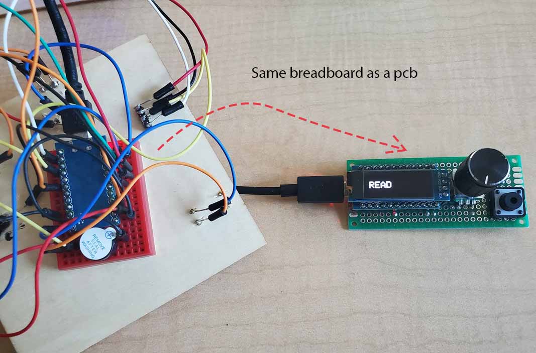
For larger designs, it is a much better approach. By designing it digitally, I can mill the board and create a much neater, professional-looking component. Imagine having to carry a breadboard everywhere without losing the connecting wires or forgetting which wire goes where. With a digital design, we can solder the parts onto a milled board so they stay put.
Designing digitally also allows me to:
- Test the connections before miling
- Arrange the components based on our needs
- Create boards for desired shape
- Test the 3d model of the pcb board
- Ensure a better fit inside a 3D model or enclosure.
Since it is open source and widely used in the electronics community, KiCad is a powerful tool for learning and developing professional PCB designs.
KiCad Software Setup – Installation
Offcial websiteRefernce for Downloading and installing KiCad
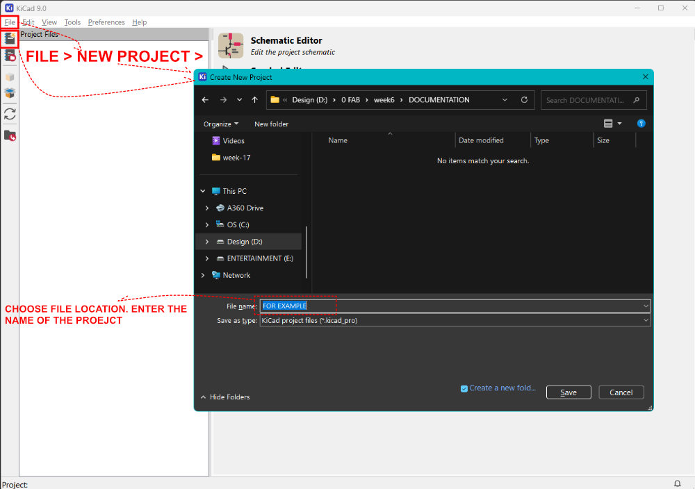
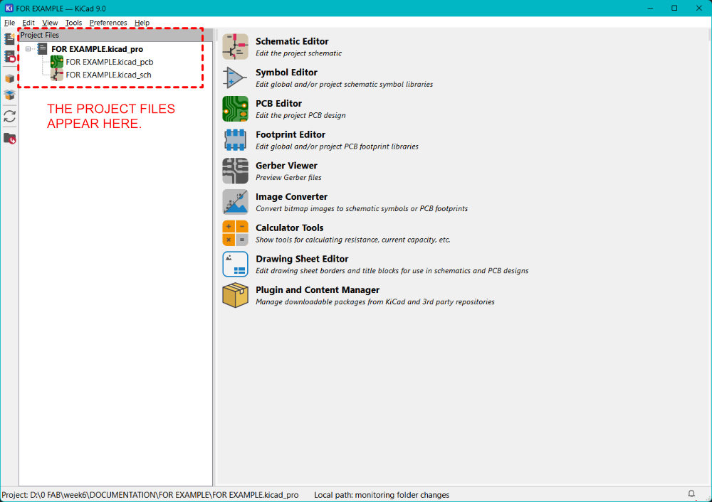
Create New Project in KiCad

Electronics Design – Recreating My Button-Controlled LED in KiCad
During Week 4 – Embedded Programming, I built a Button-Controlled LED Blinking circuit using the Seeed XIAO RP2040 on a breadboard.
This week, instead of depending on photos and videos of the breadboard setup, I recreated the same circuit using KiCad. Honestly, this felt much more practical. Once the model is saved as a file, I can revisit, edit, and reuse it without rebuilding everything physically.
We were first guided step-by-step by our instructor Saheen to create one model together. After understanding the workflow, this is where I designed my own version independently.
Understanding KiCad – The Basic Workflow
KiCad has multiple working layouts (editors). For this assignment, I mainly worked in:
- Schematic Editor
- PCB Editor
- 3D Viewer
Each layout serves a different purpose, and understanding this flow made the process much clearer.
.jpg)
To start, I created a new project by going to File → New Project in KiCad. I selected a location, gave the project a name, and saved it. This automatically created the project folder along with the schematic and PCB files linked to it.
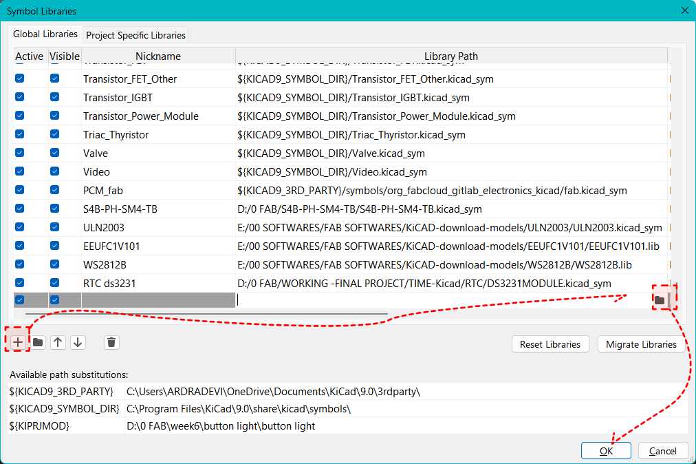
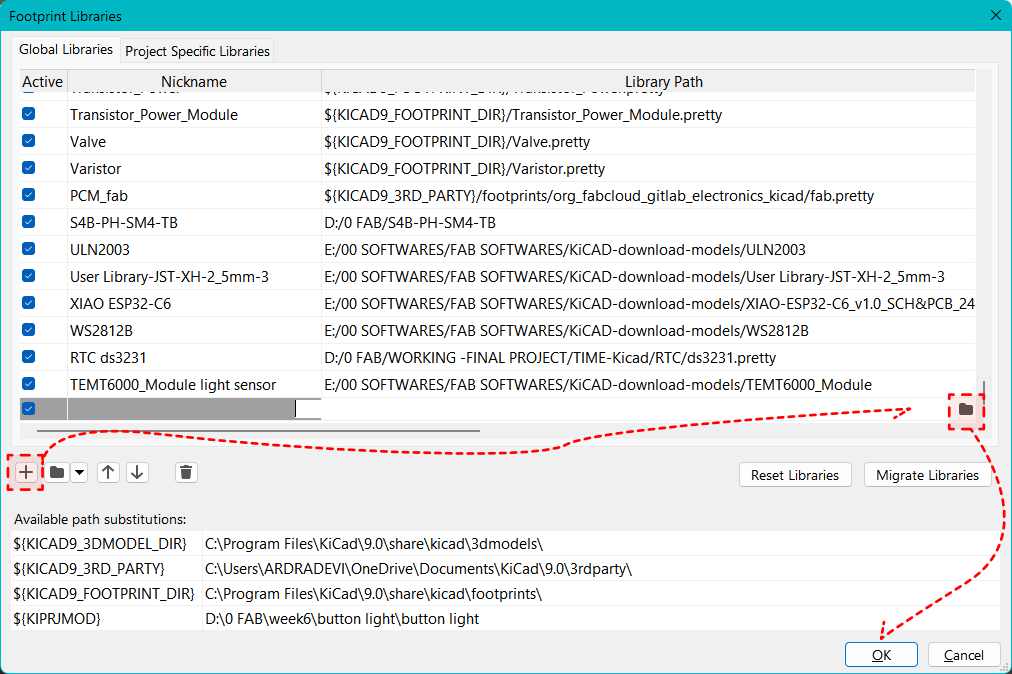
Installing the Fab Library
Before adding components, I installed the Fab library so that we all use standardized components. Fab Library
- Open KiCad
- Go to Plugin and Content Manager
- Go to the Libraries tab
- Search for KiCad offical repository
- Install KiCad FabLib
- Click Apply Pending Changes This step is essential to download the library.
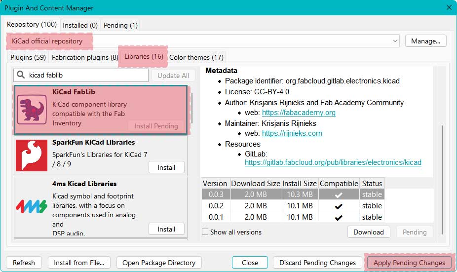
This ensures everyone uses the same symbols and footprints.
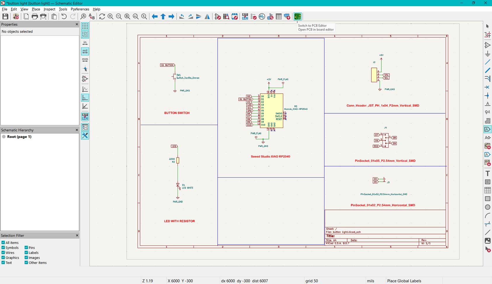
Schematic Editor – Logical Circuit Design
After creating the project, I clicked on the Schematic Editor. When it opened, it looked similar to an architectural drawing template a blank working sheet where I could start placing elements and organizing the layout. This is where I create the logical version of my circuit. It is not about physical placement, but about defining the electrical connections between components.
.jpg)
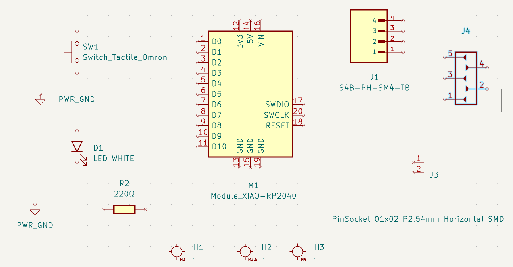
Custom Xiao PCB
Components placed
Shortcut: Press A to open the Add Symbol dialog box.
From the Fab library, I searched and placed:
- XIAO RP2040
- LED (1206)
- Switch
- Resistor
- Ground (GND)
- +5V
- Horizontal SMD
- Vertical SMD
- JST 4 PIN
KiCad - Adding symbols
I have added the exact names of the footprints I have used, so I can refer to them if I am recreating it. The footprint can be downloaded and added, and it can also be edited.
.jpg)
.jpg)
.jpg)
.jpg)
.jpg)
.jpg)
.jpg)
.png)
.jpg)
Importing from snapEDA
Some componets may not be availanle on fab library, thsoe we can download from external libray. we use snapEDA/SnapMagic THE SITE
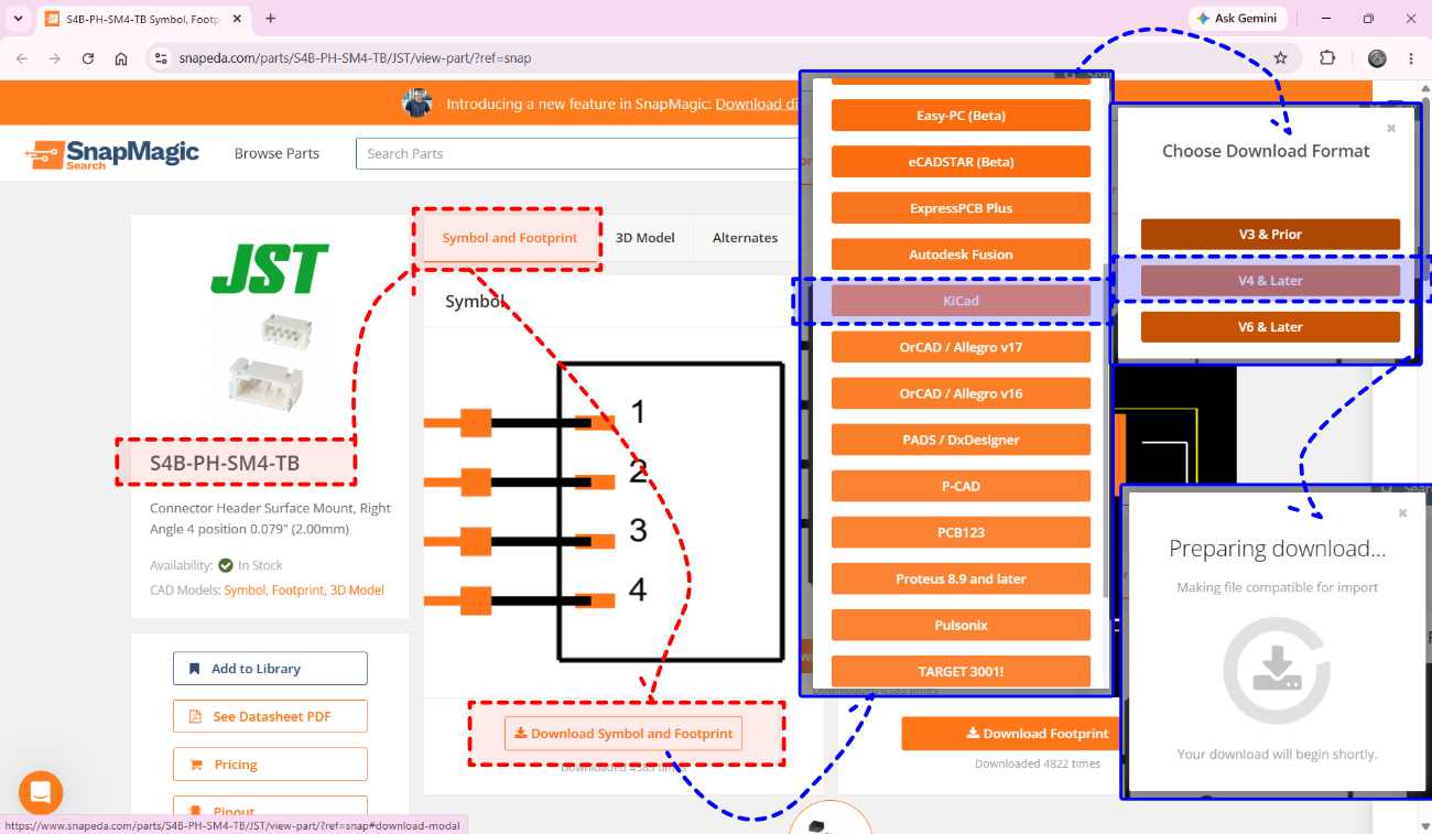
S4B-PH-SM4-TB - Connector Header Surface Mount, Right Angle 4 position 0.079" (2.00mm)
Download -LinkRenaming A Symbol or component
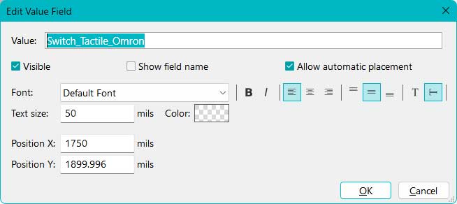
I can double-click on the component's name to edit it. The names can be customized for self understanding, or deleted if not required.
Rotate
The components can be rotated by pressing "R". There is also an option to flip the module. However, when flipping the component, it might become upside down, so that needs to be kept in mind while doing so.
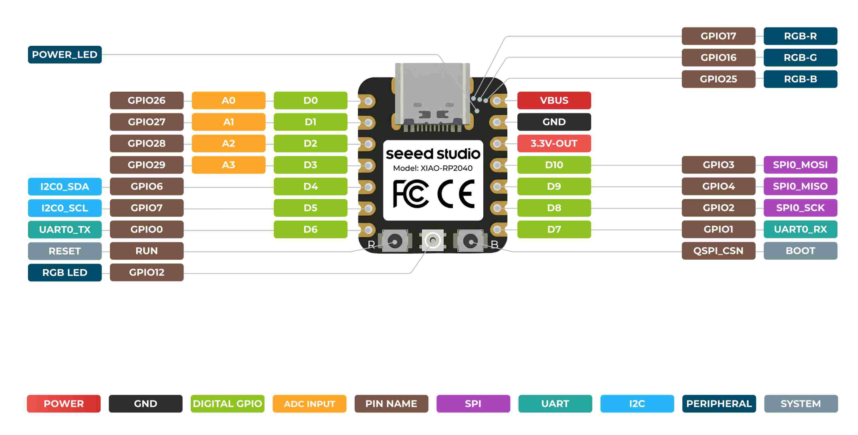
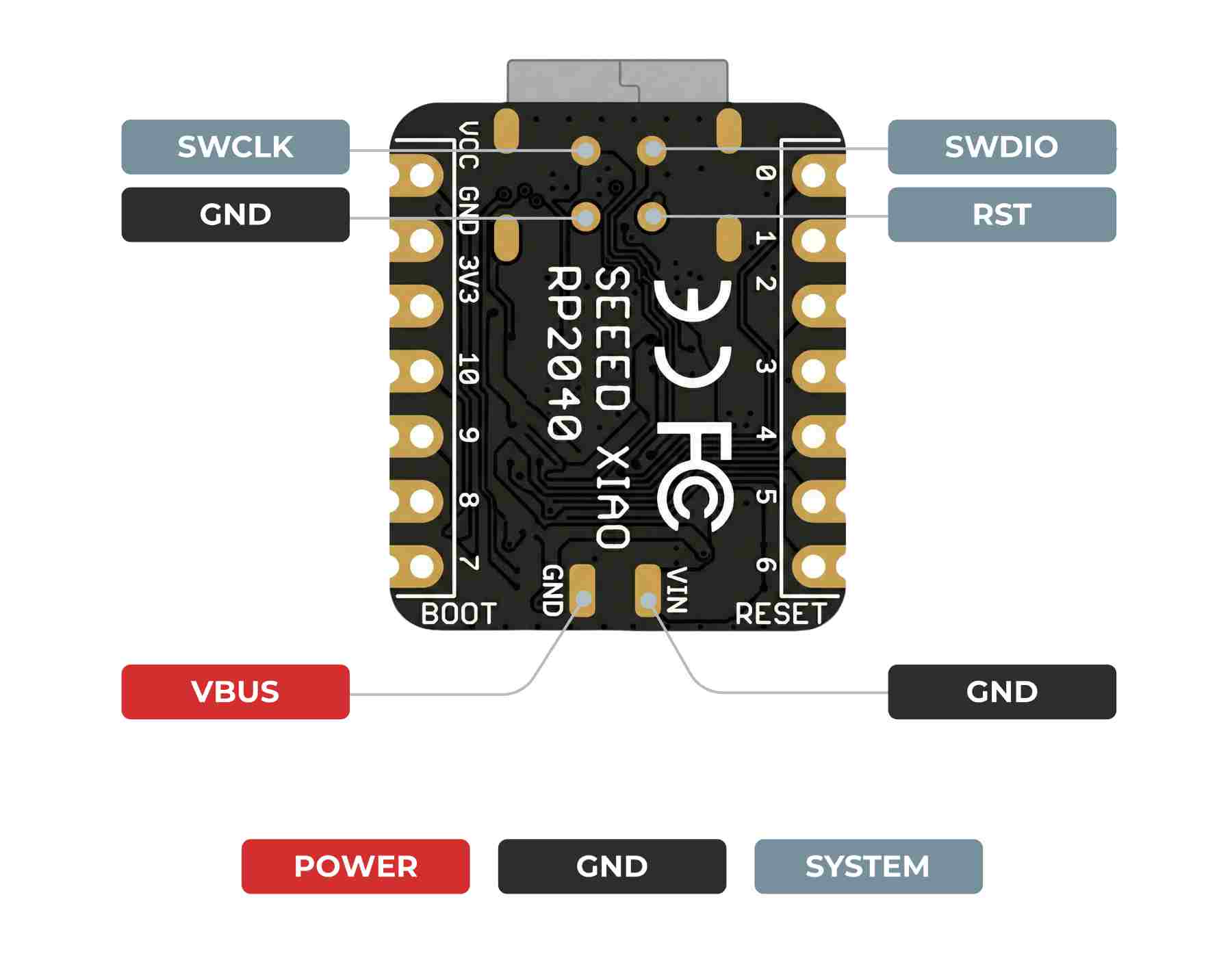
Seeed studio xiao-rp2040 pinout diagram
Components Placed
The components are placed on the schematic editor. The connections are to be drawn.
Connecting Components – Two Methods
Method 1: Drawing Wires
Shortcut: Press W. I can draw wires directly between component pins. This creates visible electrical connections, but can become messy in complex circuits.
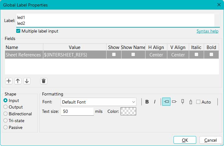
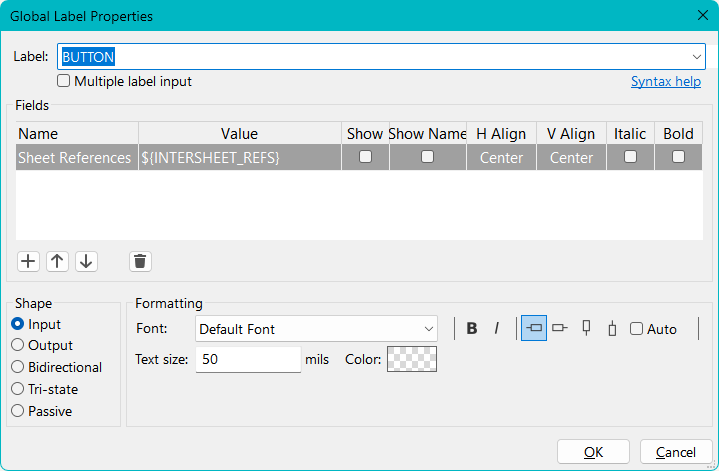
Method 2: Using Net Labels (Cleaner Method)
Instead of drawing long wires, I used net labels.
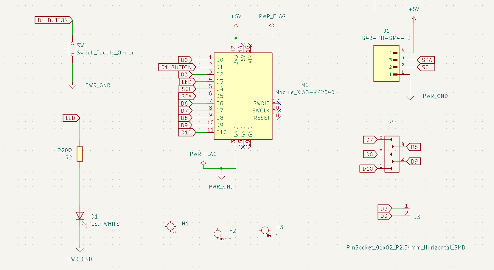
- Select the Place Global Labels tool from the right toolbar
- Place it at the end of a component pin
- Give it a name
For example:
- I labeled the LED connection as LED
- I labeled pin D3 on the XIAO as LED
If two nets share the same name, KiCad treats them as connected even if there is no visible wire between them.
This keeps the schematic clean and professional.
Adding Multiple Labels
If I need to add many labels:
- Select the Label tool
- Enable Multiple Placement
- Type the first label → Press Enter
- Type the next label
- Click OK when done
Understanding the Circuit Logic
Recreating the circuit digitally forced me to think clearly about:
- Where power is supplied
- Where ground is connected
- Why the LED needs a current-limiting resistor
- How the GPIO pin controls HIGH and LOW signals
- How the button interacts with the microcontroller
LED Resistor Calculation

Reference : LED Resistor Calculator - Circuit Digest and DigiKey
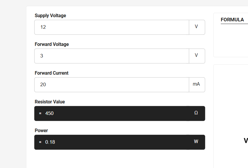
The resistor value got was 450ohms. We used the nearrest value resisotr we had - 1K ohm or 1000ohms resistor. DigiKey
The supply voltage was taken as 5V from the XIAO RP2040 datasheet. To find the LED forward voltage, a multimeter can be used in diode test mode. The probes are connected across the LED, with the positive probe on the anode and the negative probe on the cathode. The reading displayed by the multimeter gives the forward voltage of the LED. The forward current value was obtained from the LED datasheet and used for the resistor calculation.
LED Resistor - Value renaming
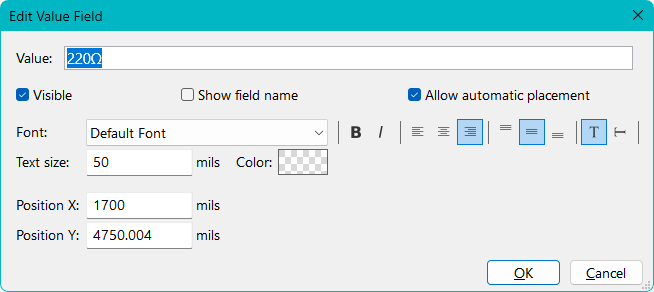
Double click on the R_1206 value written on the resistor. Change this to the resistor value obtained from the calculation, which is 1kΩ.
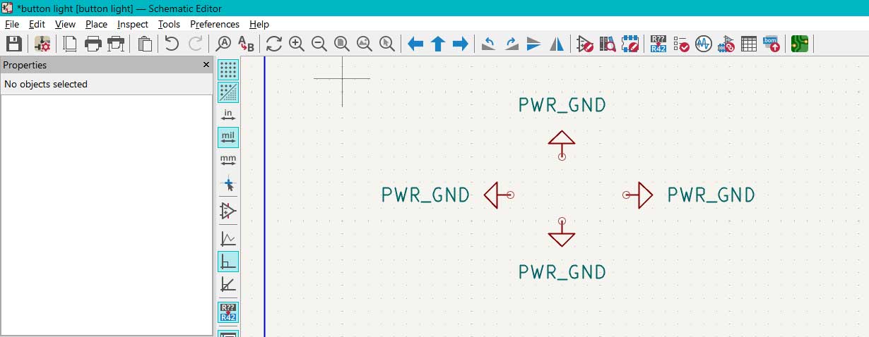
Global Label
Click on the "PLACE GLOBAL LABELS" icon in the right corner. This is used to label the conenctionsor pins.
.png)
.png)
.png)
.png)
.png)
.png)
.png)
Earlier, I depended on remembering breadboard placement. Now, I understand the logic behind each connection.
Till this stage in KiCad, I have added all the required components for my design and completed the schematic connections. I assigned the necessary symbols, connected power (VCC) and GND properly, and ensured that all input and output pins are logically mapped.
By the end of this process, I get a clear idea of how many GPIO pins are being used, how many are still available, and whether the selected microcontroller board is sufficient for the design. This step also helps me identify missing pull-up/pull-down resistors, incorrect connections, or any floating pins before moving to footprint assignment and PCB layout.
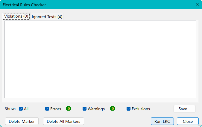
ERC - Electric rule check
Before moving to PCB layout in KiCad, I performed an Electrical Rules Check (ERC) to ensure that my schematic follows proper electrical logic. ERC helps me verify that power nets are correctly driven, inputs are not left floating, and pin connections follow valid electrical constraints.
1. Running the ERC
To begin the verification process, I selected the Electrical Rules Checker icon from the top horizontal toolbar.
.jpg)
- I opened the ERC dialog box.
- I clicked Run ERC.
- Any detected issues appeared under the Violations tab.
.jpg)
When I clicked on an error message, KiCad automatically cross-probed the issue — meaning it highlighted and zoomed into the exact component or net in my schematic that caused the error.
2. Troubleshooting: "Input Power pin not driven"
One of the common errors I encountered during this process was:
Error: Input Power pin not driven by any Output Power pinsTechnical Cause
In KiCad, most power pins (such as VCC or GND) are defined as Power Input pins. According to KiCad’s electrical rules, every Power Input net must be connected to at least one Power Output pin (for example, the output of a voltage regulator).
While using the breadboard, I powered the XIAO board using a Type-C cable connected directly to my system. Since this power supply connection was external, it was not explicitly shown in my schematic. However, I realized that even though the power source is physically provided through USB, it must still be logically represented in KiCad to satisfy the Electrical Rules Check (ERC).
Since I was powering my board directly from a connector or battery, there was no explicit Power Output pin in the schematic. Because of this, KiCad flagged the net as not being properly driven.
3. Resolution: Using the PWR_FLAG
To resolve this issue, I used the PWR_FLAG symbol.
The Fix
.jpg)
- I placed a PWR_FLAG from the symbol library.
- I connected it to my power nets (such as VCC and GND).
The Result
The final ERC without errors.
By adding the PWR_FLAG, I informed the ERC that these nets are being driven by an external power source. This satisfied KiCad’s pin type requirements and cleared the error successfully.
Final Schematic diagram image
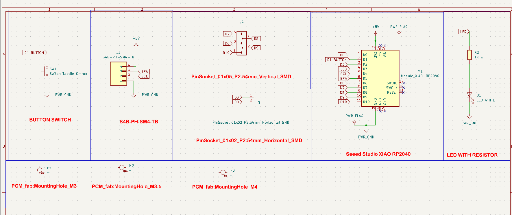
At this point, the schematic gives a complete functional overview of the circuit, making it easier to verify the design before proceeding further.
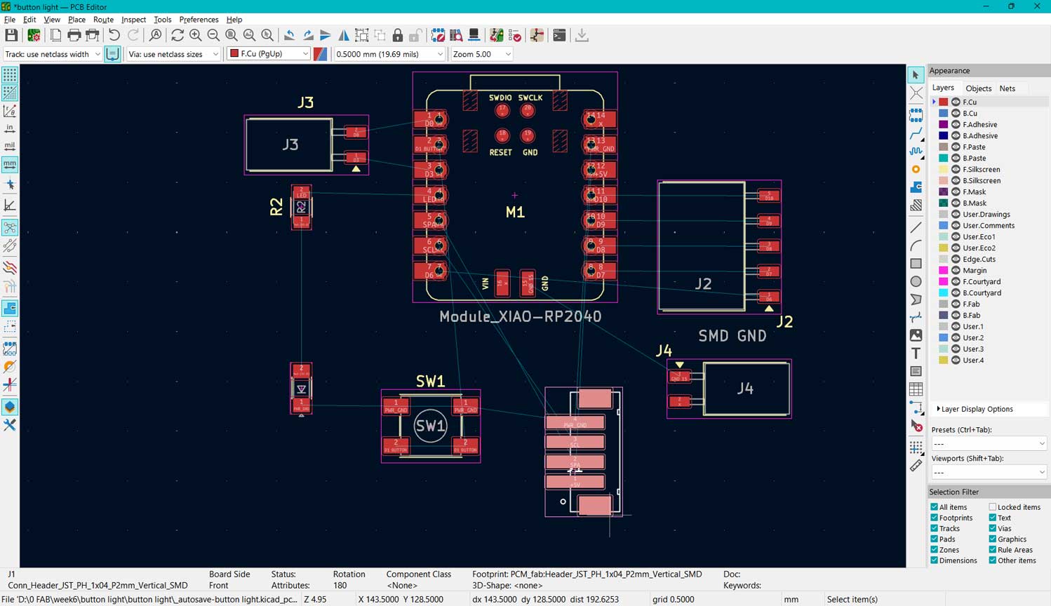
PCB Editor – Physical Board Layout
After completing the schematic and clearing all ERC errors, I moved to the PCB Editor in KiCad.This is done by clicking the last icon "Switch to PCB Editor" on the horizontal tab If the schematic is the logical blueprint of the circuit, the PCB Editor is the physical construction site. This is where the circuit transforms from connections on paper into a manufacturable board.
Unlike the schematic, PCB layout is about:
- Physical placement
- Real-world dimensions
- Routing copper traces
- Board shape and structure
- Design for fabrication
This step felt very similar to moving from concept drawings to working drawings in architecture.
Updating Components from Schematic to PCB Editor
.jpg)
I clicked the Update PCB from Schematic icon from the top horizontal toolbar (or pressed F8).
.jpg)
In the dialog box, I confirmed the update. The components were then imported into the PCB Editor in their real footprint size.
.jpg)
Understanding Footprints
In the schematic, components are symbols. In the PCB editor, they become footprints the actual physical pads and dimensions that will be soldered.
.jpg)
- XIAO RP2040 footprint defines USB position, pin spacing, and mounting orientation.
- 1206 LED and Resistor footprints define pad size, spacing, and soldering area.
Choosing the correct footprint is very important because it determines whether the component will physically fit on the board.
Arranging Components for Better Placement
Creating traces is not as simple as just drawing lines. It is a back-and-forth process rotating components, moving them slightly, rethinking paths, and sometimes even going back to the Schematic Editor to correct something. Then I return to the PCB Editor and press Update PCB from Schematic (F8) to sync the changes.
Shortcut: Press M to move components, R to rotate.
Keep in mind
Component placement is not random. It has to be placed based on the components logic and functionality:
- XIAO RP2040 placed centrally for accessibility.
- LED placed near the edge for visibility.
- Switch placed where it can be easily pressed.
- Resistor placed close to LED to minimize trace length.
- JST connector placed at board edge for external connections.
While placing components, I considered short trace paths, clear routing space, no overlapping footprints, and logical grouping of related components.
Board Setup
- Track width
- Clearance rules
- Copper layer settings
- Board thickness (default settings used)
This ensures that the PCB follows fabrication constraints.
Design Rule Setup / Board Setup
Before importing the components, I first defined the manufacturing constraints. This step is critical because the PCB must follow the fabrication limits of the milling machine or board house.
- Go to File → Board Setup
- Navigate to Design Rules → Constraints
- Set the following values:
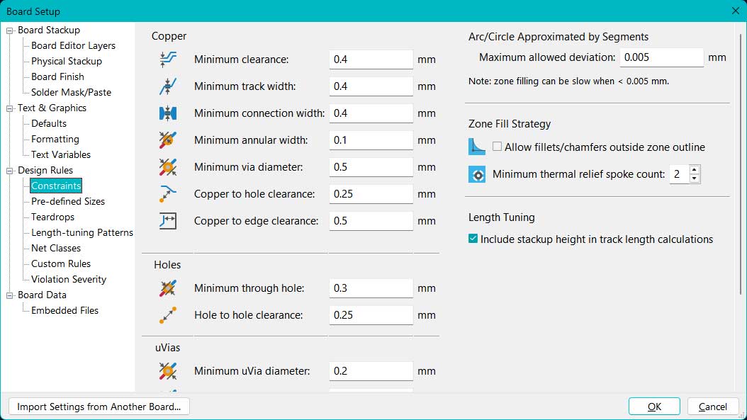
- Minimum Clearance: 0.4 mm
- Minimum Track Width: 0.4 mm
- Minimum Connection Width: 0.4 mm
These constraints define the minimum spacing between copper features and the minimum width of traces. Setting them early ensures that routing decisions automatically comply with fabrication safety limits.
Drawing a wire between pads
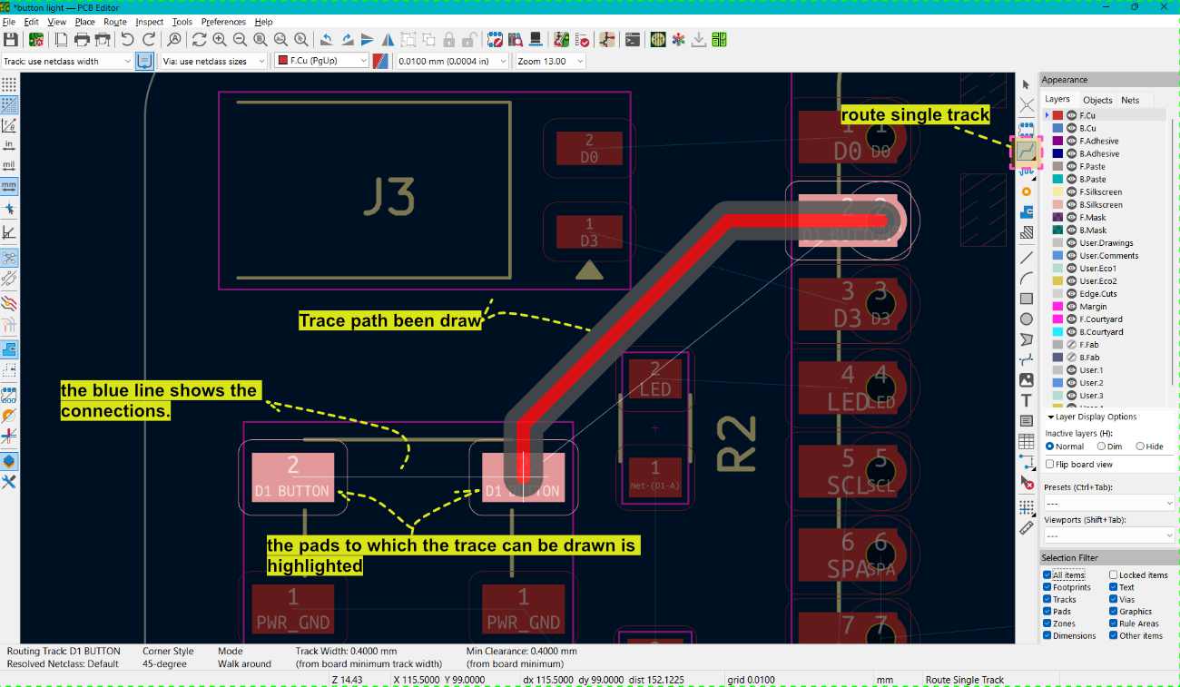
Click the icon or press X to draw the traces. When you select a pad, it automatically highlights the pads to which it can be connected. The blue lines visible are the connections drawn in the schematic. The trace thickness is 0.4 mm. The layer selected is F.Cu, which is the front copper layer of the PCB. If a double sided PCB is used, traces can be routed on both the front and back sides. In that case, B.Cu is selected for the back copper layer. The traces on the B.Cu layer appear blue, and the components on that layer are also shown in blue.
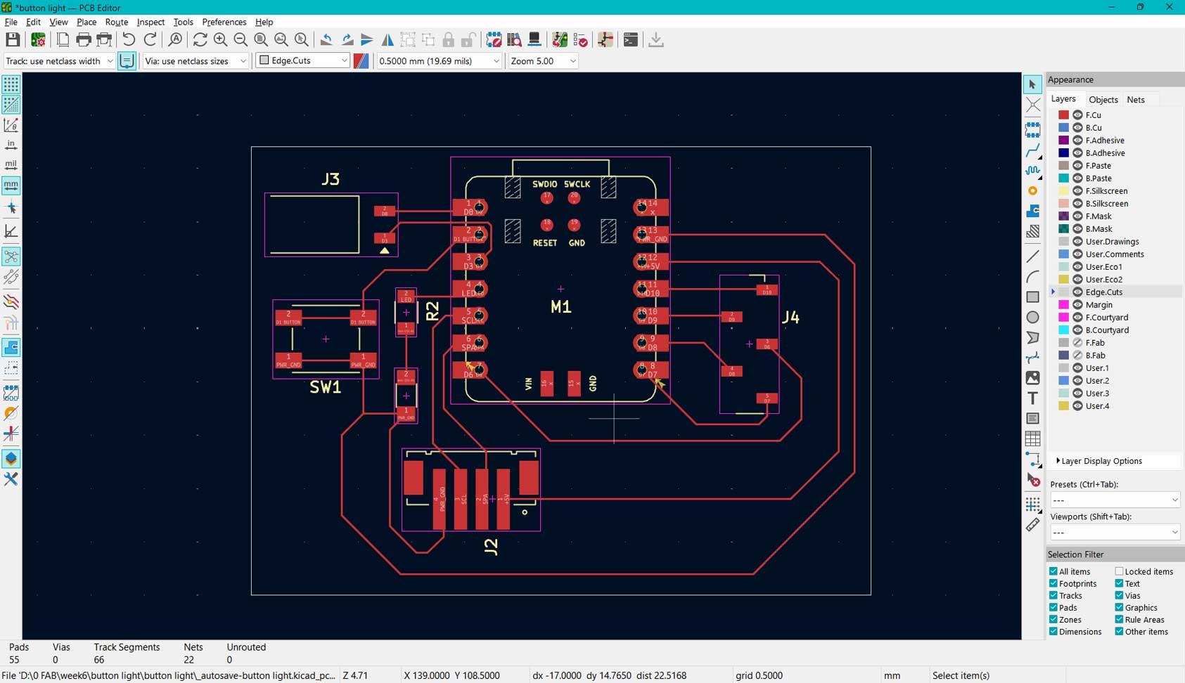
Edge cut drawing
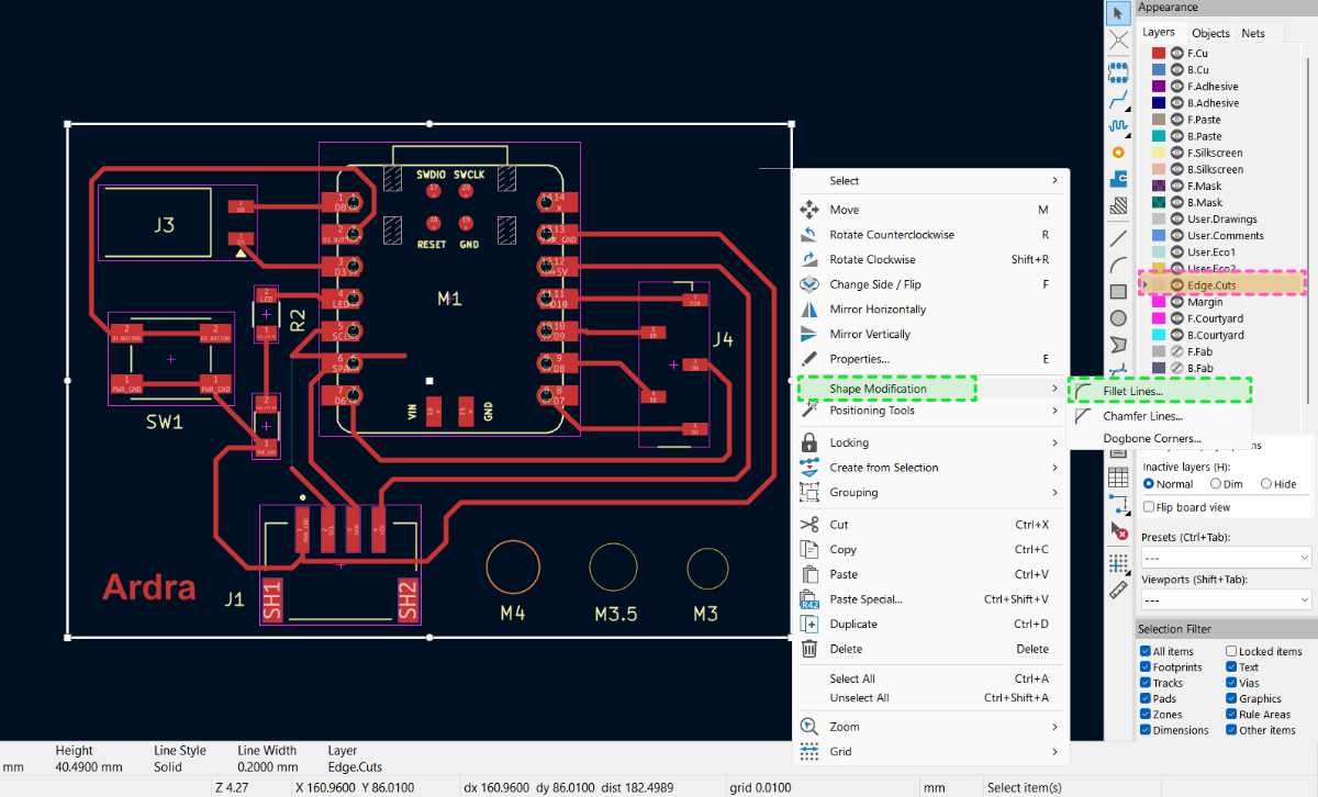
The rectangle is drawn using the Rectangle tool. The layer must be set to Edge.Cuts. To modify the rectangle, right click and select Shape Modification → Fillet Lines.
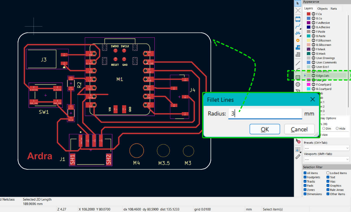
I entered a radius value of 3 mm and clicked OK. The edges became curved, removing the sharp corners. After applying the fillet, the rectangle is broken into individual line and arc segments. The Edge.Cuts layer defines the board outline, and this is the outline that will be cut by the milling bit.
Silkscreen - Adding name on top layer
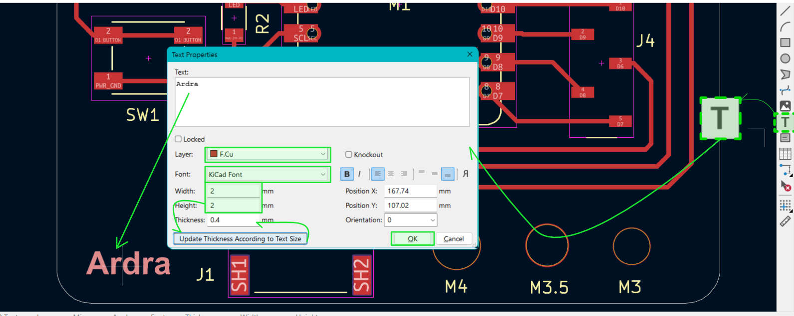
The Text tool is used to add text. Click the text icon and enter the required text in the dialog box. Check the layer name and select F.Cu, since I am using a single sided PCB. Enter the font width and height, then click "Update Thickness According to Text Height". This automatically updates the thickness value. Once satisfied with the settings, click OK. If the thickness is too small, the copper parts of the letters may become weak and can break or peel off easily during milling or soldering.
PCB Editor Layout
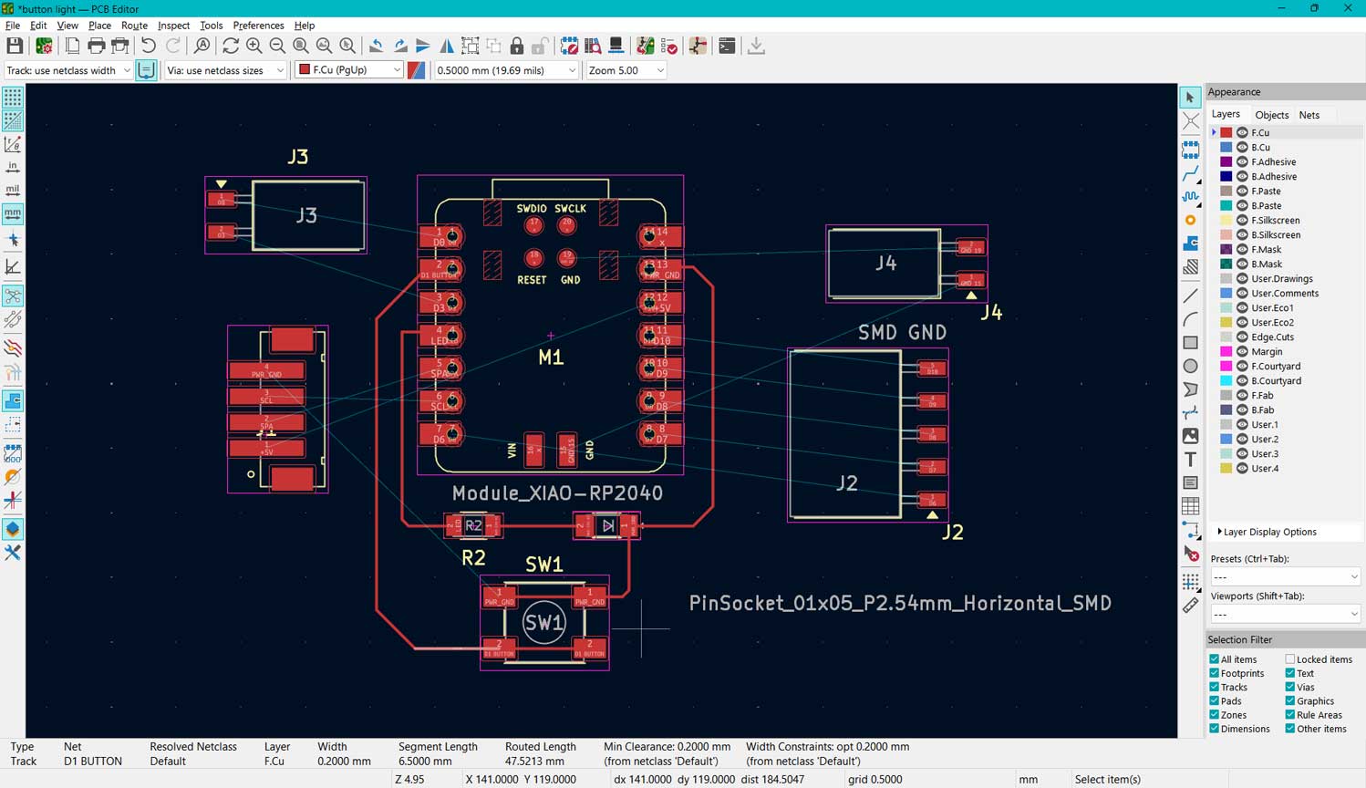
Core Actions I Do During Routing
- Press X to activate Route Single Track.
- Follow the ratsnest (blue guide lines) to connect pads.
- Keep traces short and direct wherever possible.
- Rotate components (R) and move them (M) to reduce crossings.
- Press U to select a full track path, then Delete if rerouting is needed.
- Re-run DRC if necessary to verify no rule violations.
If I try to overlap traces from different nets, KiCad immediately blocks it because of the clearance rules. If pads belong to the same net, copper continuity is allowed. This automatic rule enforcement prevents accidental short circuits.
When a connection is successfully routed, the corresponding blue ratsnest line disappears. That visual feedback helps me track which nets are completed and which still need work.
Placement Thinking (Before Final Routing)
- Position frequently connected components closer together.
- Keep power traces wider when required.
- Avoid unnecessary 90° corners.
- Leave space between traces for manufacturability.
- Place connectors and power ports along board edges.
Reflection – What I Learned
Initially, I forgot to properly consider the placement of the XIAO module. When I checked the design in the 3D Viewer, I realized the USB port alignment was not practical. That small step of viewing the board in 3D made a big difference.
I went back, adjusted the placement, updated the PCB, and re-routed the affected traces.
At this stage, routing became slightly fun almost like solving a puzzle. It is not just about connecting pins anymore. It is about thinking physically: accessibility, spacing, fabrication limits, and how the board will exist in real life.
DRC (Design Rules Checker)
This is used to check whether the traces are drawn correctly. The software cross references the traces with the labels. However, the placement and arrangement of the components must be planned and designed by us. For example, I would need the XIAO to be placed at the edge of the board so that it is easy to connect the Type C cable to transfer data. I should not place another component in front of it and block access.
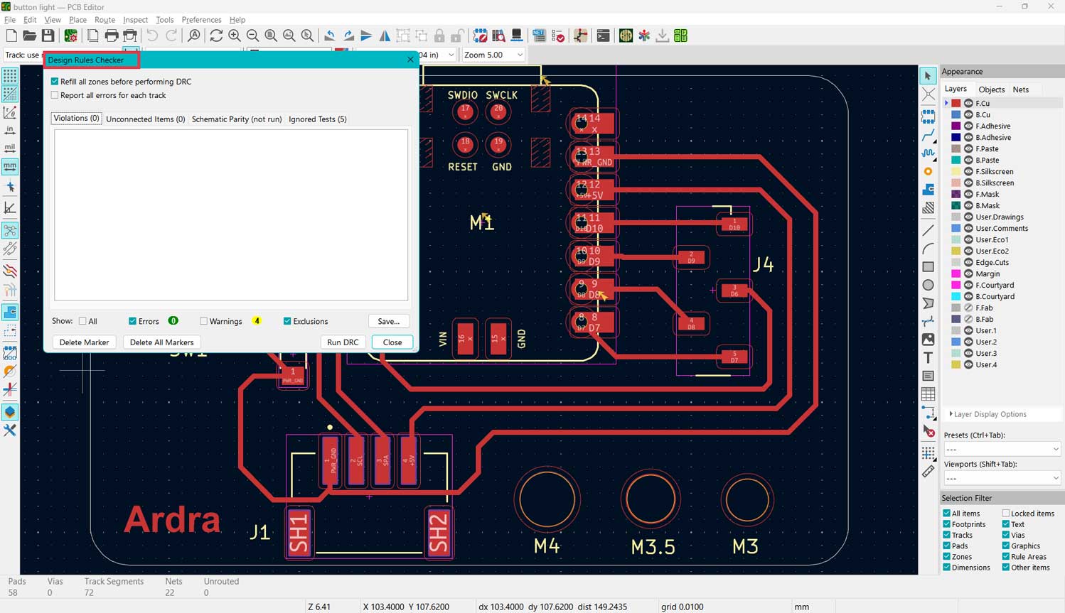
Somehow, in the first attempt, I got no errors.
Extras That Help
- Use the 3D Viewer to check component alignment.
- Zoom in closely when routing tight areas.
- Keep checking the board edges and mechanical fit.
- Update from schematic whenever changes are made.
This workflow ➜ move, route, check, adjust, update ➜ repeats until the board is clean, logical, and manufacturable.
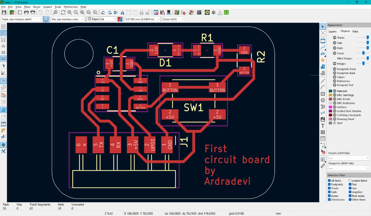
Final PCB Layout Image
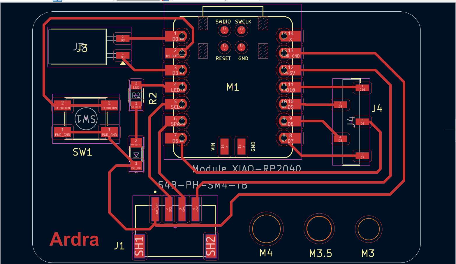
This was the final output of the layout. The traces are checked - drawn in F.Cu layer. The shape - rectangle with filleted corners drawnon Edge.Cuts
Notes ▼
Tools used
To erase a trace, I selected one segment and pressed U. This selects the entire connected track (the full routed path of that net). Then I pressed Delete to remove it completely.
While routing, I paid attention to a few important technical aspects:
- I kept traces as short and direct as possible to reduce resistance and noise.
- I avoided sharp 90° corners and instead used angled paths for smoother current flow.
- I ensured power traces were slightly wider where necessary for better current handling.
- I avoided routing too close to board edges unless required for connectors.
- I made sure clearance rules were respected to prevent short circuits.
▲ Close Notes
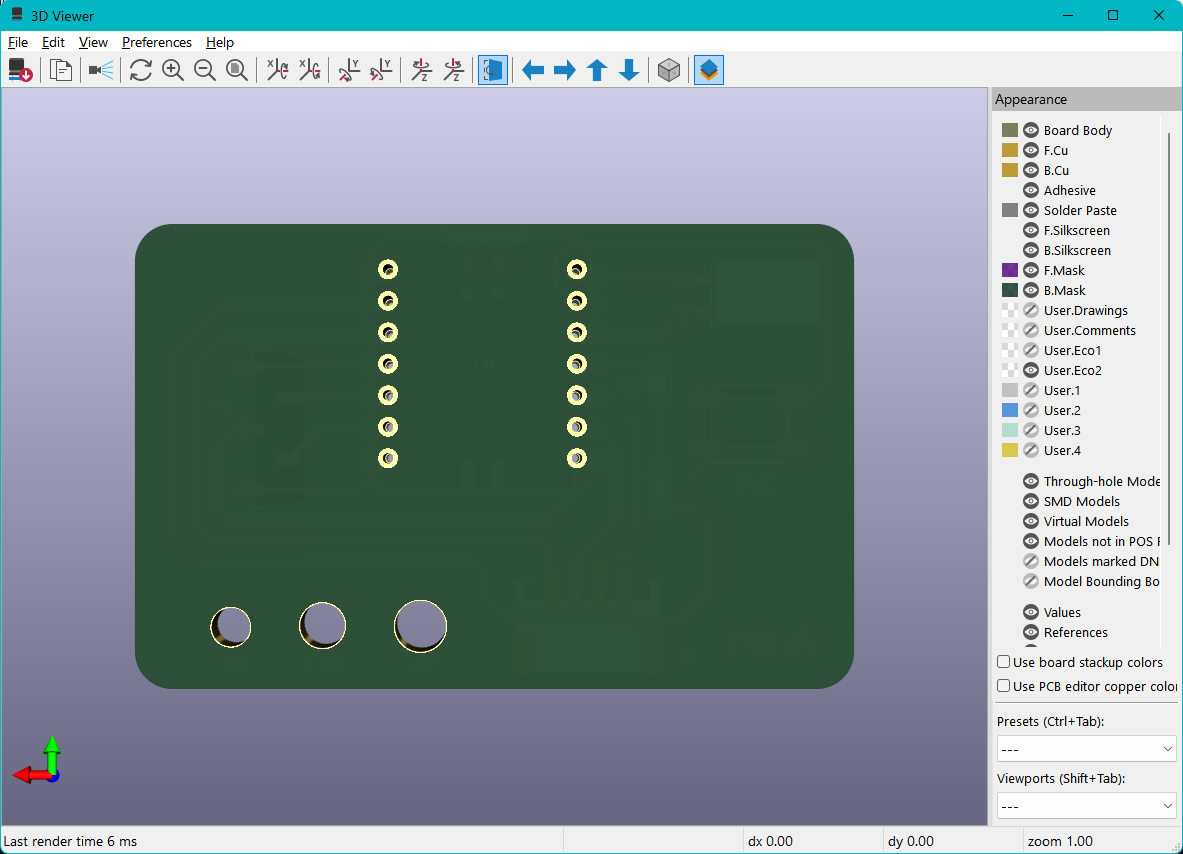
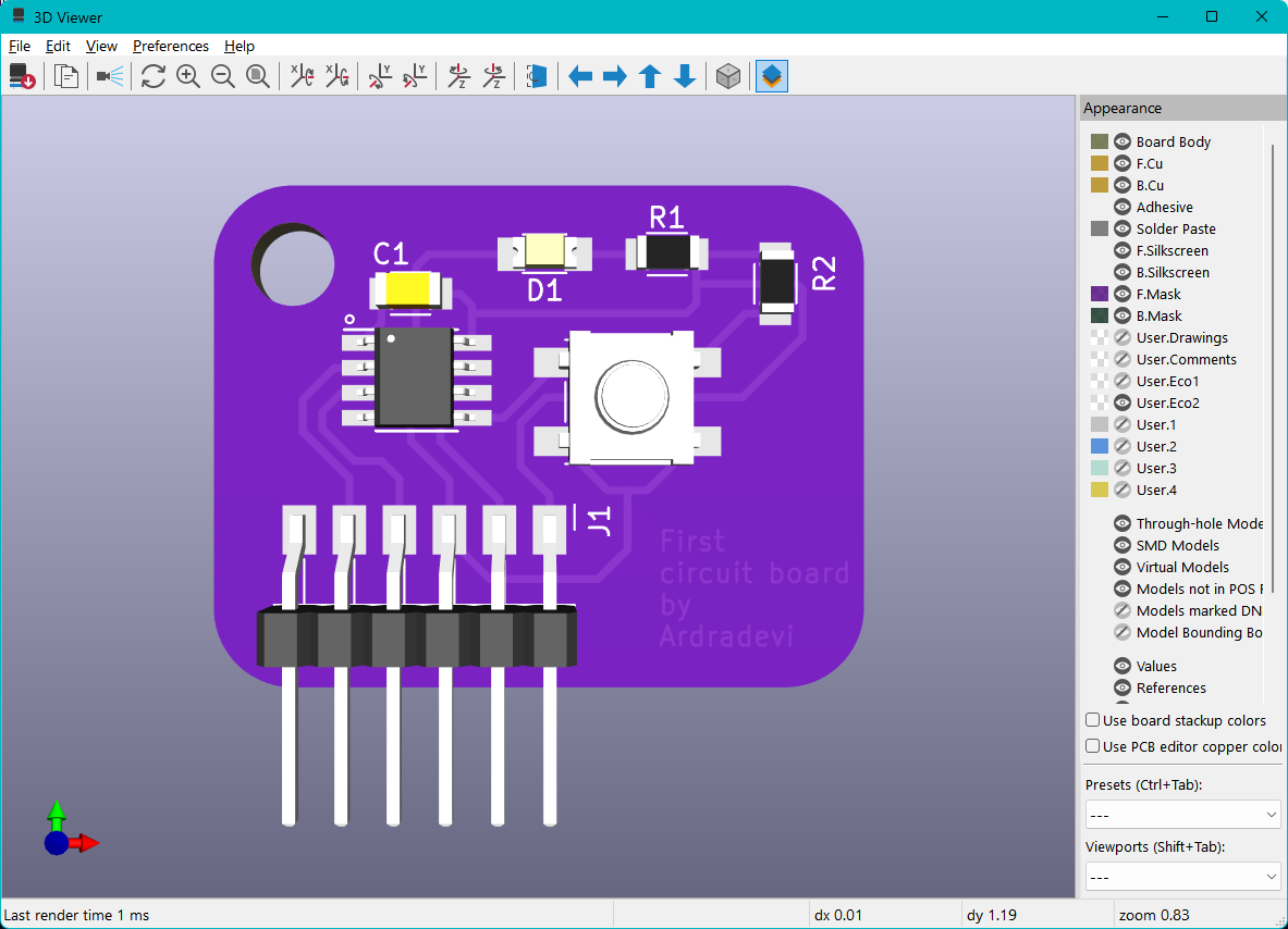
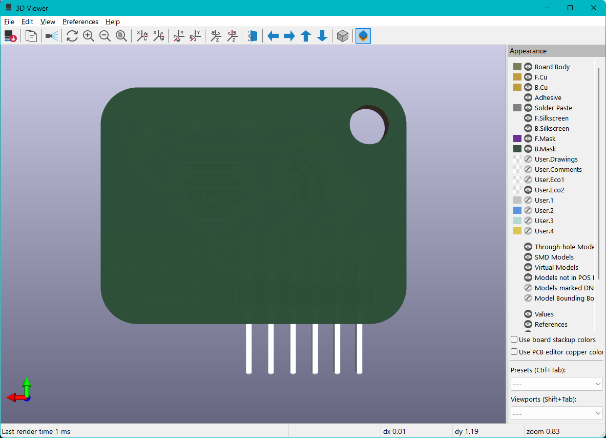
3D PCB Output
Convert the design to 3D and view
After routing, I opened the 3D Viewer.
This helped me check:
.jpg)
.jpg)
- Component orientation
- Board thickness
- Overall physical structure
- Any visible placement errors
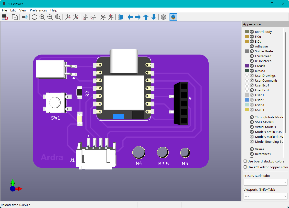
The front view of the board, the traces are milled here.
The back side of the board. the drilled holes are visible.
At this stage, the board feels real and ready for fabrication.
Gerber Files Export
Gerber files are sent to the manufacturer for fabricating the PCB. The layers are separate because they are added during different fabrication processes.
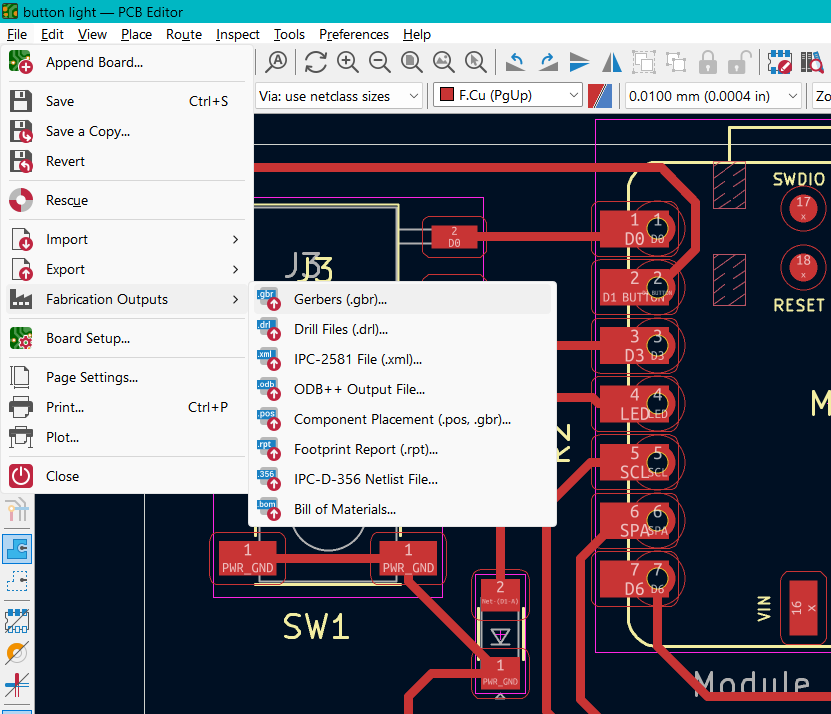
To export for fabrication: File → Fabrication Outputs → Gerber Files
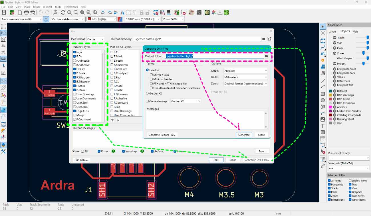
Select the layers → Click Generate Drill Files. In the Generate Drill Files window, select the output file location and click Generate. Then verify the files using PCBWay Gerber Viewer. You can see each layer separately and confirm that the traces and board outline look correct.
Gerber Files -VIEWER
we used the online Gerber viewer: pcbway and gerber2png
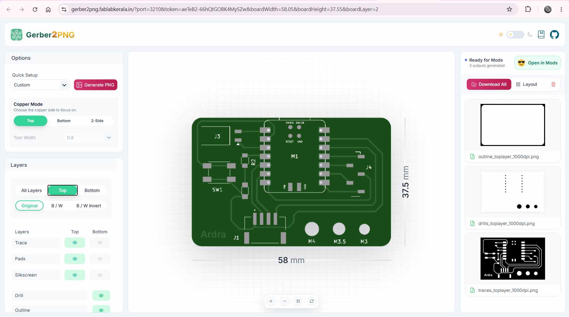
Dragged and dropped the files into the webpage and it view the gerber files.
Practice - ATtiny412
This was the first PCB . We practised on KiCad by recreating Neil's ATtiny412 blink board in Embedded Programming.
Attiny412- Pinout Diagram
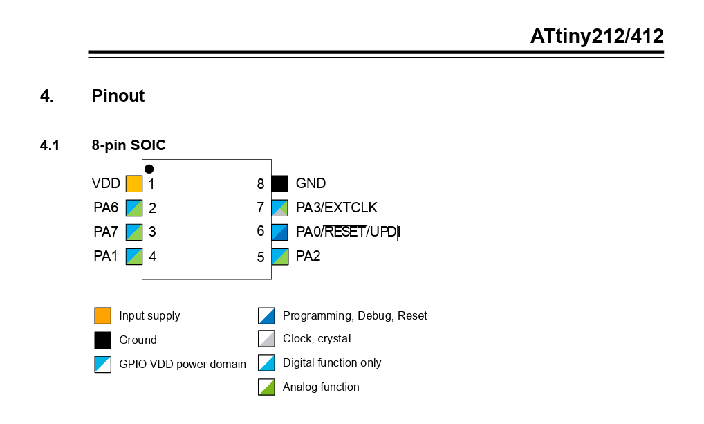
Pinout diagram of ATtiny412 DataSheet
Schematic Drawing
We tried to draw the circuit with lines and then with labels in the schematic editor.
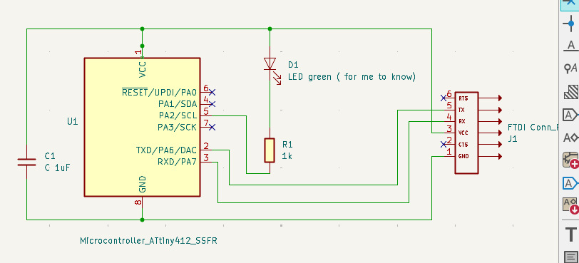
The circuit diagram connected by wires
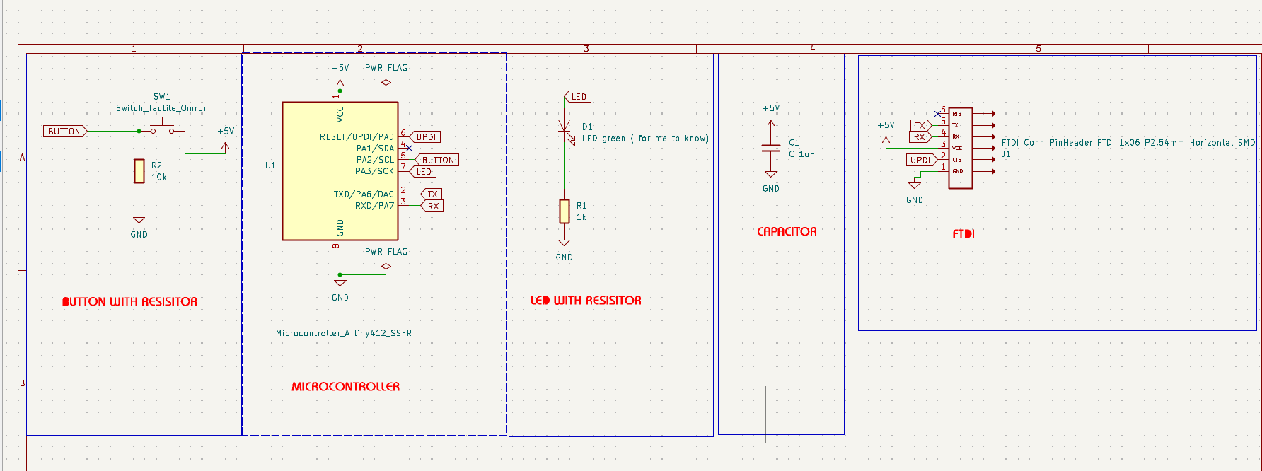
The same circuit diagram connected by labels
Place Global Label tool is used to label the connections.
PCB Layout
Traces were drawn such that traces do not have 90 degree turns. The rectangle is drawn in the Edge Cuts layer so it cuts the board off at the end.
3D PCB Output
The front view of the PCB. This shows the visual idea of the component size, placement, and orientation.
This side is flat since it has no through hole drills.
Reflection
Initially, I felt confused about:
- Where to give voltage
- Where to connect ground
- Whether every component needs power
But after recreating the circuit in KiCad, the workflow became clearer.
Now instead of rebuilding circuits using photos, I can simply open the file, edit it, and improve it. This feels more structured and practical.
Research
www.build-electronic-circuits.com/basic-electronics/PROMT for gallery tab