Group Assignment:
This week’s group assignment focused on understanding and using essential electronic test equipment to analyze and debug a microcontroller-based circuit. The aim was to develop practical skills in measuring electrical parameters and visualizing signal behavior in real-time.
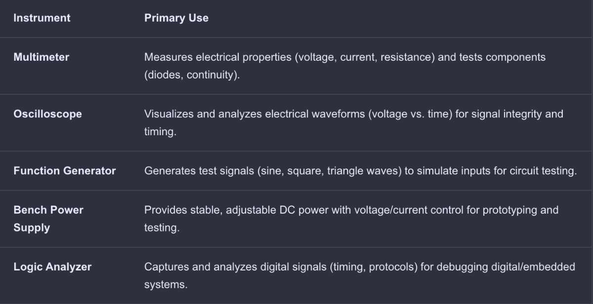 (AI Prompt: Differentiate between instruments used in the electronics lab *group page link*)
 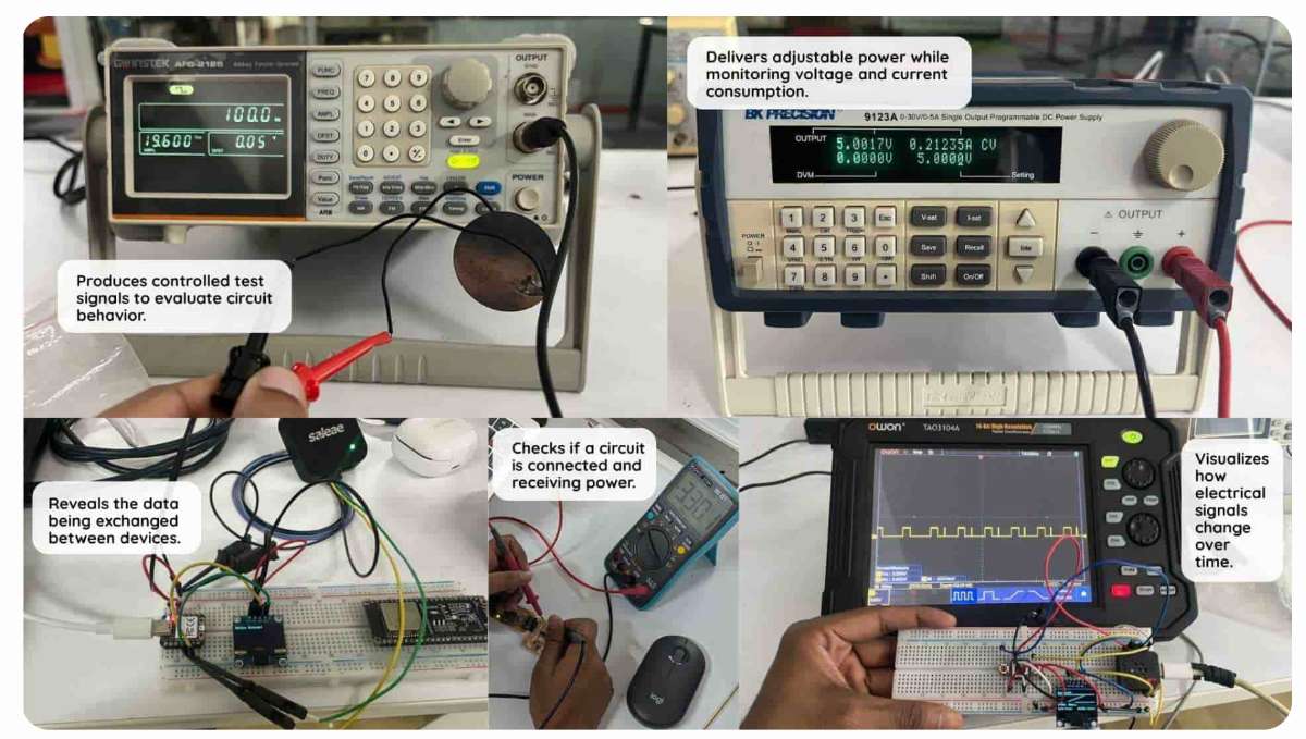 source
To know more, visit group assignment page
ELECTRONIC SIMULATION
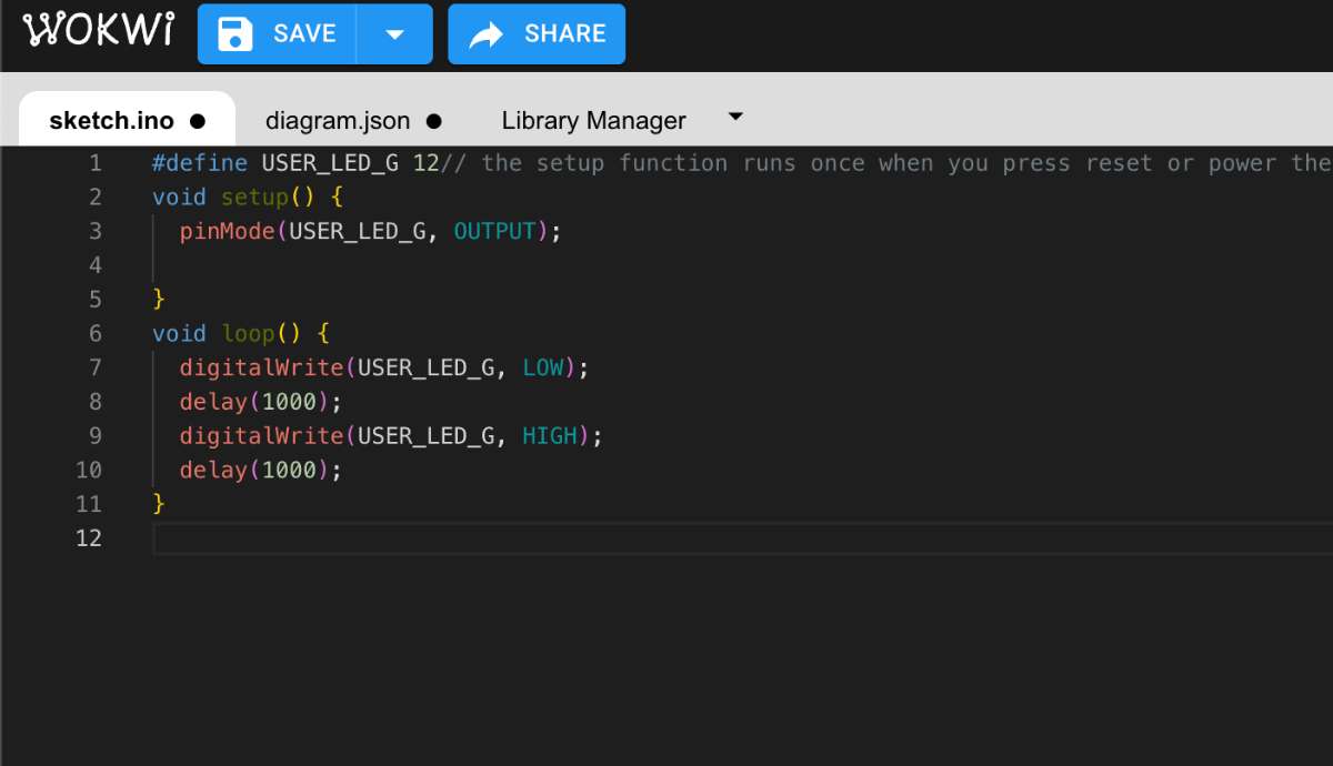
WOKWIWokwi is an online Electronics simulator. You can use it to simulate Arduino, ESP32, STM32, and many other popular boards, parts and sensors. I had previously worked on Raspberry Pi Pico using micropyton.
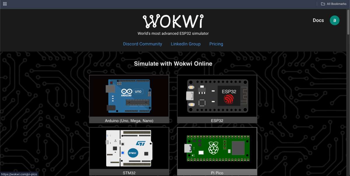 First, login to Wokwi, then i selected the Raspberry Pi Pico board and copy pasted the LED blinking code from the previous electronics week.
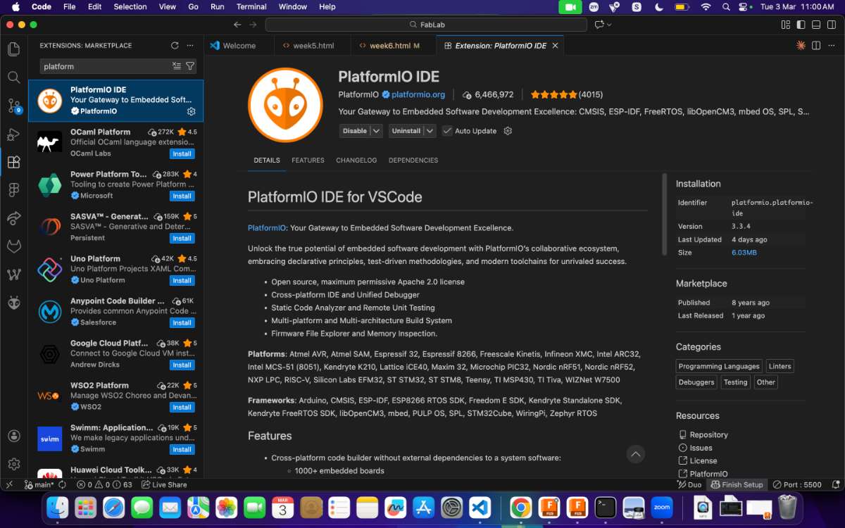
You can also run WOKWI locally, through your VScode using a PlatformIO plugin,Its a plugin for VS code and various IDE, a cross platform tool for embedding c++ development. Has advanced features and a debugger.
 To know more visit this Youtube Video
ELECTRONICS DESIGN
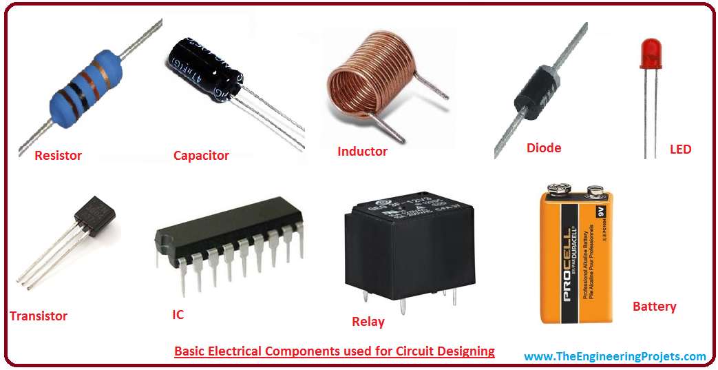
Electronic componentsElectronic components are the fundamental building blocks of electronic circuits, designed to control the flow of electricity in a system. They can be active (such as transistors and diodes) or passive (such as resistors and capacitors) , each serving a specific function within a circuit. When connected on a printed circuit board (PCB), these components work together to form functional electronic devices.
 source
 Active and passive components - Active and passive components are the two main types of electronic components used in circuits. Active components require an external power source to function and can amplify, switch, or generate electrical signals. Common examples include transistors, diodes, and operational amplifiers. In contrast, passive components do not need an external power source and mainly resist, store, or control the flow of electricity without amplification. Examples of passive components include resistors, capacitors, and inductors. Both active and passive components are essential for building and operating electronic circuits.
Resistor - A resistor is a passive electronic component that limits or regulates the flow of electric current in a circuit. It is commonly used to control voltage levels, divide currents, and protect components from excessive current.
Capacitor - A capacitor consists of two or more parallel conductive plates that are electrically separated by an insulating material called the dielectric. These plates do not touch each other, and the dielectric can be made of air, waxed paper, mica, ceramic, plastic, or a liquid gel (as found in electrolytic capacitors).
Inductor - is a passive electronic component that temporarily stores energy in a magnetic field when an electric current passes through its coil. It consists of two terminals and a coil of insulated wire, which can either loop through the air or wrap around a core material that strengthens the magnetic field. Inductors play a key role in managing fluctuations in electrical current within a circuit.
Transistor - is a semiconductor device that plays a vital role in amplifying or switching electronic signals and electrical power. It is composed of three layers of semiconductor material, where the flow of current or voltage between two layers is controlled by applying an electric current or voltage to the third layer.
Diode is a semiconductor device that primarily allows current to flow in one direction while blocking it in the opposite direction. This property makes diodes essential for converting alternating current (AC) to direct current (DC), protecting circuits, and enabling various electronic functions.Diodes operate in two modes:
Forward Bias: When the anode is at a higher potential than the cathode, the diode conducts electricity.
Reverse Bias: When the cathode is at a higher potential, the diode blocks current, acting as an insulator.
Types of Diodes
Rectifier Diode : Used for converting AC to DC.
Zener Diode : Designed to operate in reverse bias and regulate voltage.
Light Emitting Diode (LED) : Emits light when forward-biased.
Photodiode : Converts light into electrical current.
Integrated circuits (IC) Integrated circuits (ICs) are essential components in modern electronics, consisting of resistors, capacitors, inductors, diodes, and transistors fabricated onto a single semiconductor chip, usually made of silicon. These components are interconnected to perform specific functions such as amplification, signal processing, computation, and power management.
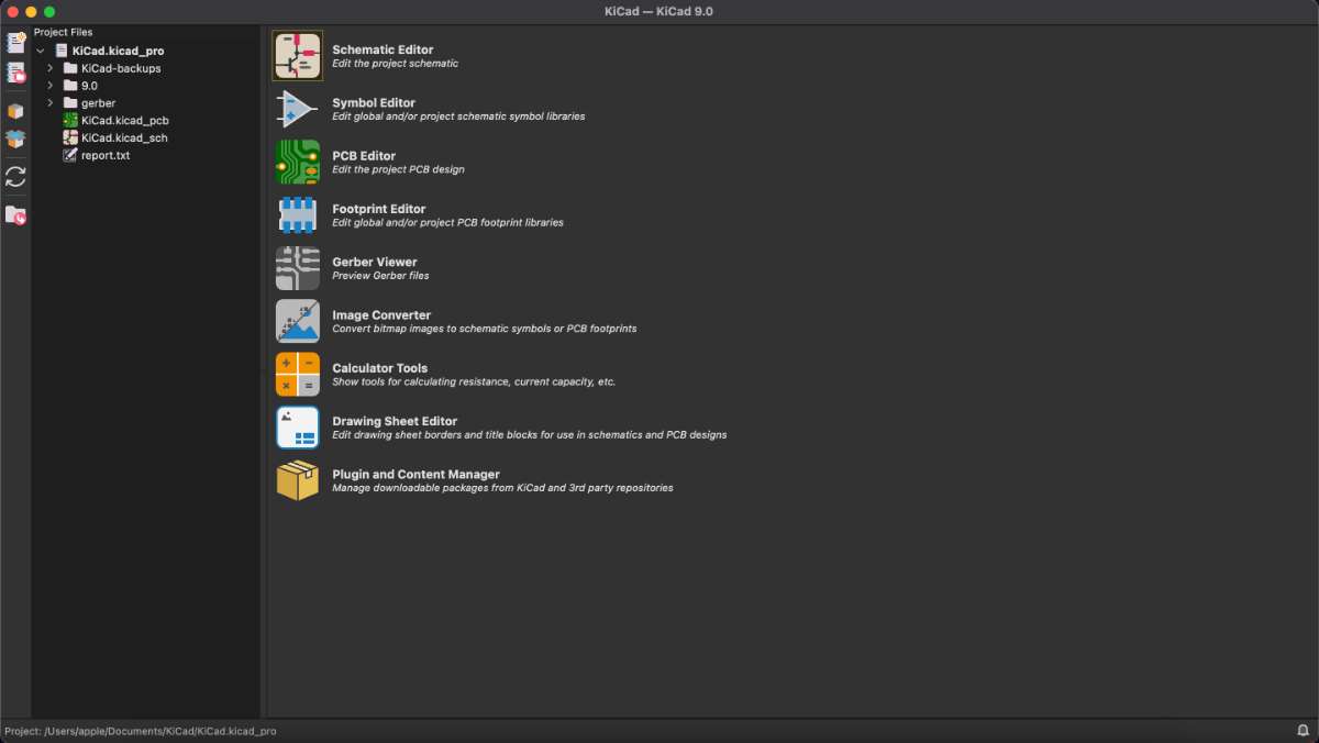
KiCad
KiCad is a free, open-source Electronic Design Automation (EDA) software suite used for creating schematics and designing printed circuit boards (PCBs). It provides tools for schematic capture, PCB layout, circuit simulation, and generating manufacturing files such as Gerber files. KiCad also includes features like 3D modeling, bill of materials (BOM) generation, and engineering calculations, making it a powerful tool for electronics design.
(Definition from Google AI, Prompt - Kicad Definition)
Go to the official KiCad website. Choose your operating system (Windows, macOS, or Linux). Download the installer for the latest stable version.Run the installer and follow the installation instructions.I downloaded and installed KiCad. Now open KiCad . File -> New Project -> Name your project
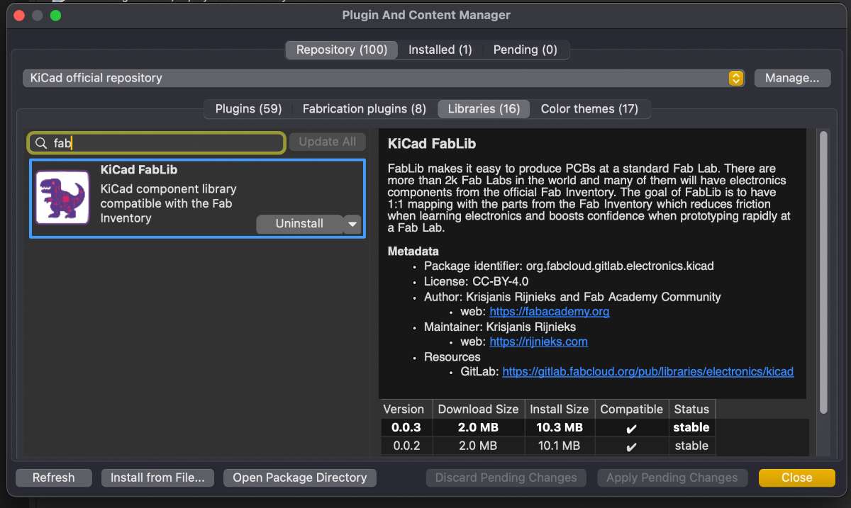
 Using the FabLab Library in KiCad
To add git lab KiCad Library
(Step 1): Go to "Tools > Plugin and Content Manager" or press Ctrl + M.
(Step 2): Select the Libraries tab.
(Step 3): Look for "KiCad FabLib" in the "Libraries" tab.
(Step 4): Click "Install".
(Step 5): Click "Apply Pending Changes".
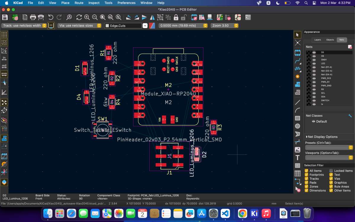
 Pinout of XIAO RP2040
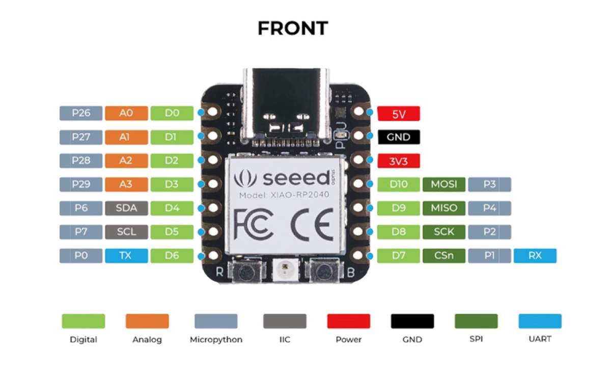 source
 Schematic Editor
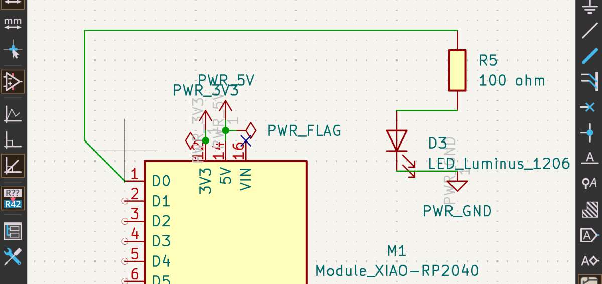
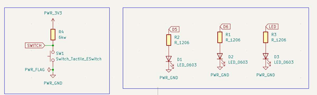
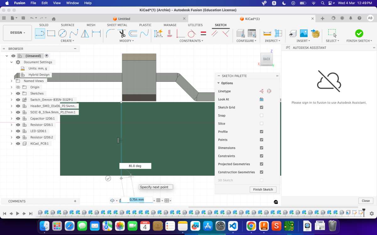
I used XiaoRP2040 microcontroller to build the PCB, Firt you start by adding the component. Press A or click the "Place Symbol" tool.
Search for the component
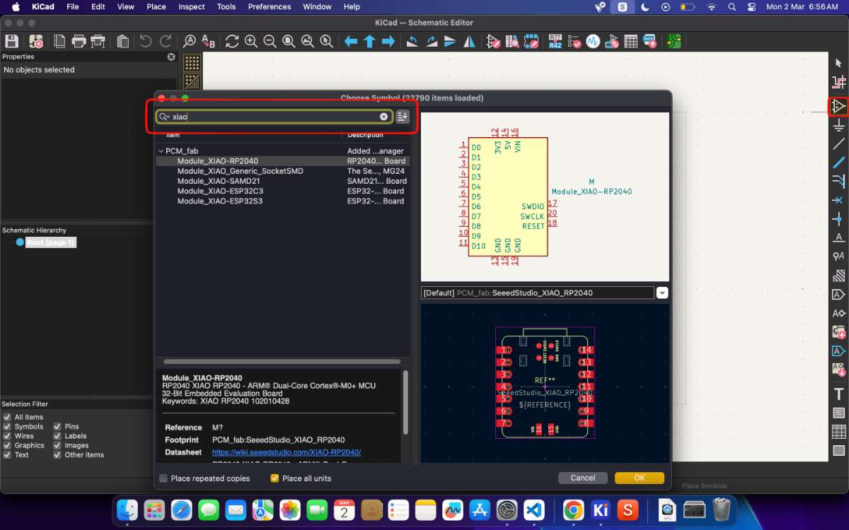 Click to place it on the canvas. Now, you can add the remaining various components such as the power, LEDs, switch, resistor, capacitor etc . and then
marking the PINs of the XIAO, The Serial Clock Pin (SCL) and the Serial Data Pin (SDC) pins are used in I2C protocol. The SCL pin sets the speed of
data transfer, while SDC pin tranfers the data. An example where I2C is used is in OLED screens.
Click to place it on the canvas. Now, you can add the remaining various components such as the power, LEDs, switch, resistor, capacitor etc . and then
marking the PINs of the XIAO, The Serial Clock Pin (SCL) and the Serial Data Pin (SDC) pins are used in I2C protocol. The SCL pin sets the speed of
data transfer, while SDC pin tranfers the data. An example where I2C is used is in OLED screens. Adding an external component using SnapMagic
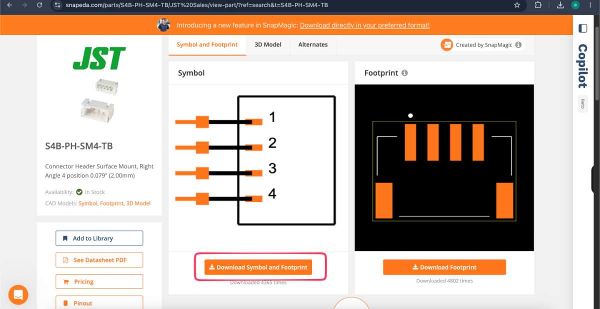
One of the goals this week was to learn how to find and bring in a component that is not in the KiCad Fab library. You can you can import it from SnapMagic, a free online library of symbols, footprints, and 3D models. PS: This is also why my production week board differs slightly from the version I made in this week — I added this JST connector afterwards in the production week.
I am recording my steps here:
- Searched for the 4-pin JST connector on the SnapMagic website and opened its page.
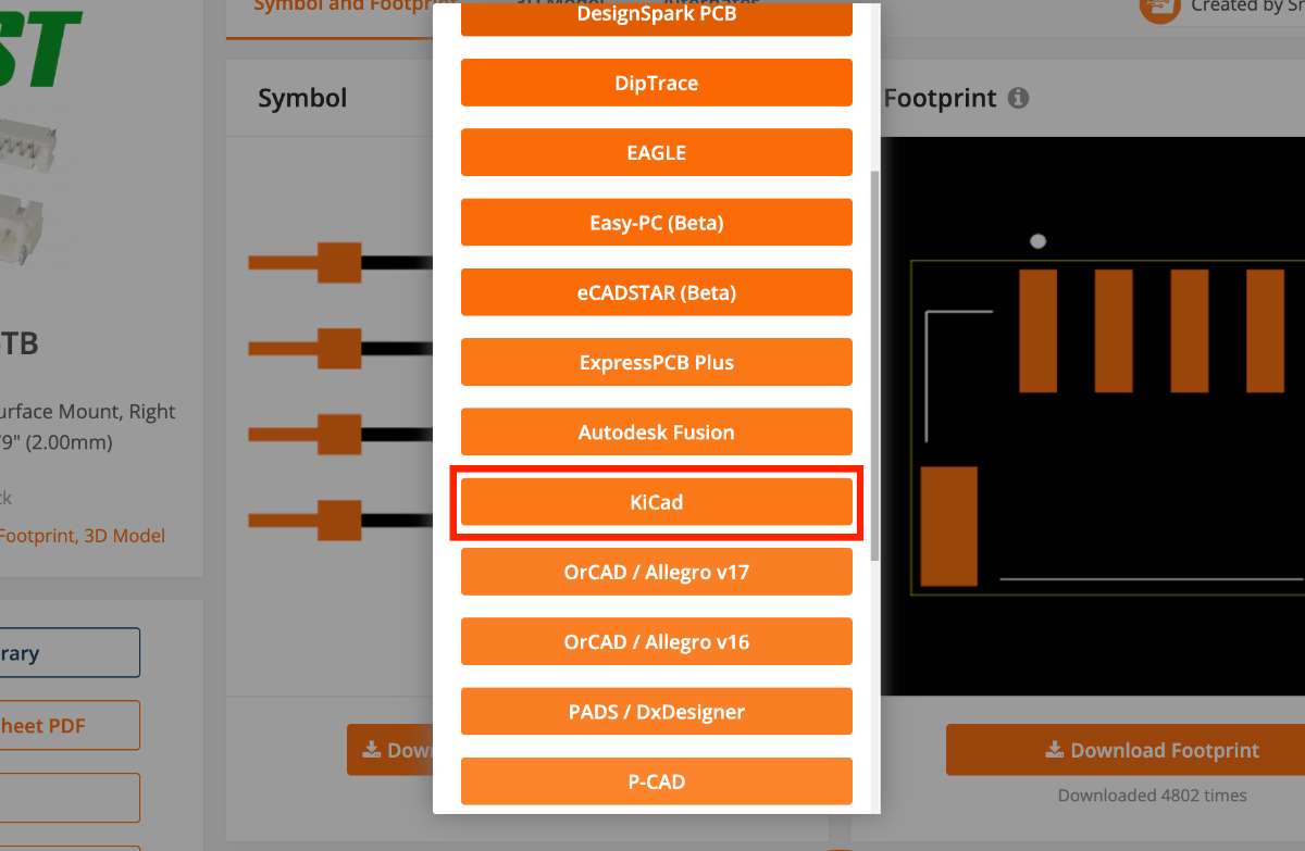
- Chose Download → KiCad format (this gives a symbol
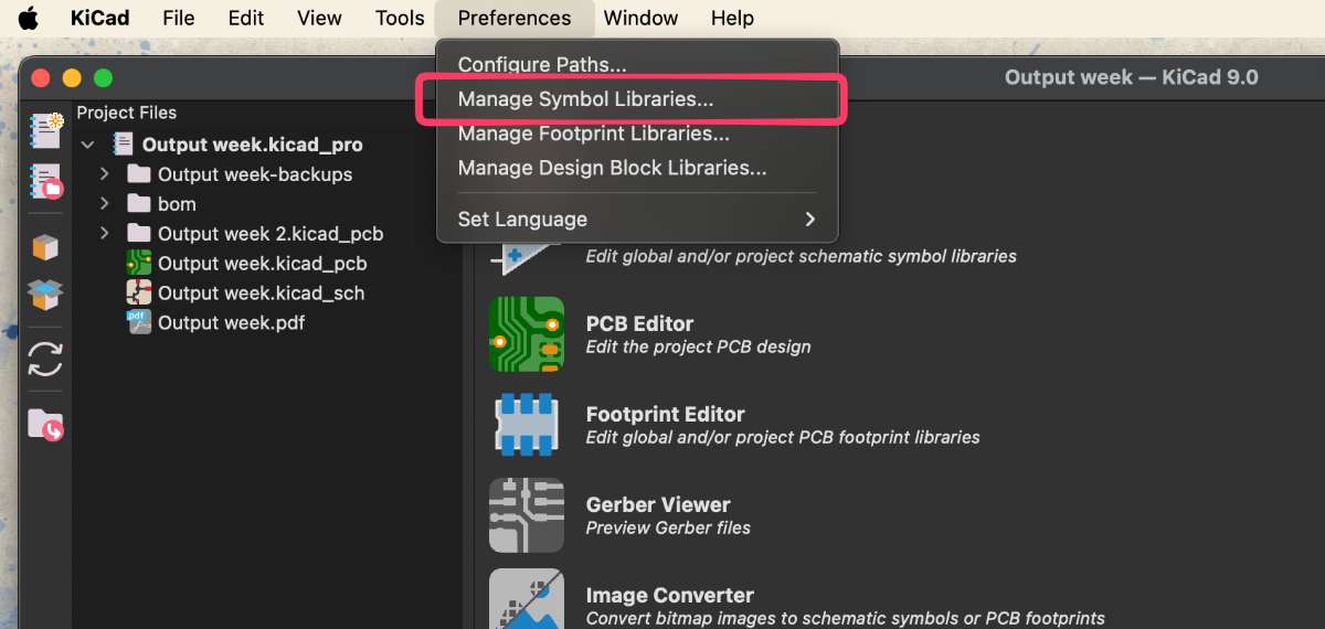
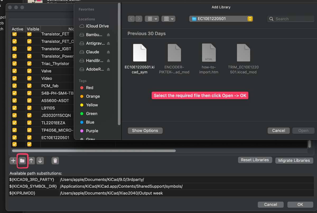
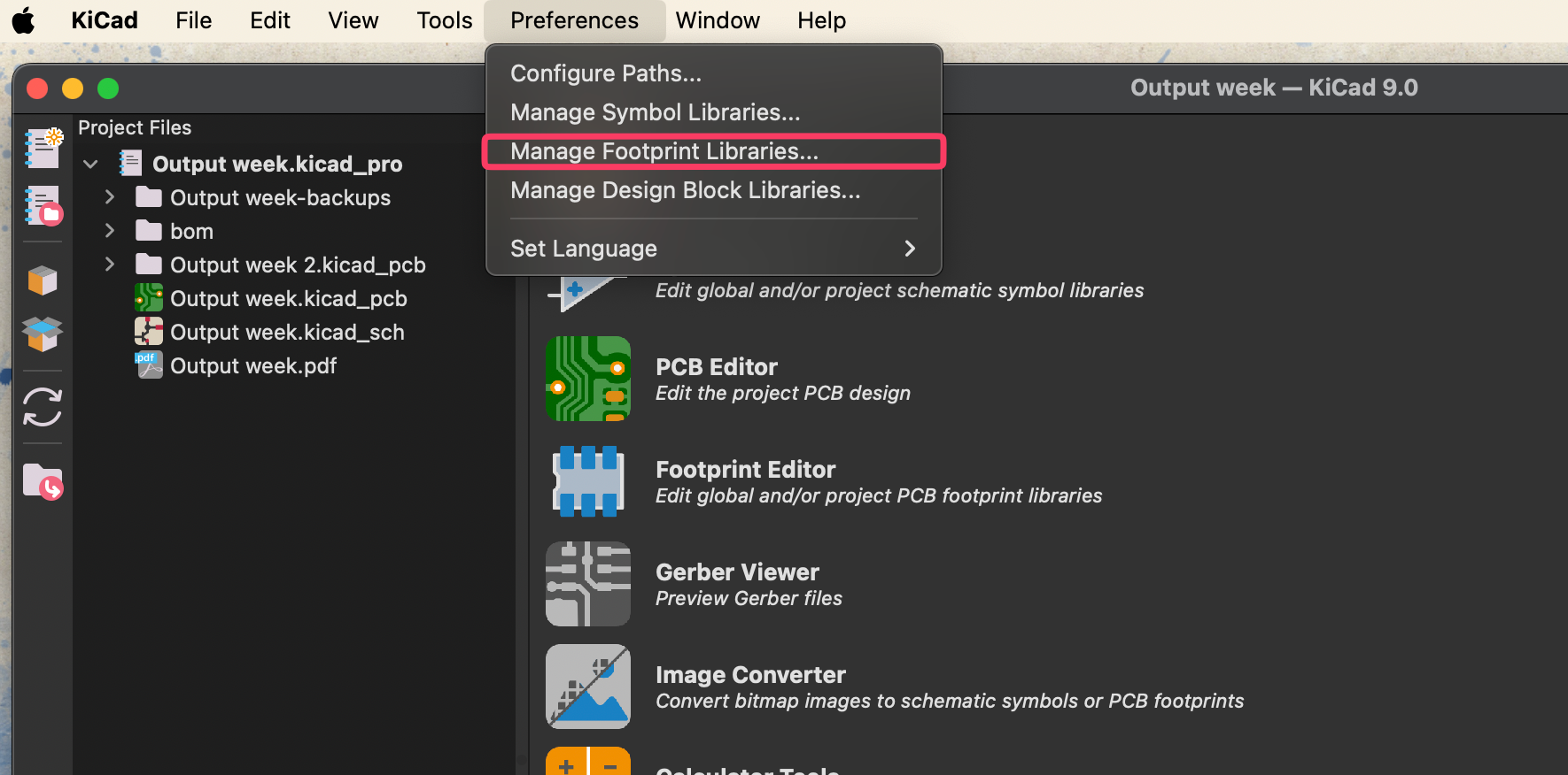
.lib/.kicad_sym, a footprint.kicad_mod, and a 3D model). - In KiCad, opened Preferences → Manage Symbol Libraries and added the downloaded symbol file as a new library.
- Opened Preferences → Manage Footprint Libraries and added the downloaded footprint folder the same way.
- Back in the schematic I pressed A, searched for the new connector, and placed it. The footprint was already linked, so it carried straight through to the PCB.
Labeling and wiring
Instead of running a wire across the whole sheet for every connection like the following image :
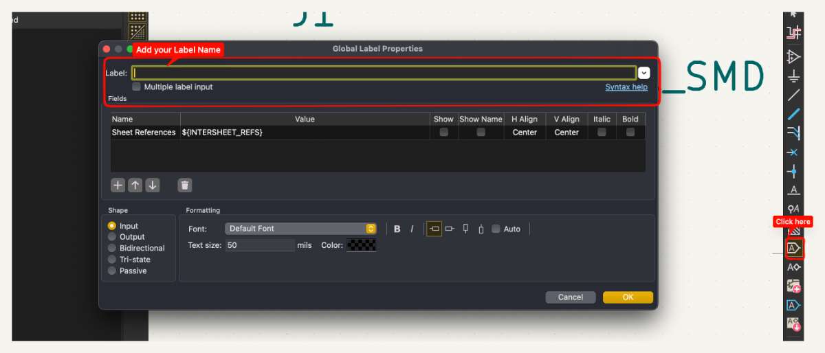
 I used labels.
You draw a short wire stub off a pin, then press L (or pick "Place Net Label" from the right
toolbar) and type a name. Any two stubs that share the same label name are treated as electrically connected,
even though there is no visible wire between them.
I used labels.
You draw a short wire stub off a pin, then press L (or pick "Place Net Label" from the right
toolbar) and type a name. Any two stubs that share the same label name are treated as electrically connected,
even though there is no visible wire between them.
Why labels instead of wires:
- The canvas stays clean, no long wires crossing over each other and getting hard to read.
- Fewer accidental junctions, so it is easier to see what is actually connected.
- It is faster to change a connection: rename a label instead of deleting and redrawing wires.
How I did the pin labeling: I hovered over the pin I wanted to name, drew a small wire,
pressed L, typed the net name (for example SDA, SCL and placed it on the stub. I repeated the same name on the matching pin elsewhere.
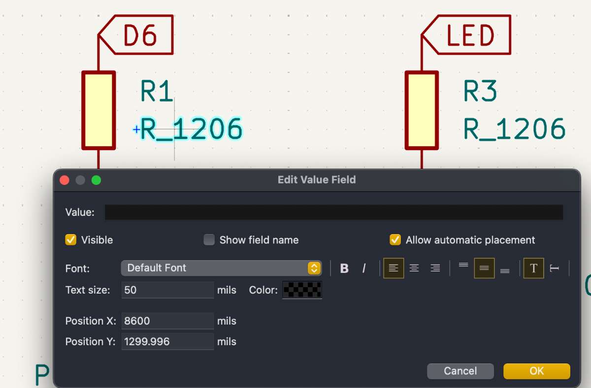
Press E while hovering over a component(or double click at the value) to edit its value (e.g., 220 Ω for a resistor).
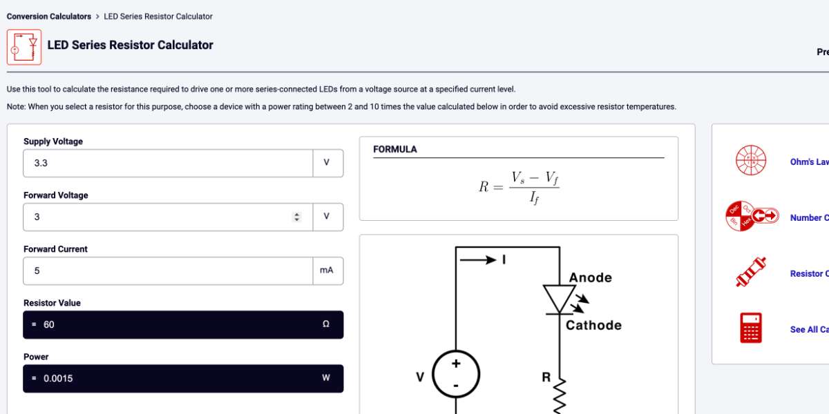
Choosing the LED resistor value
I didn't pick the resistor randomly To double check I also used an online through the
LED resistor calculator — you enter
the supply voltage, the LED forward voltage, and the desired current, and it gives you the resistor value. The value i got it 60ohms but since my lab did not have that i used the next big value present which was 100 ohm.
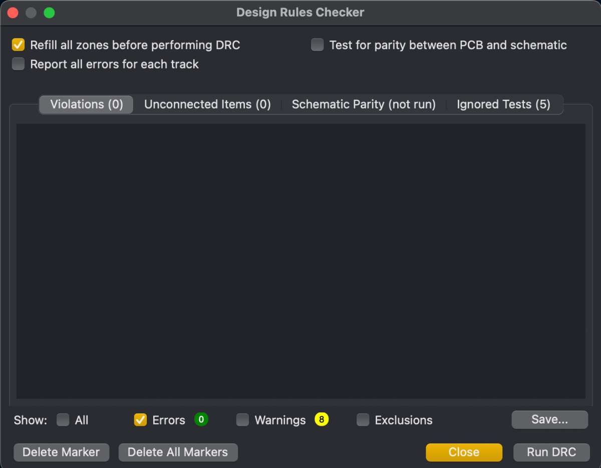
Electrical Rule Check (ERC)
After that we can perform Electrical Rule Check (ERC) it is an automated verification tool in the Schematic Editor that
scans your circuit design for electrical, connectivity, and, logical errors. From the top tool bar click Inspect -> Run
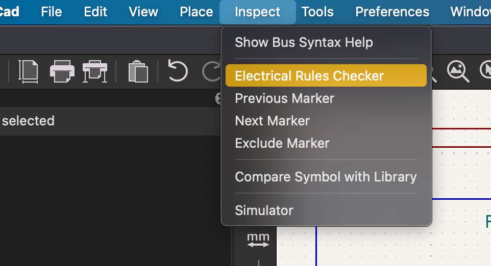
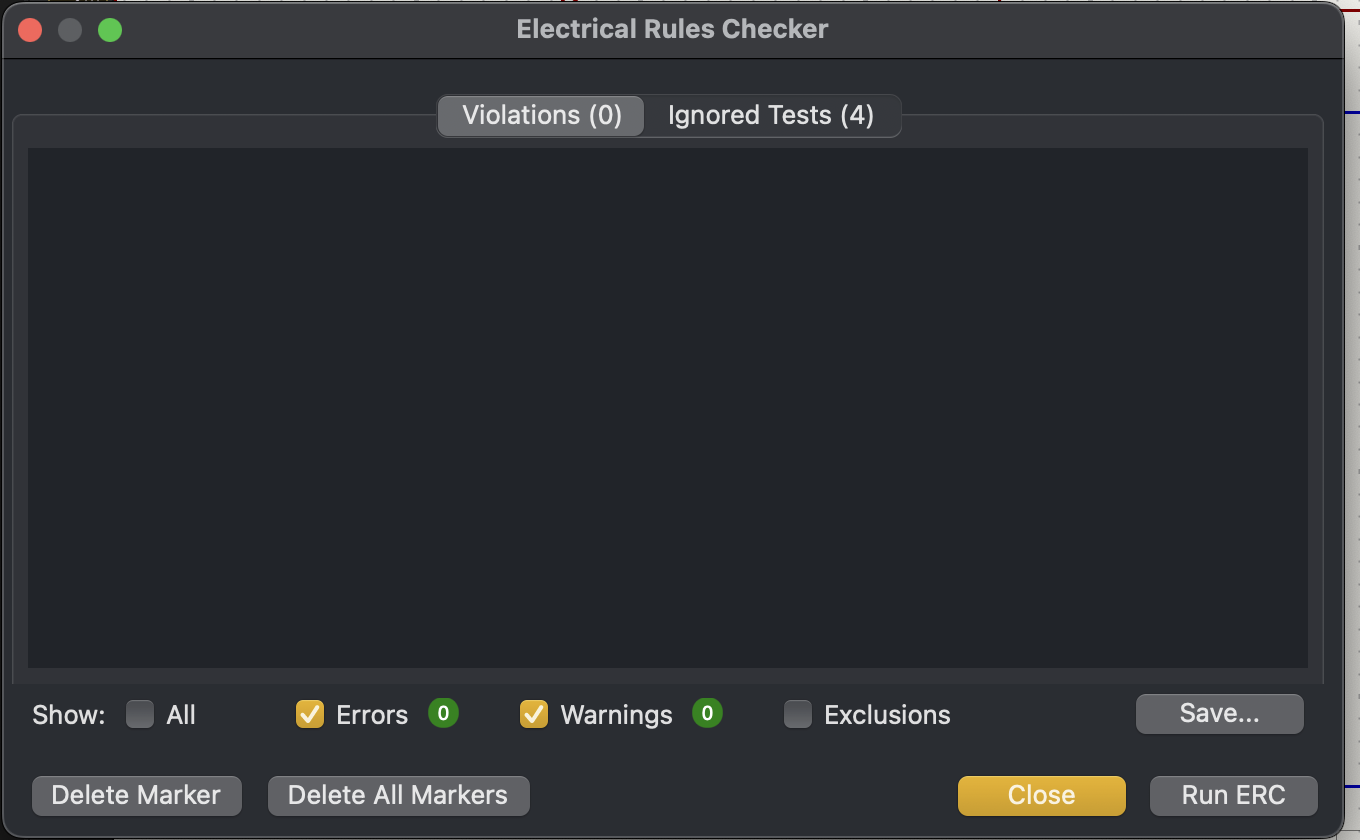
Here, i do not have any violations or errors.
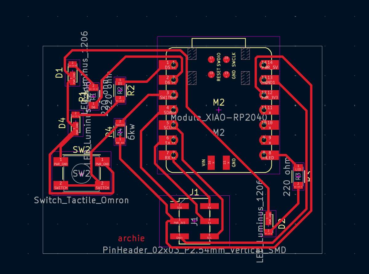
To keep the schematic readable I grouped related parts together I drew boxes and lines around each block using the graphic rectangle and line tools (the "Draw rectangles" / "Draw lines" buttons on the right toolbar).
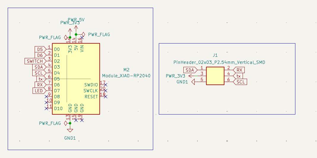
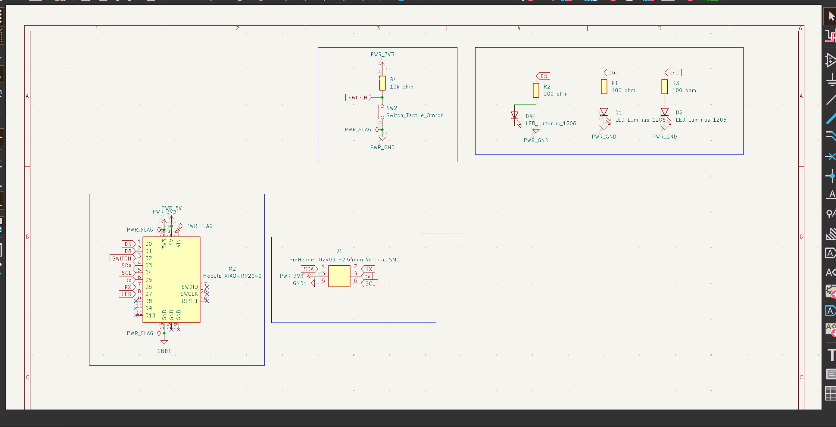 Above i have connected by label instead of Wire(Press W or click the "Place Wire" tool) from the right tool bar.
 PCB LAYOUT
In the top toolbar click the following icon -> run .
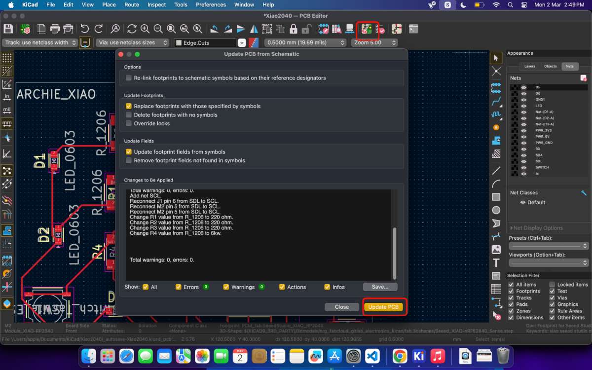 Now we need to place each component in such a way to reduce the number of knotted airwires.
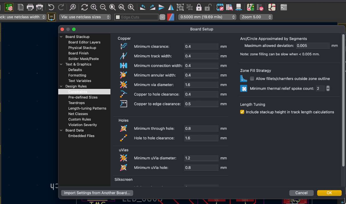
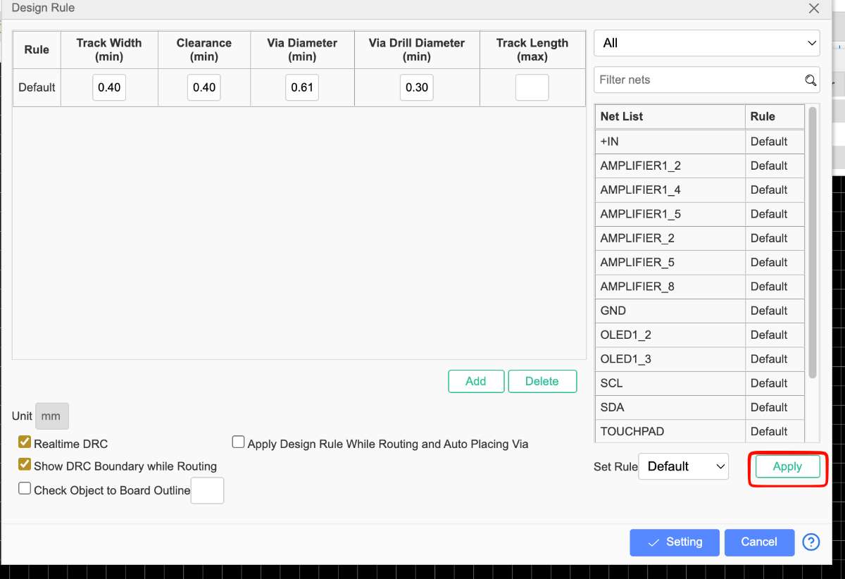
Design rules / Board Setup (tracing constraints)
Before routing I set the trace and clearance constraints under File → Board Setup → Design Rules → Constraints / Net Classes. My instructor gave me these values so that the tracks would survive our lab's fabrication process — if the traces are too thin or too close together the milling/etching can't reproduce them reliably. The screenshot below shows the values I entered.
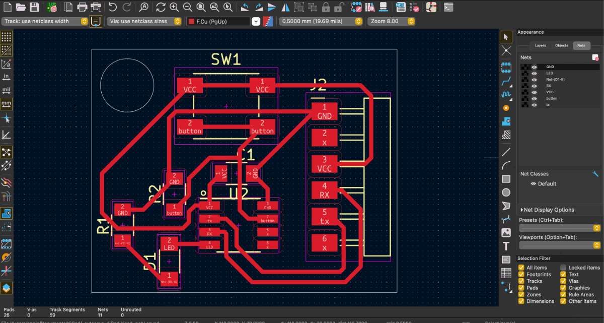
 Once placement is done, its time to draw traces.
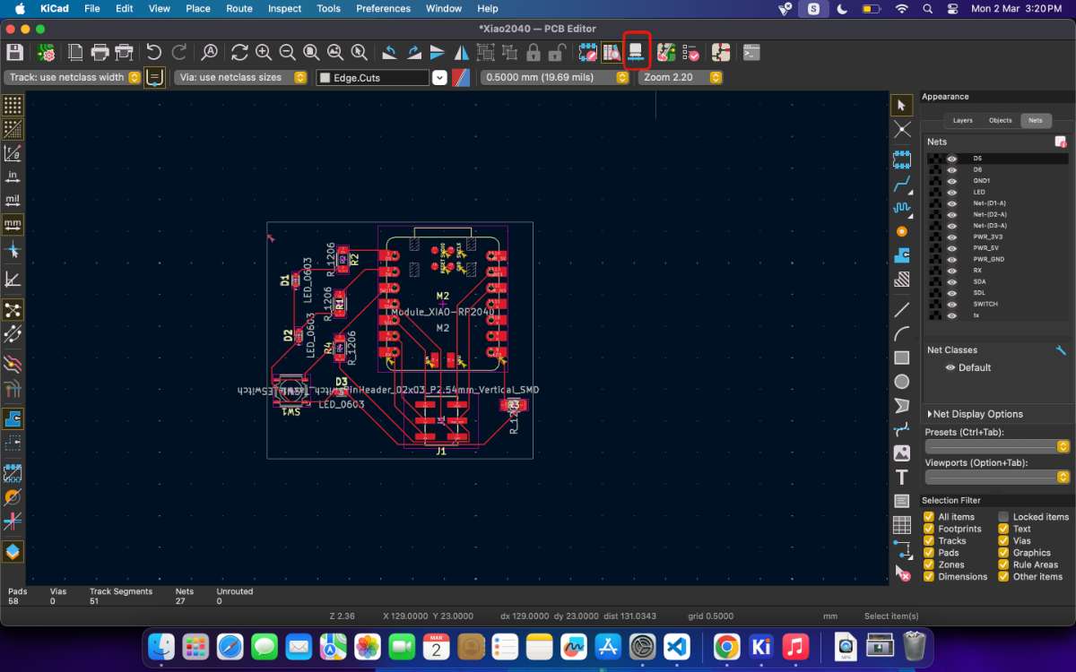
To connect two pads I did the following:
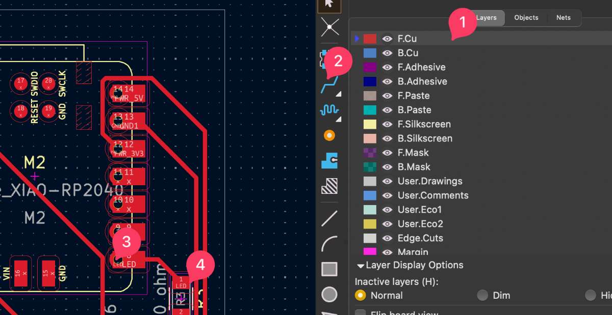
- Selected the F.Cu (front copper) layer from the layers panel.
- Pressed X (Route Tracks) to start a trace.
- Clicked the first pad, moved to the second pad following the airwire guide, and clicked to finish.
- Used the tilde (~) key to highlight all connections of a terminal, and D to drag/edit a path when I needed to reroute around another track.
- Routed signal tracks first and left ground and power for last.
Only traces for ground and power at the last, after all other connections have been made.
Avoid 90 degrees in traces, add cruves using D command
Using tilde key to see all connections of one terminal
Using D to edit traced paths
select the trace and press U to select an entire traced path
Then i proceeded to draw an edge cut rectangle path (White colour).
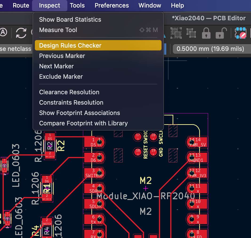
DRC Check
Next i did Design Rule Check (DRC), it s an automated tool within the PCB Editor that verifies a layout against predefined electrical and physical constraints.
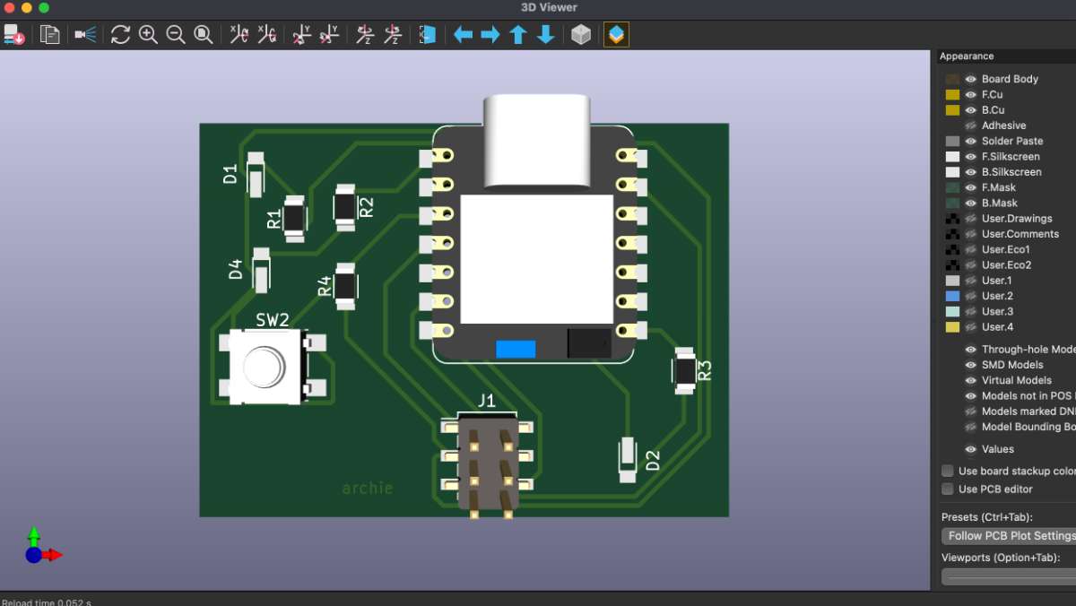
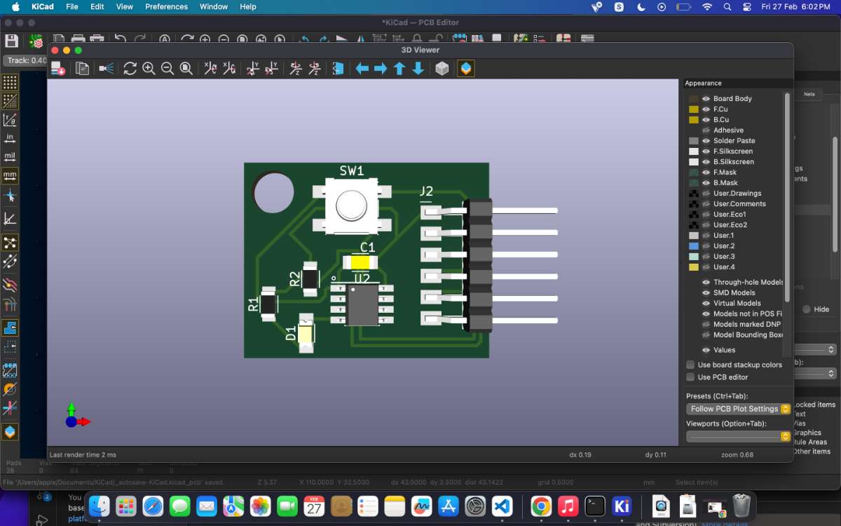
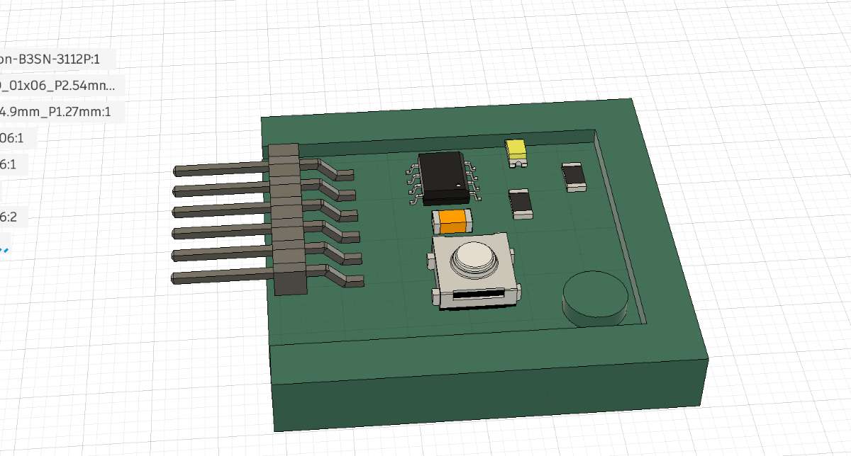
 Viewing in 3D
Now moving to the third part of the designing process; 3D models.
 This is the final result.
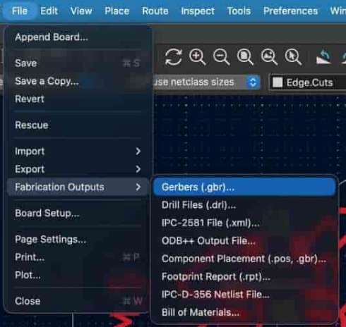
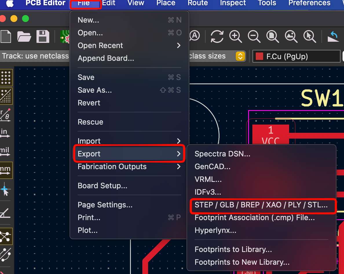
 What are Gerber files?
Gerber files are the standard manufacturing files used by PCB factories to fabricate your board. They describe each physical layer of the PCB (copper, solder mask, silkscreen, board outline, etc.).
Export in Gerber:
Open File → Gabrication Outputs → Gerber .gbr
 to view the gerber file use
gerber2png website
to view the gerber file use
gerber2png websiteATtiny412 PCB Design
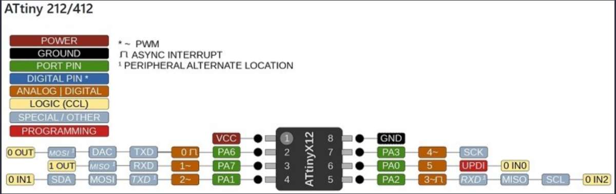 source
We made a PCB using ATtiny412 microcontroller, Our instructor said it was for "training" purposes, and we made it before the XiaoRP2040.
I made the connection diagram in schematic editor
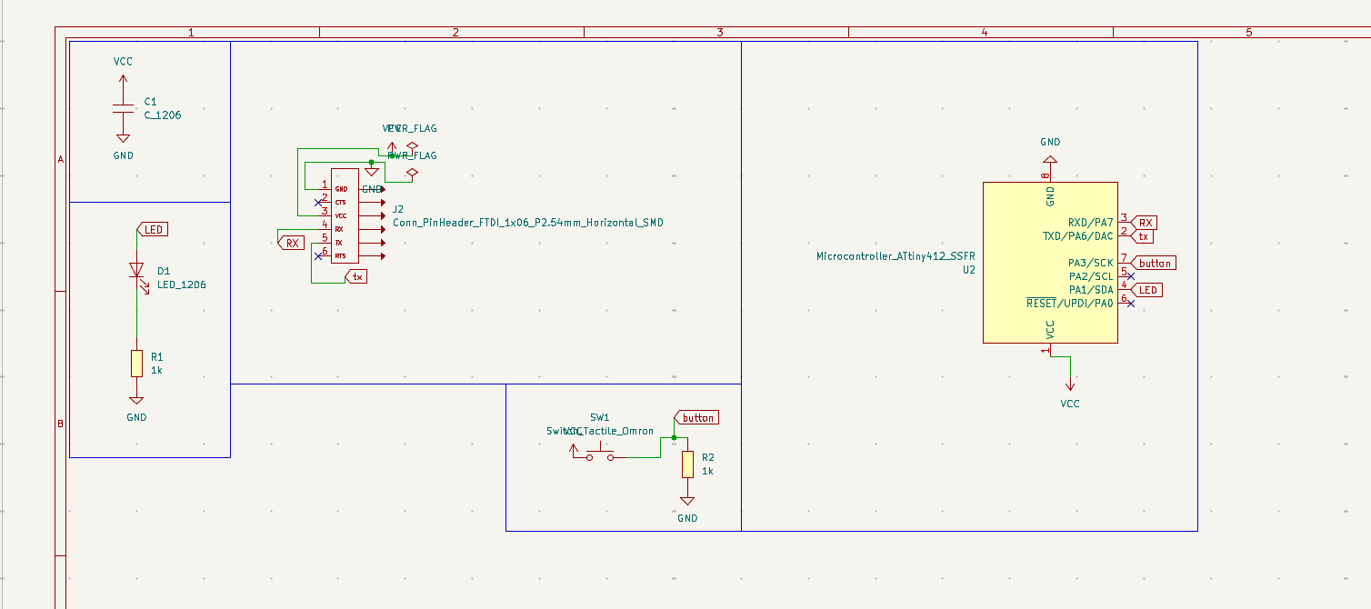 Then I followed the same workflow: component placement, routing, DRC, and 3D preview.
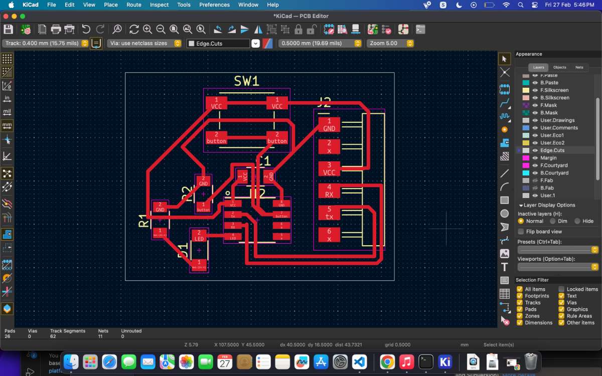 after the review i got a feedback to change the traces in such a way that it shouldn't be 90 degrees, because it might lead to acid deposition.
 Final Output:
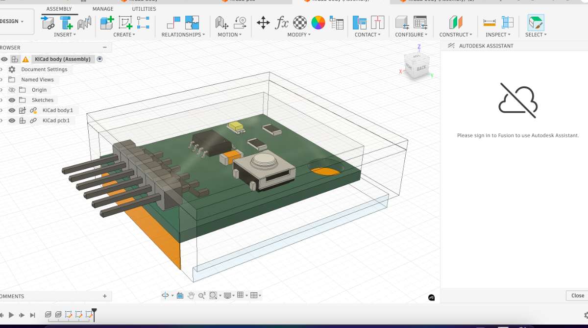
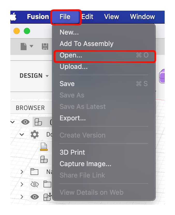
 PCB Case design in Fusion 360
First Export the file in STEP format from KiCAD:
 Then open in to open in fusion , go to file->open
 After exporting i extended the border using shell function.
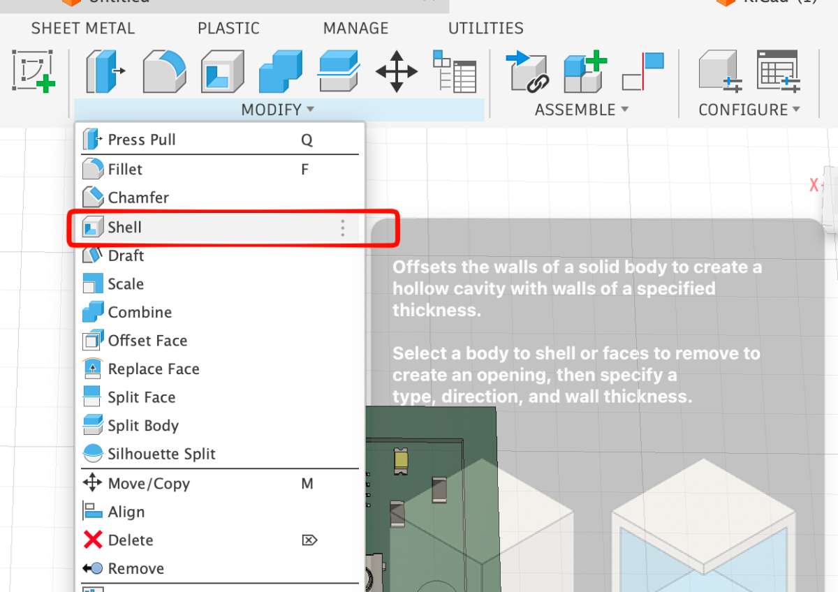 Then i drew a line and using the extrude key i cut the left portion off as it was sticking out a bit.
 To change appearance, go to modify-> choose which material you want.
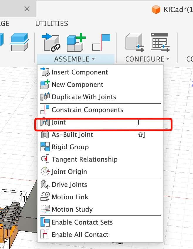
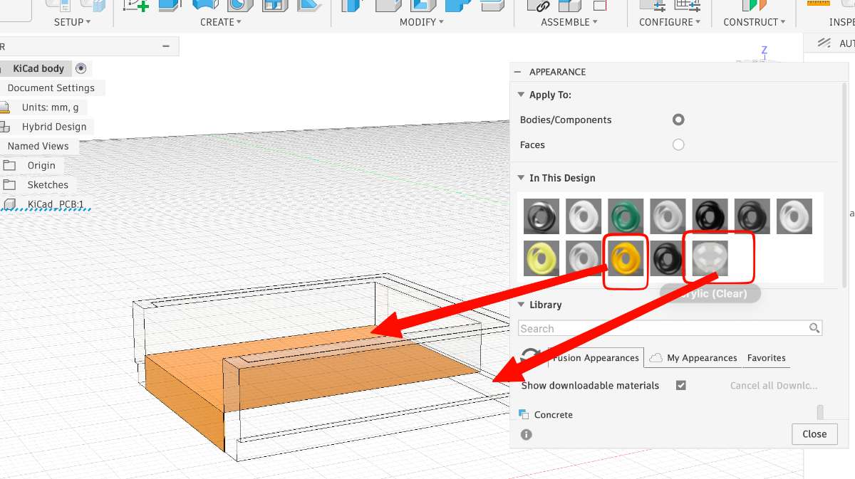 For the top portion i constructed an offset plane and drew a box there, then extruded it to my likimg. and then used the joint function to make the enclosure
 After changing the appearance , this is the following is the final output:
Snap EDA Plugin in FUSION 360
After changing the appearance , this is the following is the final output:
Snap EDA Plugin in FUSION 360What is Snap EDA?
Snap EDA is a lifesaver, it is a library for electronics design,which provides free, ready-to-use CAD models like schematic symbols, PCB footprints, and 3D models.
Now why use it?
quickly import electronic components into Fusion so you don’t have to build symbols, footprints, and 3D models from scratch.
How to get Snap EDA ?
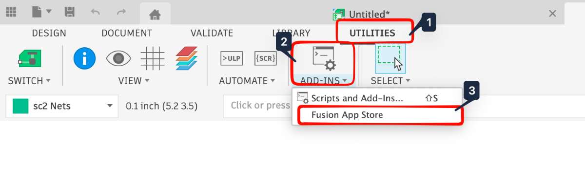
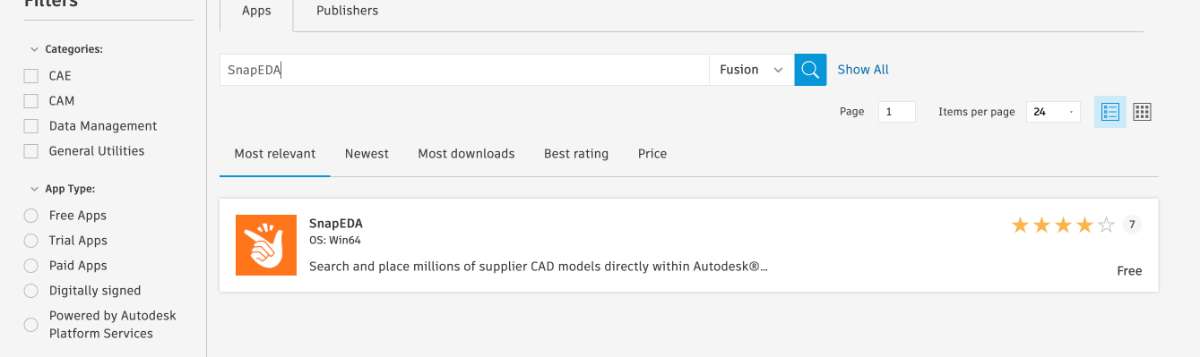
Open FUSION 360 & choose electronics tab, then click on the following icon.
 next you can add SnapDA to your Fusion, got o Utilities -> add ins -> Fusion apps -> search -> download(referYoutube Video)
 Now your Plugin is insatlled.
ok so apparently this is not supported in MacOS, i learnt that after spending hours on figuring out why i was not able to access the SnapEDA Though this website seemed to have info, the latest update of Fusion 360 did not support it. Sad. But for windows this(the plugin) works just fine.
Update: Easy EDA does work on Fusion but it took a day to show up on the toolbar, i am not sure why that happened, only noticed it on wood working week.
PCB Design - EasyEDA(Final Project Ed)
What ia EASY EDA?
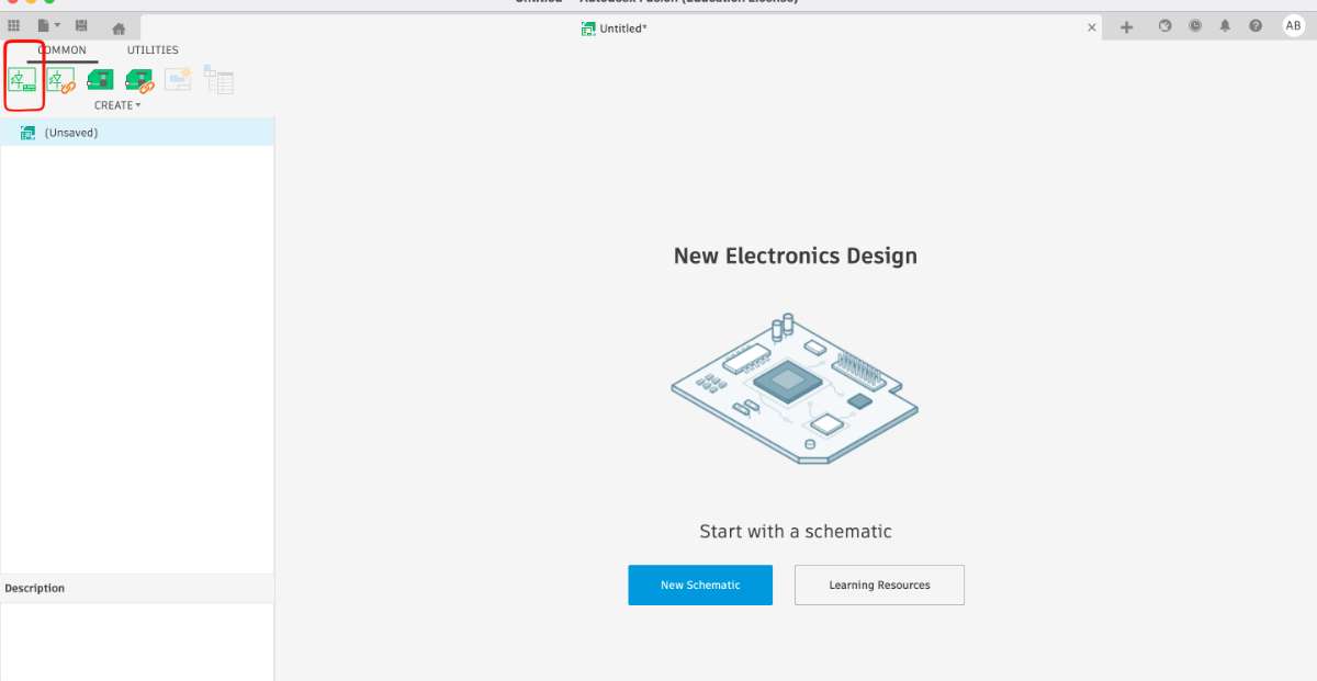
Easy EDA is a web-based electronics design software used to design schematics and printed circuit boards (PCBs). It runs directly in a browser and is widely used by hobbyists, students, and engineers because it is free and easy to start with. Go through the Website to know more.
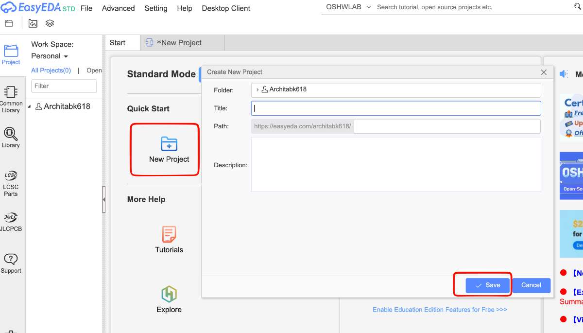
Go to Easy EDA website, click on new project and save your file.
 Then click on library->search for the component you are looking for.(xiao)
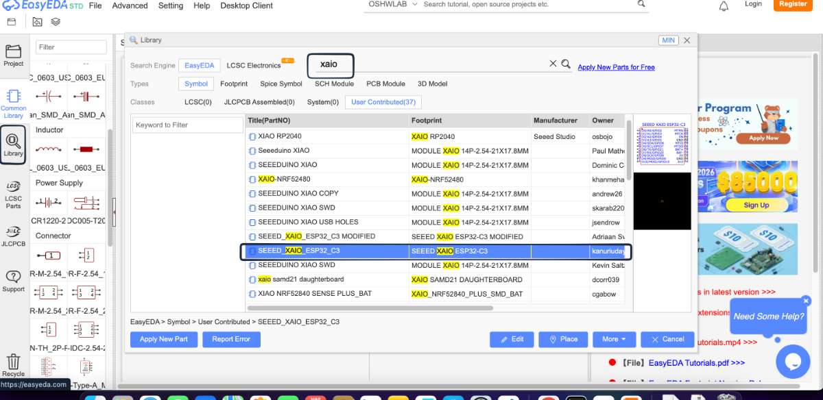
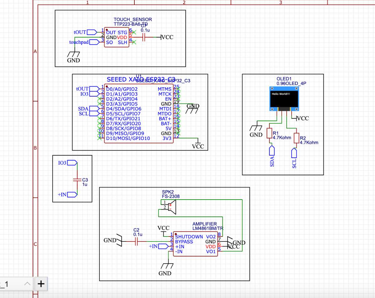
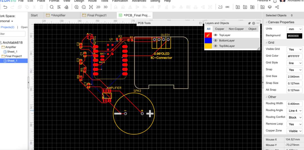
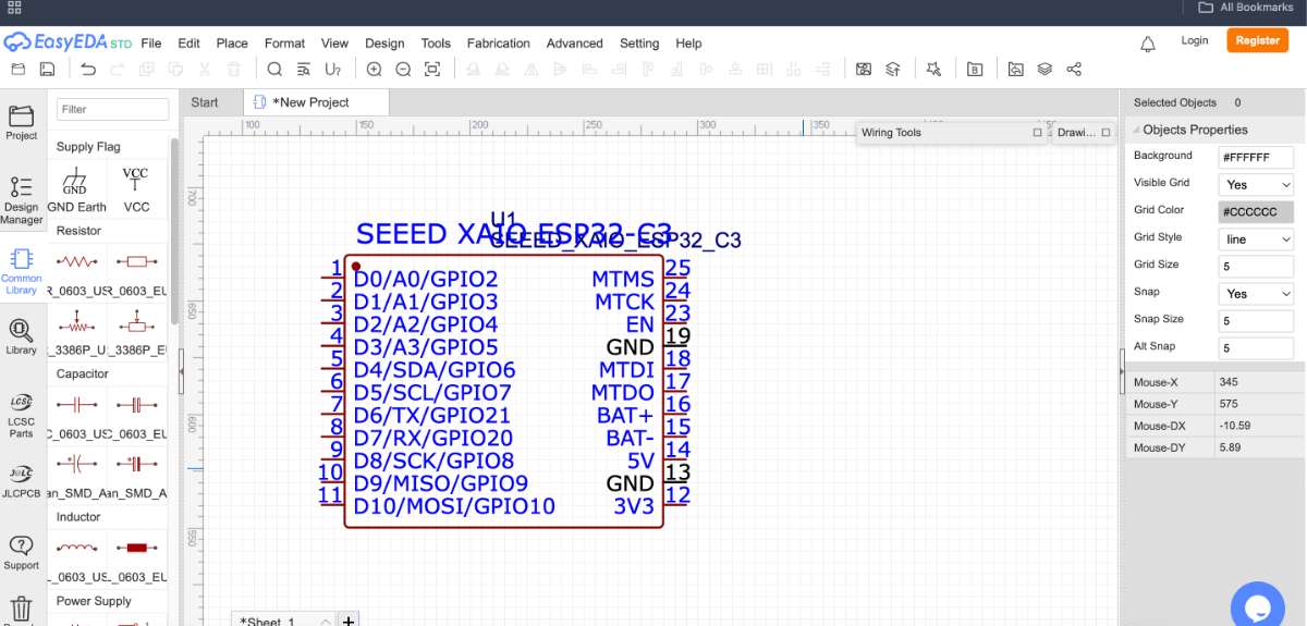 Follow the same steps and assemble the parts you want. Here, i have taken an amplifier, OLED screen, Speaker, Touch Sensor.
 I had a basic idea of what all the components were that i needed for my final project. But i didnt know how to connect or what all nittygrittys i was missing, So i asked Chat GPT ,
PROMPT: Give a **clear circuit diagram layout (**for my final project using the components
Seeed XIAO ESP32-C3,TP223 touch sensor*,0.96" I²C OLED,LM4861 audio amplifier,Speaker
and this gave me an almostclear idea of what steps i had to follow . Here is how the schematic looked after all of it.
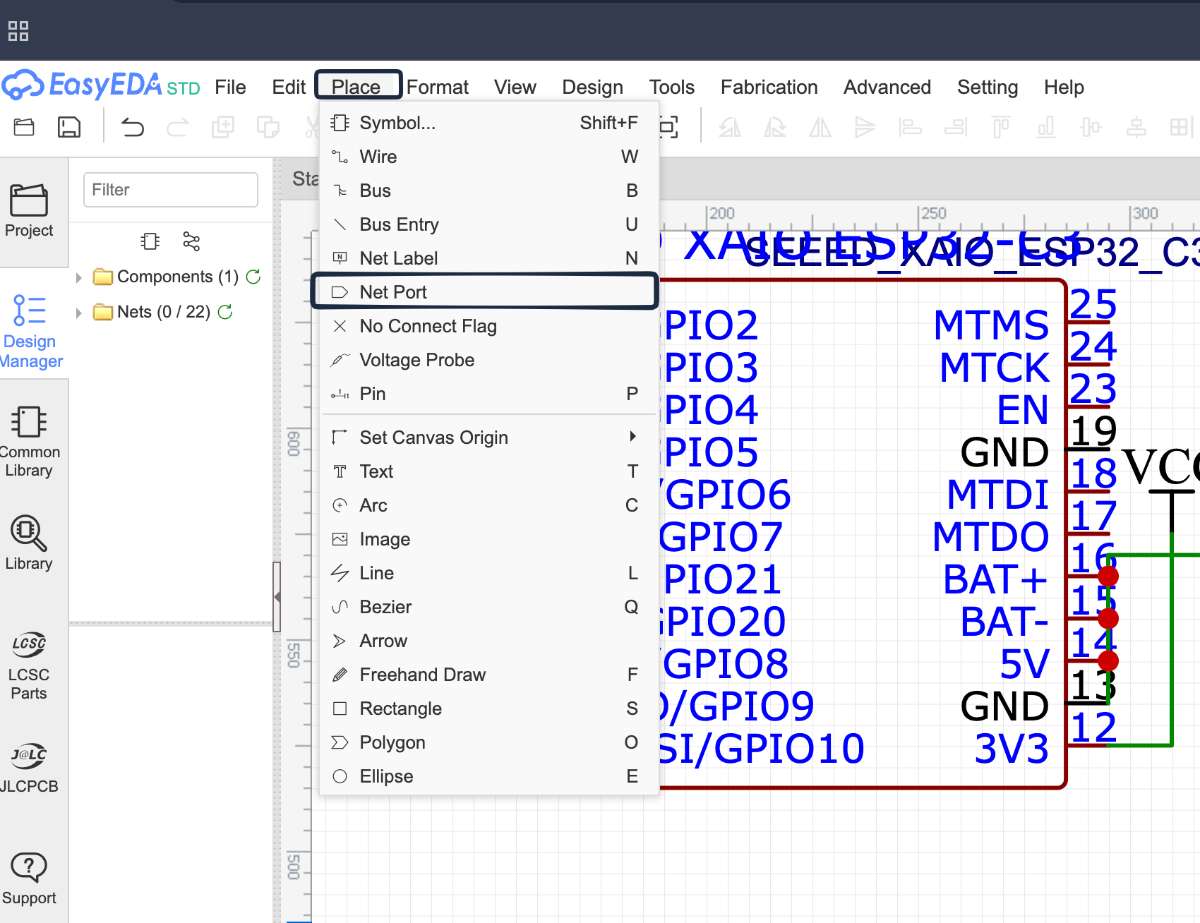
 To access the port labels go to the top tool bar & follow the steps shown in the following image:
 To cut the ports/pins not in use, go to the top tool bar & follow the steps shown in the following image:
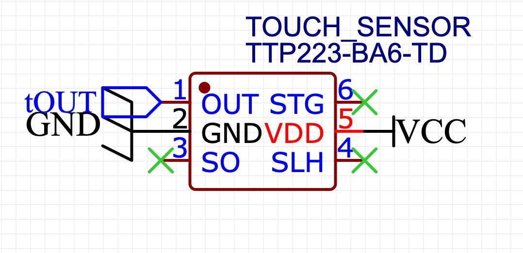
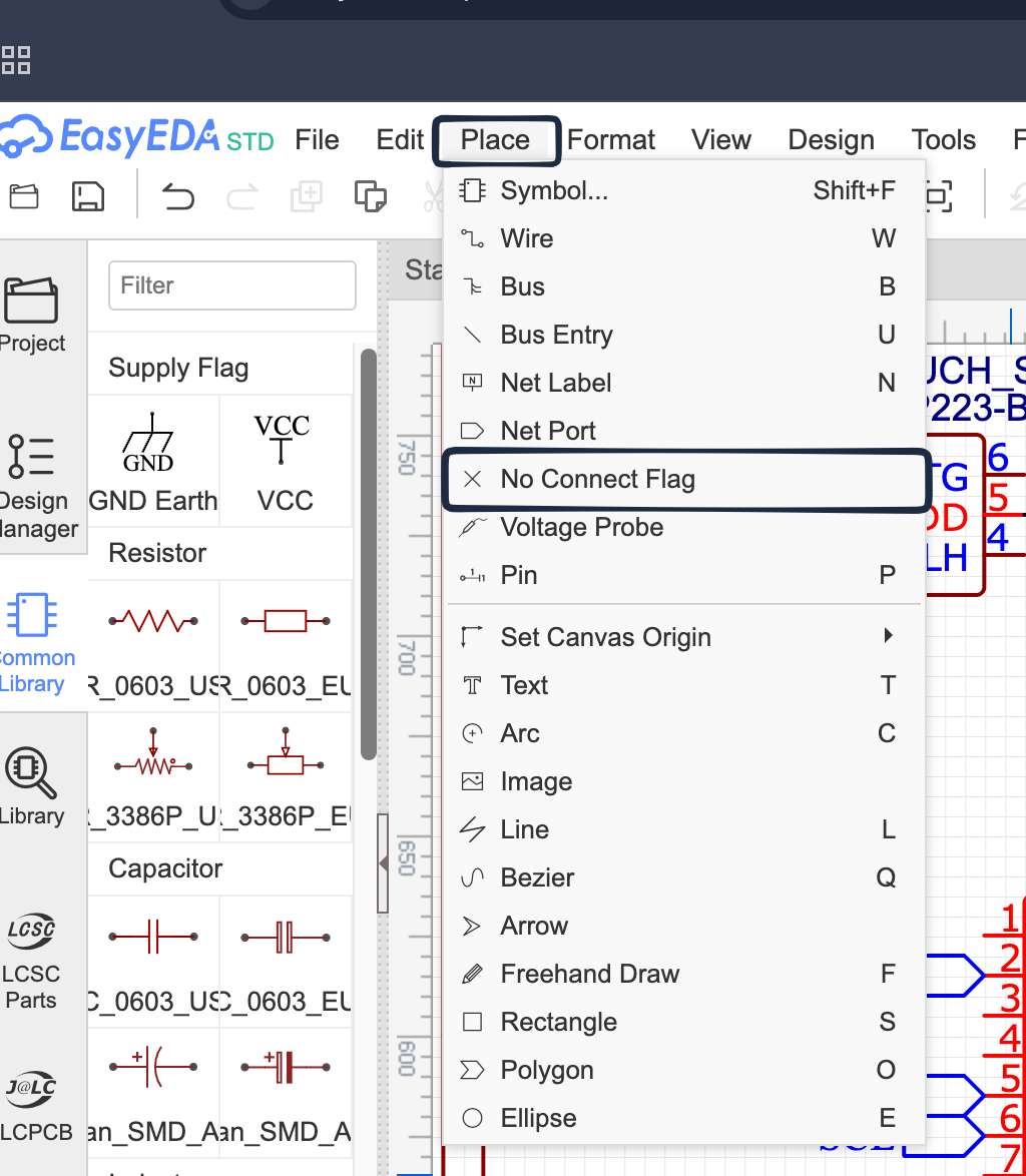 After selecting place the cross on the ports that are not in use
 After that click on design in the top tool bar and go to Convert to PCB:
 then to set the design settings:
 enter the measurements
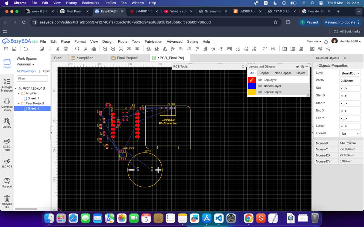
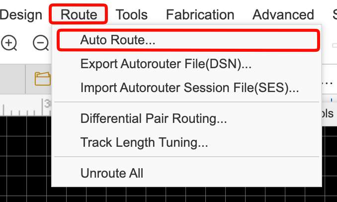
 After setting the required measurements and re arranging the components in a suitable way, trace it using auto trace:
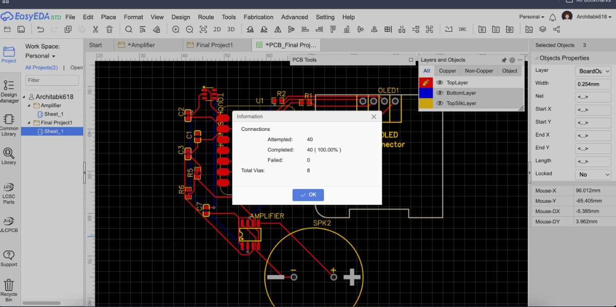 This is how the wiring looks:
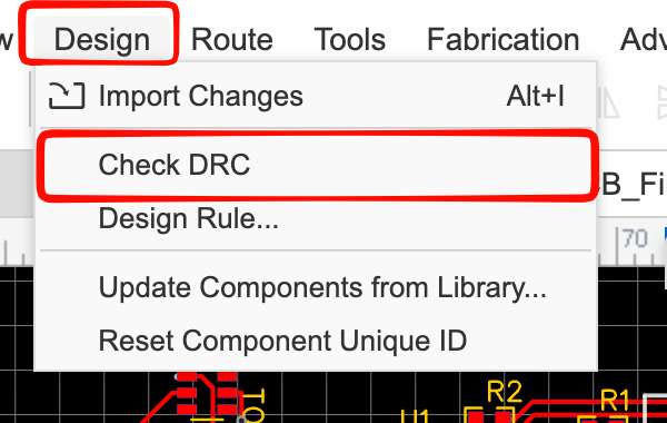
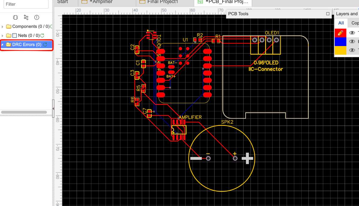
 Now to check for errors:
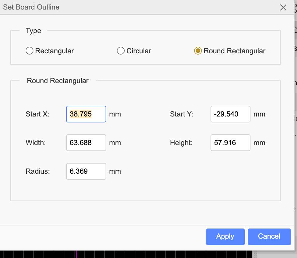
 from the top tool bar , Tools→ Set board Outline
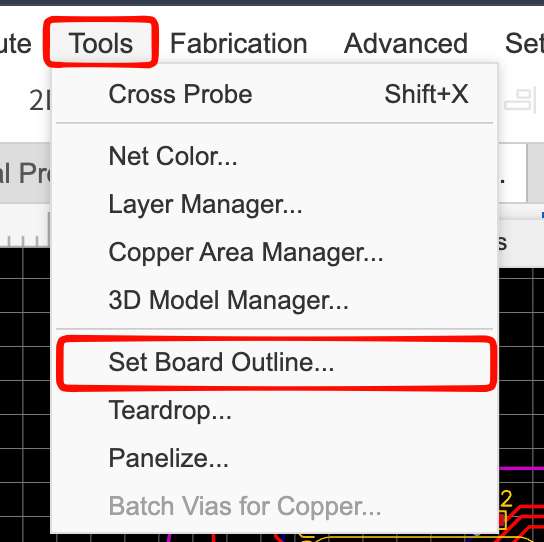
 You can adjust the border by clicking and dragging the vector points of the outline :
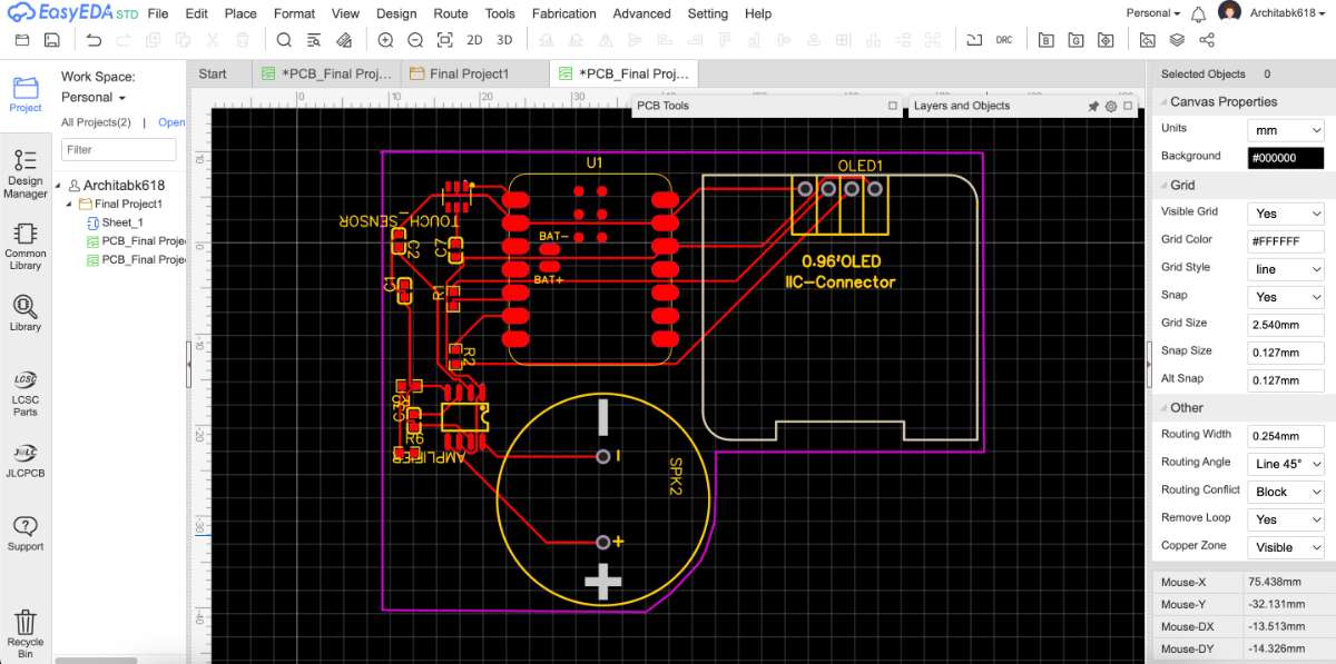 To View in 3d model,go to top toolbar, View → 3D view
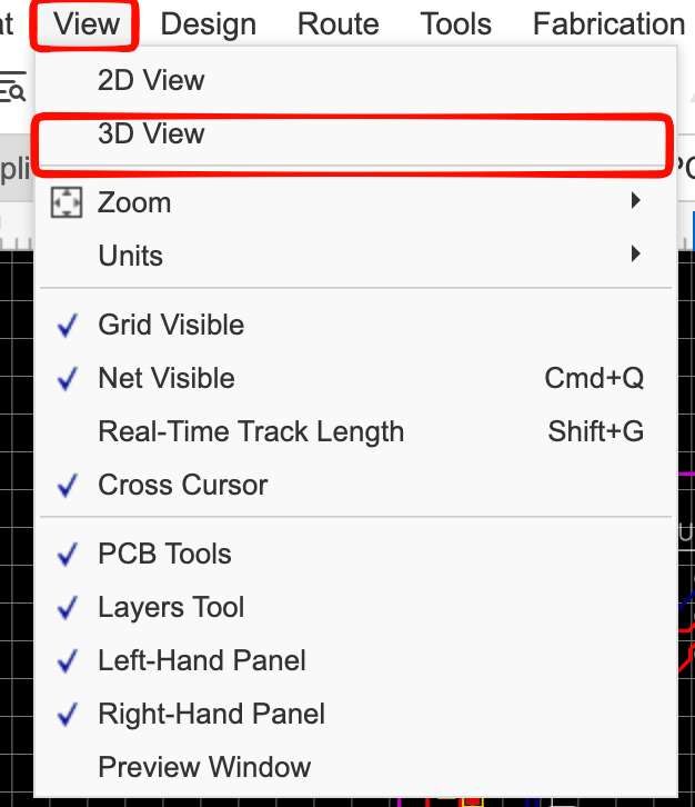 Here is the final Output :
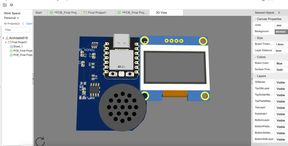
Conclusion
This week I learnt the basics of electronic CAD, using the lab's test equipment and working through a full PCB design from schematic to Gerbers.
Comparing the workflows I tried: designing for the XIAO felt the most natural to me because the board breaks out clean, well-labelled pins, so the schematic stayed simple. The ATtiny412 was a good first board to learn on — fewer pins, less to route but it made me think harder about which pins did what.
On the tools, KiCad is the one I'd reach for again: it's free, the Fab library plugs straight in, and the ERC/DRC checks caught my mistakes before fabrication. It has a bit of a learning curve at first. EasyEDA was the easiest to start with since it runs in the browser and has a huge built-in part library, and its auto-route saved time but I felt less in control of where things went. SnapEDA inside Fusion 360 was handy for grabbing parts and 3D models, though it gave me trouble on macOS and took time to appear in the toolbar. Overall, for full control and fabrication-ready output I prefer KiCad, while EasyEDA is my pick when I want to sketch something quickly.
Final Files
FUSION FILESEasyEDA Files
KiCAD FILES
WOKWI FILES