Week 6: Electronics Design
This week focuses on learning the fundamentals of electronic components, circuit principles, and PCB design workflows. I will study how components such as resistors, capacitors, diodes, transistors, connectors, and microcontrollers function within circuits, and review key electrical concepts like voltage, current, and power. I will also learn to use Electronic Design Automation (EDA) tools to create schematics, simulate circuits, and prepare PCB layouts while following proper design rules for fabrication.
Group assignment: Use the test equipment in our lab to observe the operation of an embedded microcontroller.
Individual assignment: Simulate a circuit and use an EDA tool to design an embedded microcontroller system using components from the lab inventory, and check the design rules for fabrication. (Extra credit: try another design workflow and/or design a case.)
Group Assignment Reflection
This Group assignment introduced a range of tools used for testing and debugging electronics.
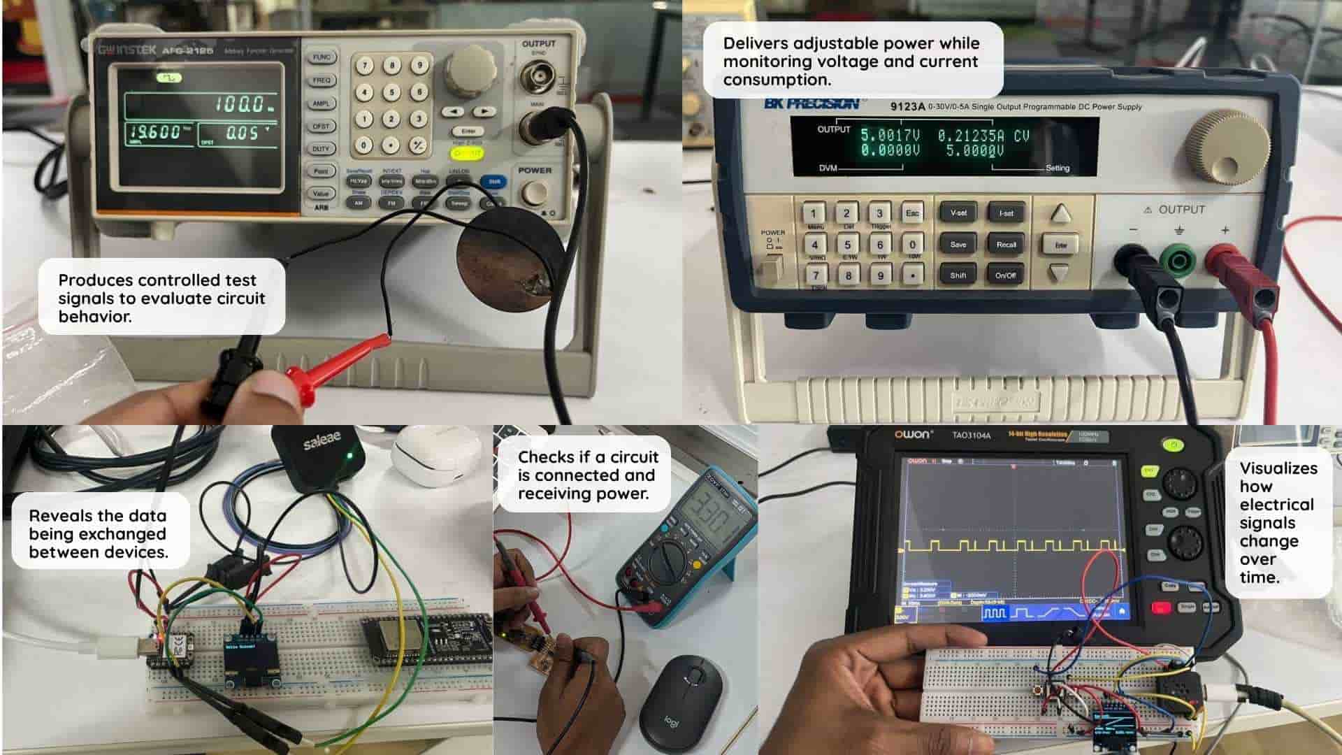
While the multimeter helped verify power, continuity, and component values, the oscilloscope made it possible to see how signals change over time. The logic analyzer provided a way to observe and decode communication between devices, and the function generator showed how different waveforms can be used to test electronic systems. The bench power supply highlighted the importance of supplying controlled power and setting safe current limits.
Together, these experiments showed that different tools reveal different parts of the same system, and choosing the right one makes troubleshooting much easier.


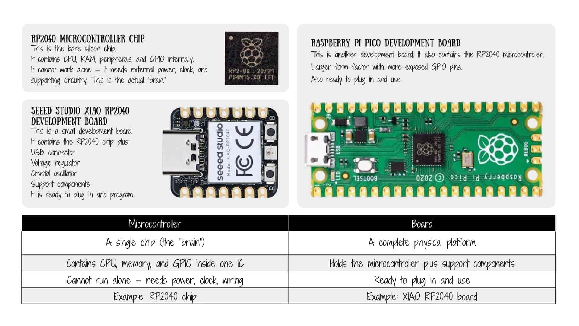
Understanding Microcontroller and Development Board
Simulation Introduction - Wokwi
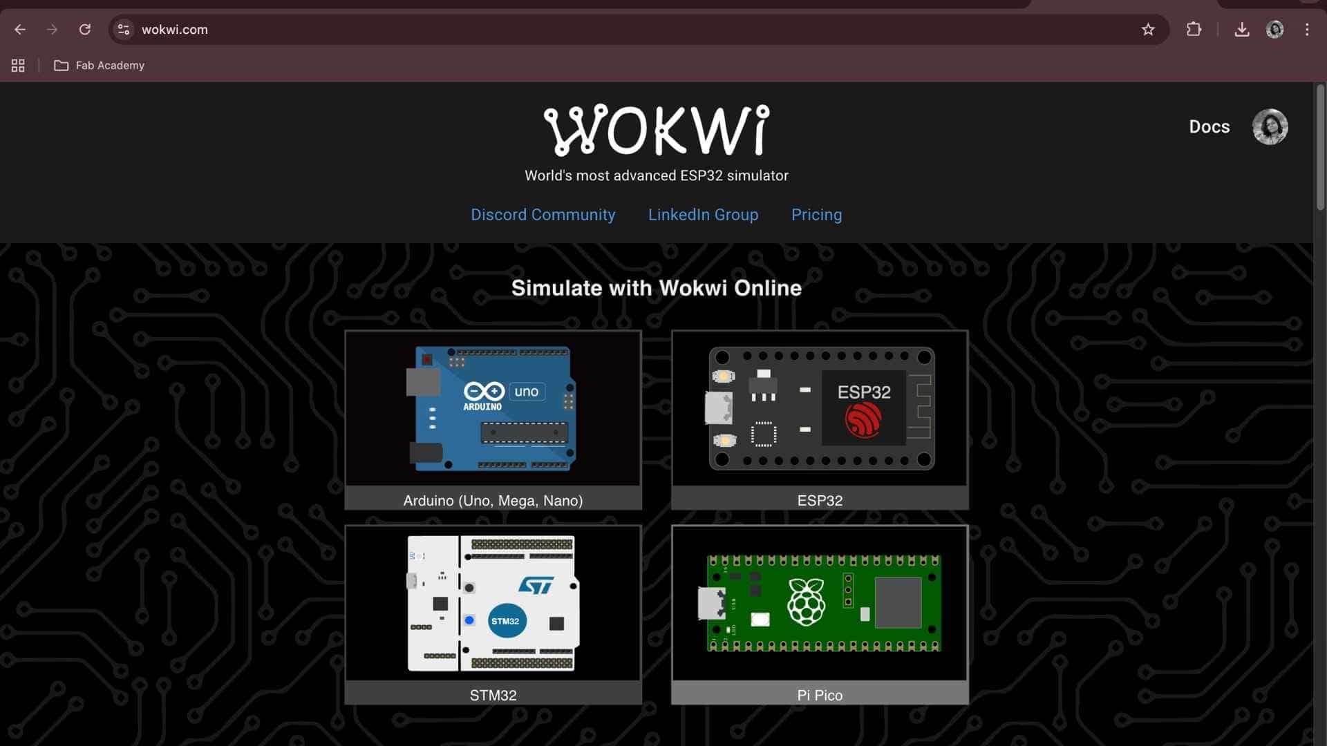
Once we were given a basic briefing on the foundational terms, we were introduced to a simulation tool called Wokwi. Wokwi is an online, browser-based electronics simulator that supports platforms such as Arduino, ESP32, Raspberry Pi Pico, and STM32. It allows users to design circuits, write code, and test embedded and IoT projects without physical hardware. It includes common components such as LEDs, sensors, and displays, and provides tools for testing and debugging through simulation.
Exploring Featured Example Projects
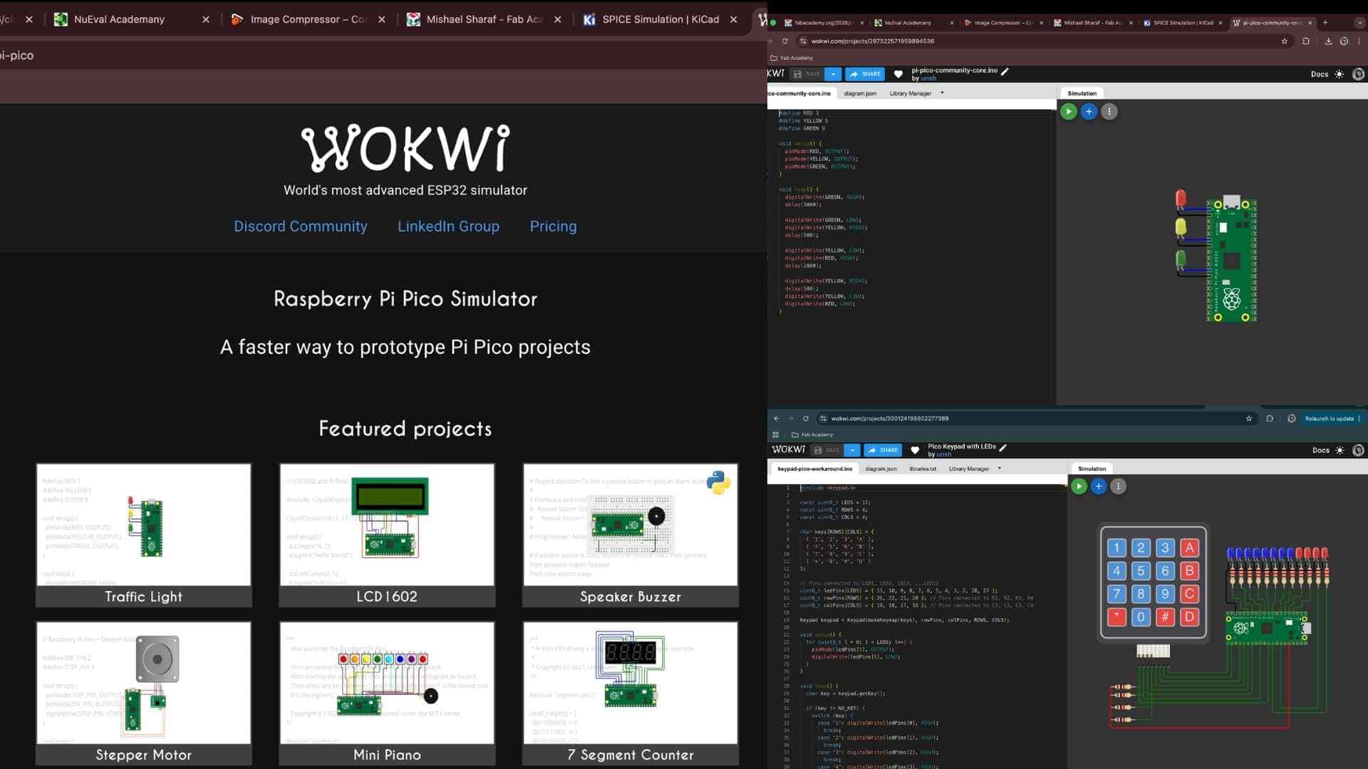
I began by signing into Wokwi and navigating to the Raspberry Pi Pico Simulator section. I explored featured example projects such as Traffic Light and Keypad and LEDs to understand how circuits and code interact within the simulation environment. The interface is divided into two main areas:
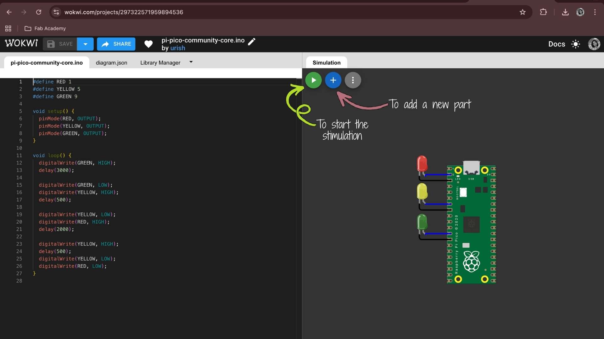
I experimented by modifying the delay values in the sample code and observed the changes directly in the simulation. This helped me understand how timing in code affects physical outputs such as LED blinking.
Recreating the Blink Program in Simulation
We were then asked to recreate the blink program that had previously been executed using the Arduino IDE. I copied my blink code from the Arduino IDE and pasted it into a new Wokwi project. I built a simple circuit consisting of:
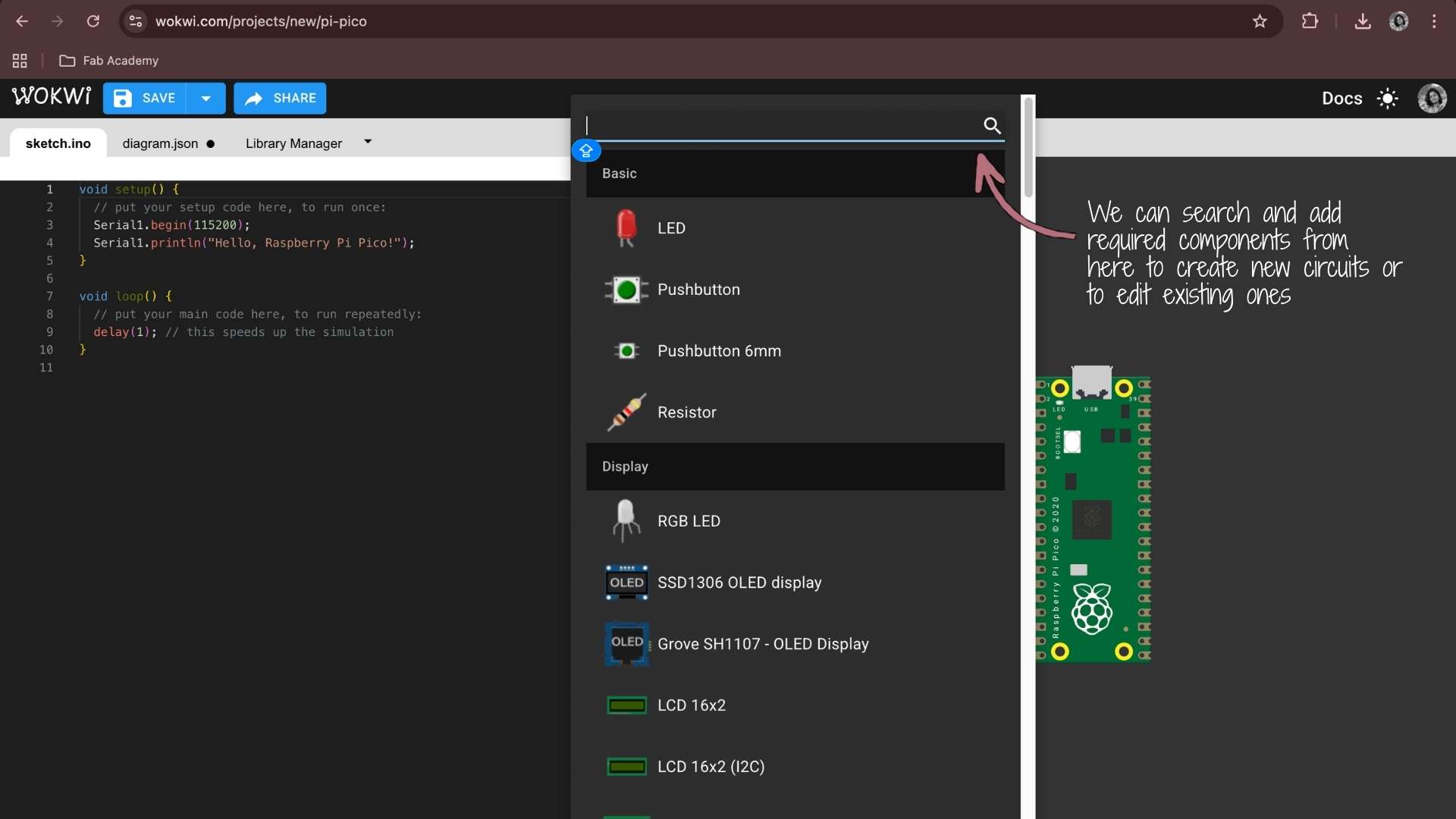
Circuit Connections
The circuit was connected as follows:
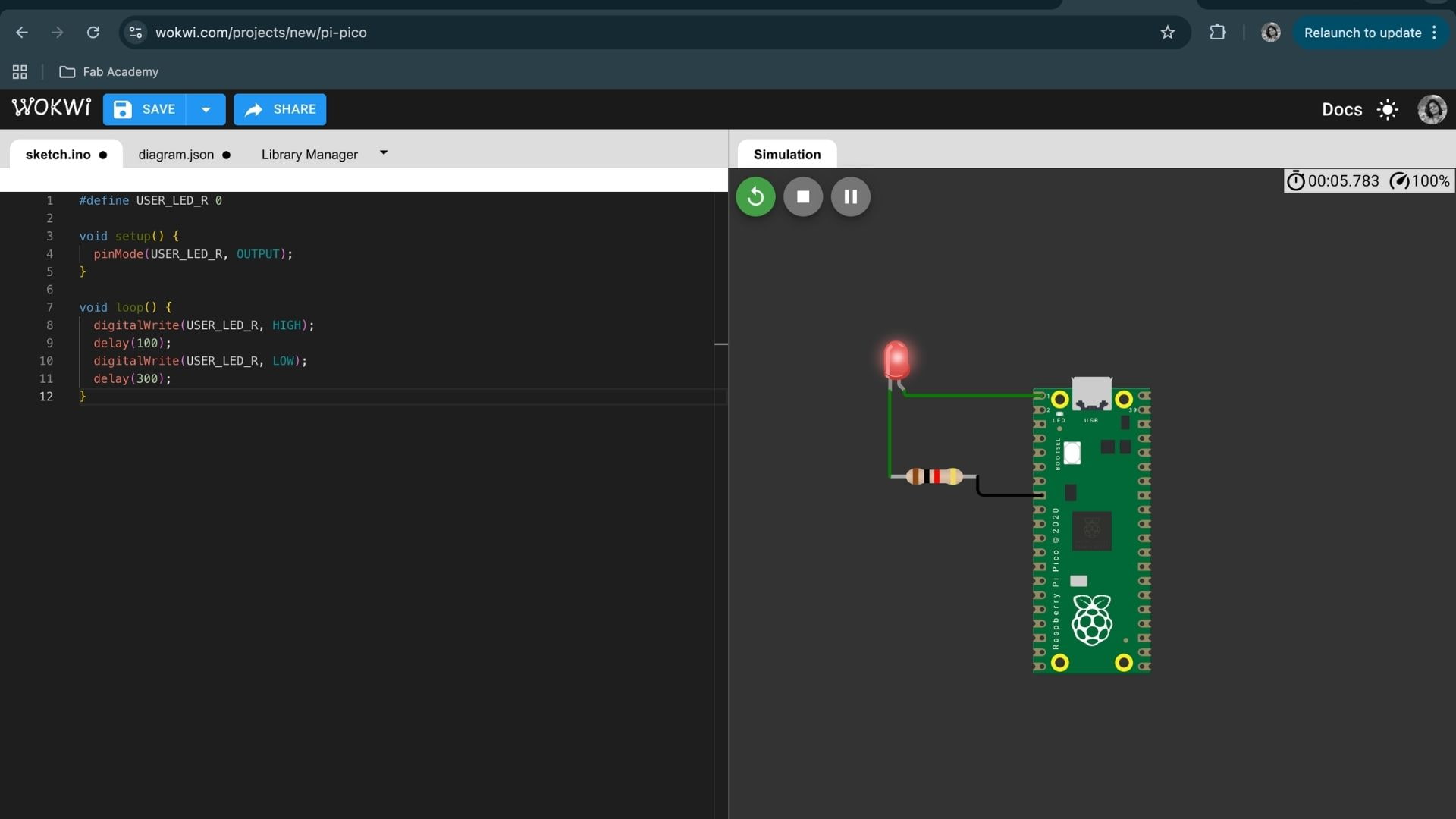
Blink Code Used:
#define USER_LED_R 0

void setup() {
  pinMode(USER_LED_R, OUTPUT);
}

void loop() {
  digitalWrite(USER_LED_R, HIGH);
  delay(100);
  digitalWrite(USER_LED_R, LOW);
  delay(300);
}
Simulation Result
After completing the circuit and uploading the code, I pressed the Play button to start the simulation. The LED blinked according to the programmed delay values, confirming that the circuit and code were functioning correctly.
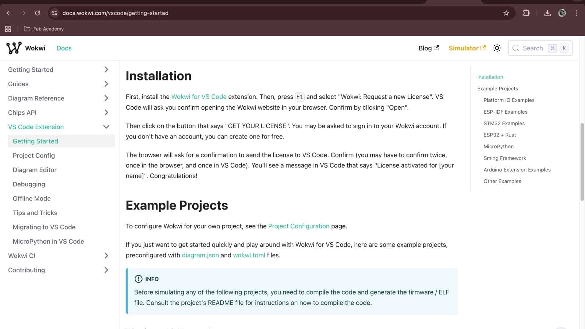
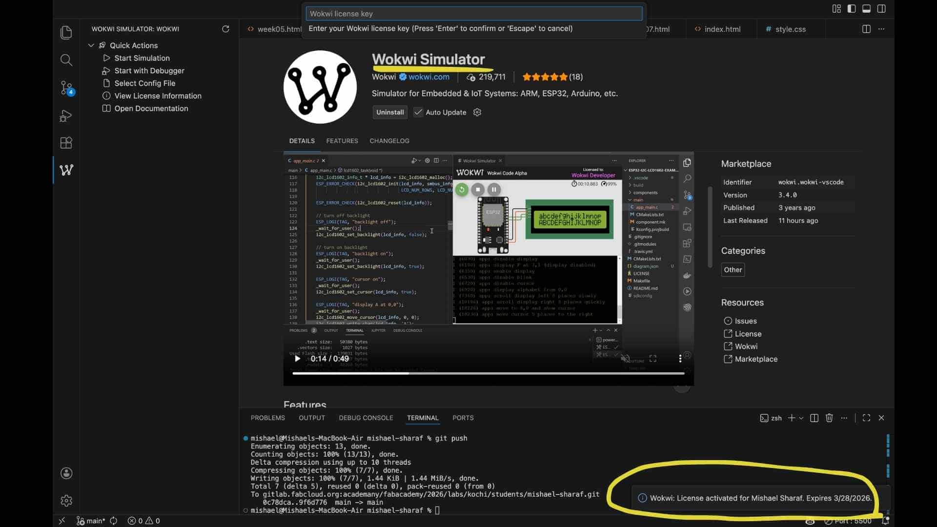
Installing the Wokwi Extension for VS Code
After using Wokwi in the browser, we proceeded to install the Wokwi extension for Visual Studio Code (VS Code) by following the official setup guide.
The installation process involved:
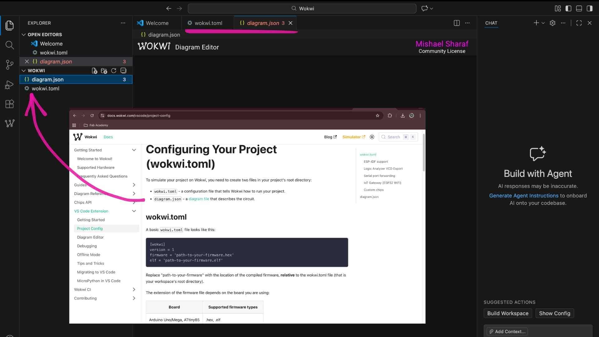
Configuring Projects in VS Code
After installing and activating the Wokwi extension in VS Code, the simulator required project configuration files to run correctly. According to the documentation, two files must be present in the project root folder:
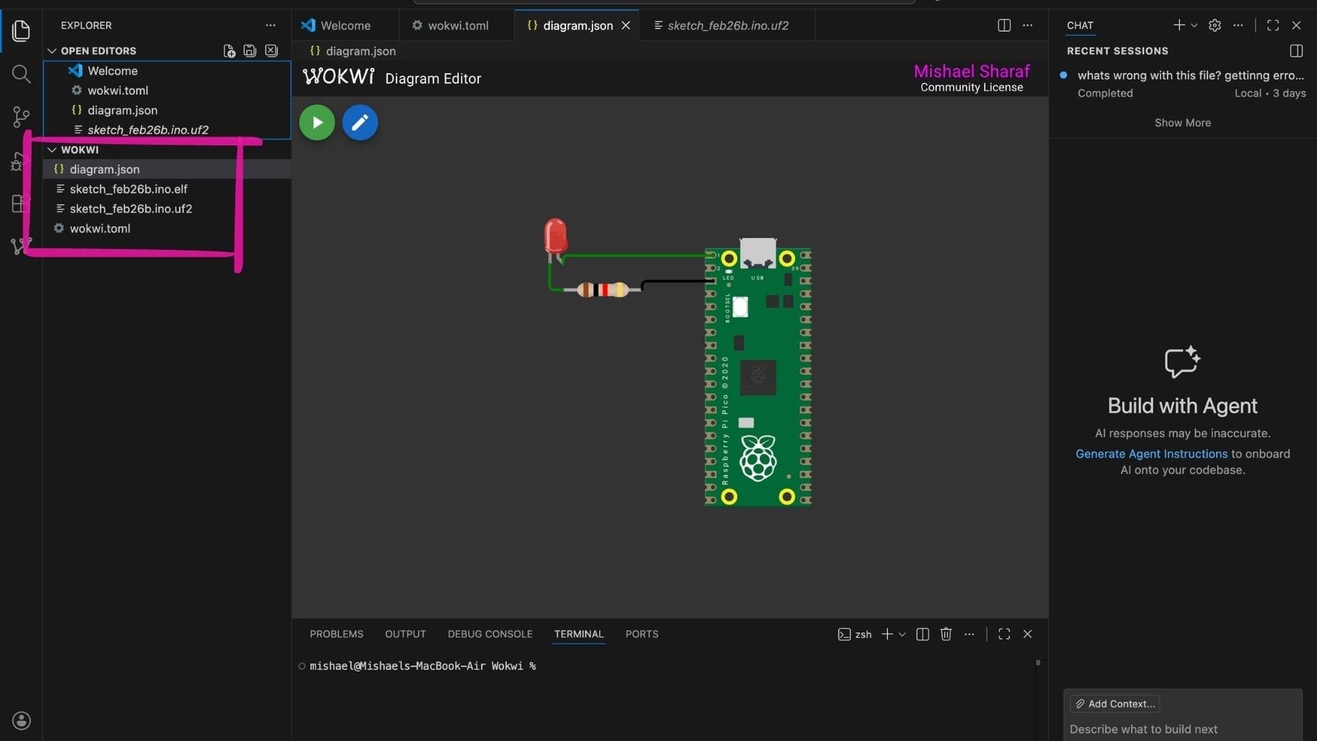
Adding Firmware Files from Arduino IDE
Since I had already created and tested a blink program using the Arduino IDE, I used the compiled firmware from that project. The Raspberry Pi Pico uses compiled firmware files such as:
Chase LED with Button Control | Wokwi Simulation Documentation
Objective: Create a four-LED chase sequence that runs only when a push button is pressed. When the button is not pressed, all LEDs remain off. This demonstrates:
Hardware Components
Wokwi Work Interface
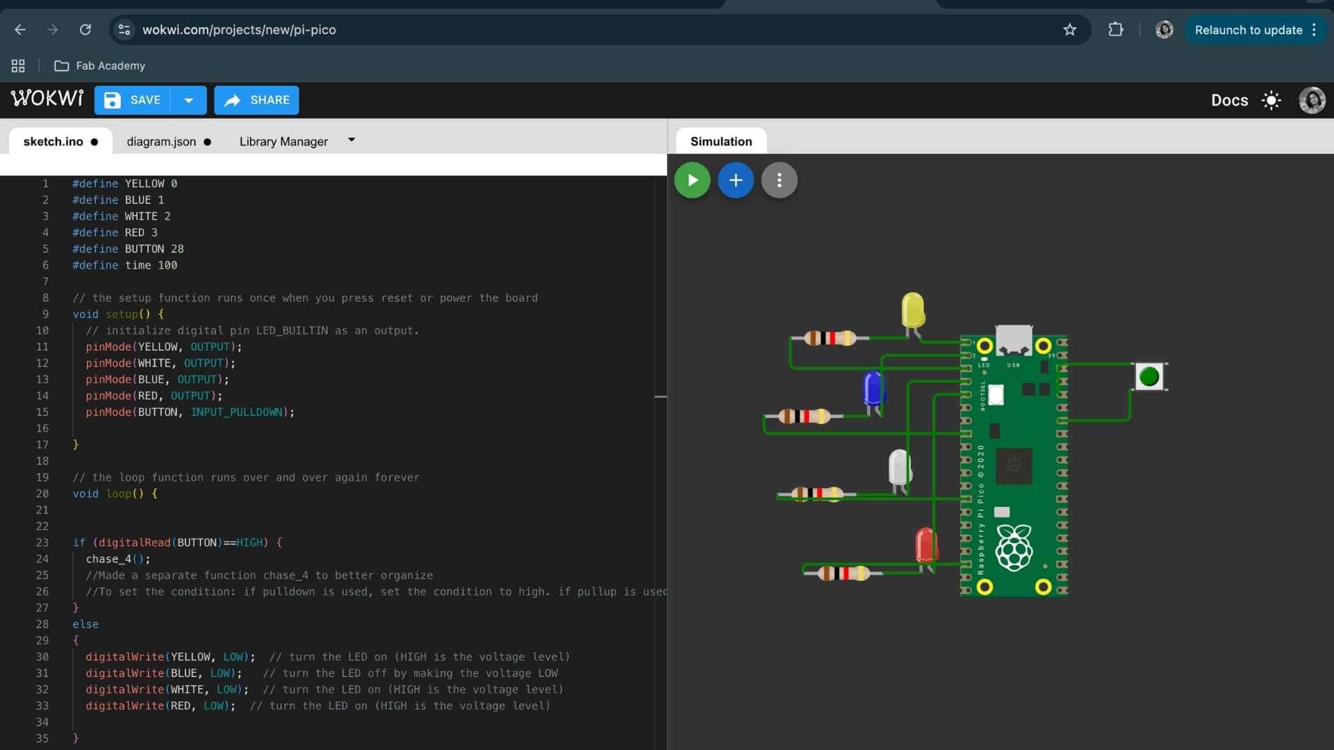
Code:
#define YELLOW 0
#define BLUE 1
#define WHITE 2
#define RED 3
#define BUTTON 28
#define time 100

// the setup function runs once when you press reset or power the board
void setup() {
  // initialize digital pin LED_BUILTIN as an output.
  pinMode(YELLOW, OUTPUT);
  pinMode(WHITE, OUTPUT);
  pinMode(BLUE, OUTPUT);
  pinMode(RED, OUTPUT);
  pinMode(BUTTON, INPUT_PULLDOWN);

}

// the loop function runs over and over again forever
void loop() {


if (digitalRead(BUTTON)==HIGH) {
  chase_4();
  //Made a separate function chase_4 to better organize
  //To set the condition: if pulldown is used, set the condition to high. if pullup is used, set it to low
}
else
{
  digitalWrite(YELLOW, LOW);  // turn the LED on (HIGH is the voltage level)
  digitalWrite(BLUE, LOW);   // turn the LED off by making the voltage LOW
  digitalWrite(WHITE, LOW);  // turn the LED on (HIGH is the voltage level)
  digitalWrite(RED, LOW);  // turn the LED on (HIGH is the voltage level)

}

}

// to run the leds as a ring
void chase_4()
{

  digitalWrite(YELLOW, HIGH);
  digitalWrite(BLUE, LOW);
  digitalWrite(WHITE, LOW);
  digitalWrite(RED, LOW);
  delay(time);

  digitalWrite(YELLOW, LOW);
  digitalWrite(BLUE, HIGH);
  digitalWrite(WHITE, LOW);
  digitalWrite(RED, LOW);
  delay(time);


  digitalWrite(BLUE, LOW);
  digitalWrite(WHITE, HIGH);
  digitalWrite(YELLOW, LOW);
  digitalWrite(RED, LOW);
  delay(time);

  digitalWrite(WHITE, LOW);
  digitalWrite(RED, HIGH);
  digitalWrite(BLUE, LOW);
  digitalWrite(YELLOW, LOW);
  delay(time);
}
Installing KiCad
I first installed KiCad on macOS. KiCad is a free and open-source Electronic Design Automation (EDA) software suite used for creating schematic diagrams and designing printed circuit boards (PCBs). It provides a complete professional workflow without licensing restrictions, making it suitable for both learning and production-level PCB design.
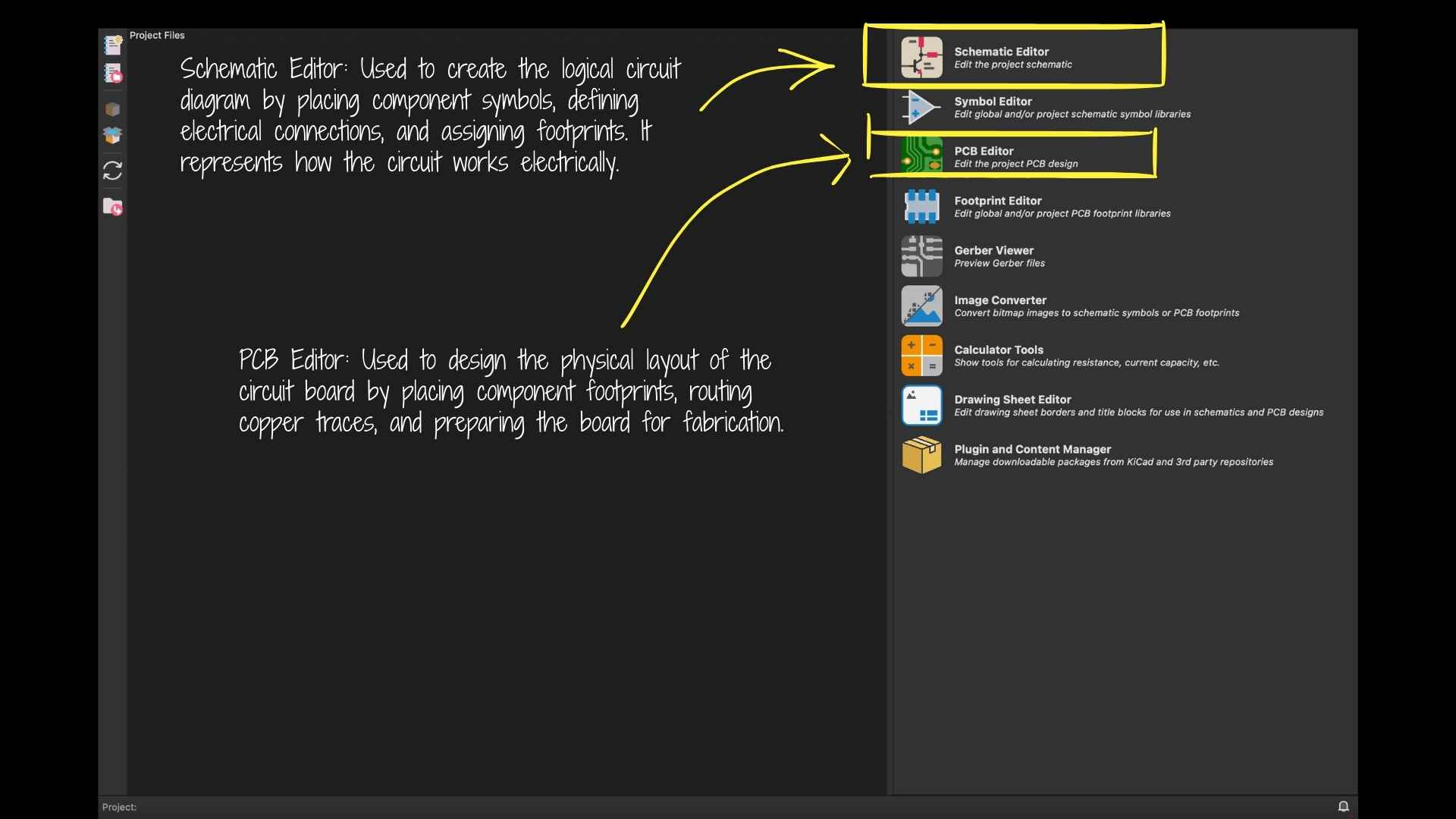
Understanding the KiCad Workflow
We were introduced to KiCad’s main workflow through its different editors:
These tools together allow the transition from conceptual circuit design to manufacturable PCB files.
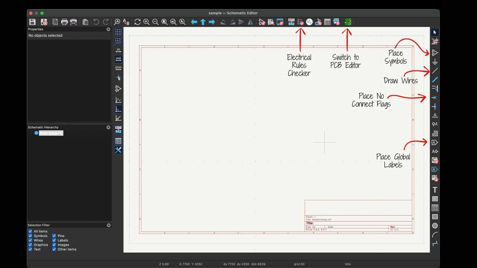
Creating the Circuit in the Schematic Editor
For the class exercise, we began by opening the Schematic Editor, which provides access to the symbol libraries used to place electronic components.
We installed the Fab Academy KiCad library from: KiCAD Library.
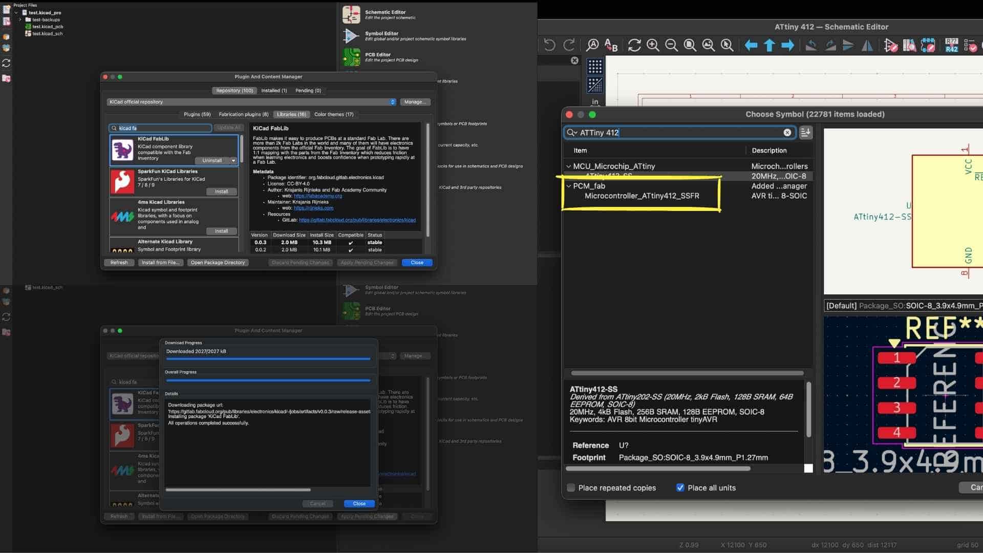
After installing and configuring the library, components from this collection appeared with the prefix “fab” in the search results. These libraries contain footprints and symbols specifically prepared for digital fabrication workflows.
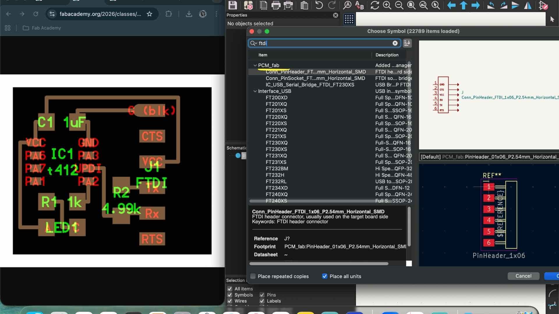
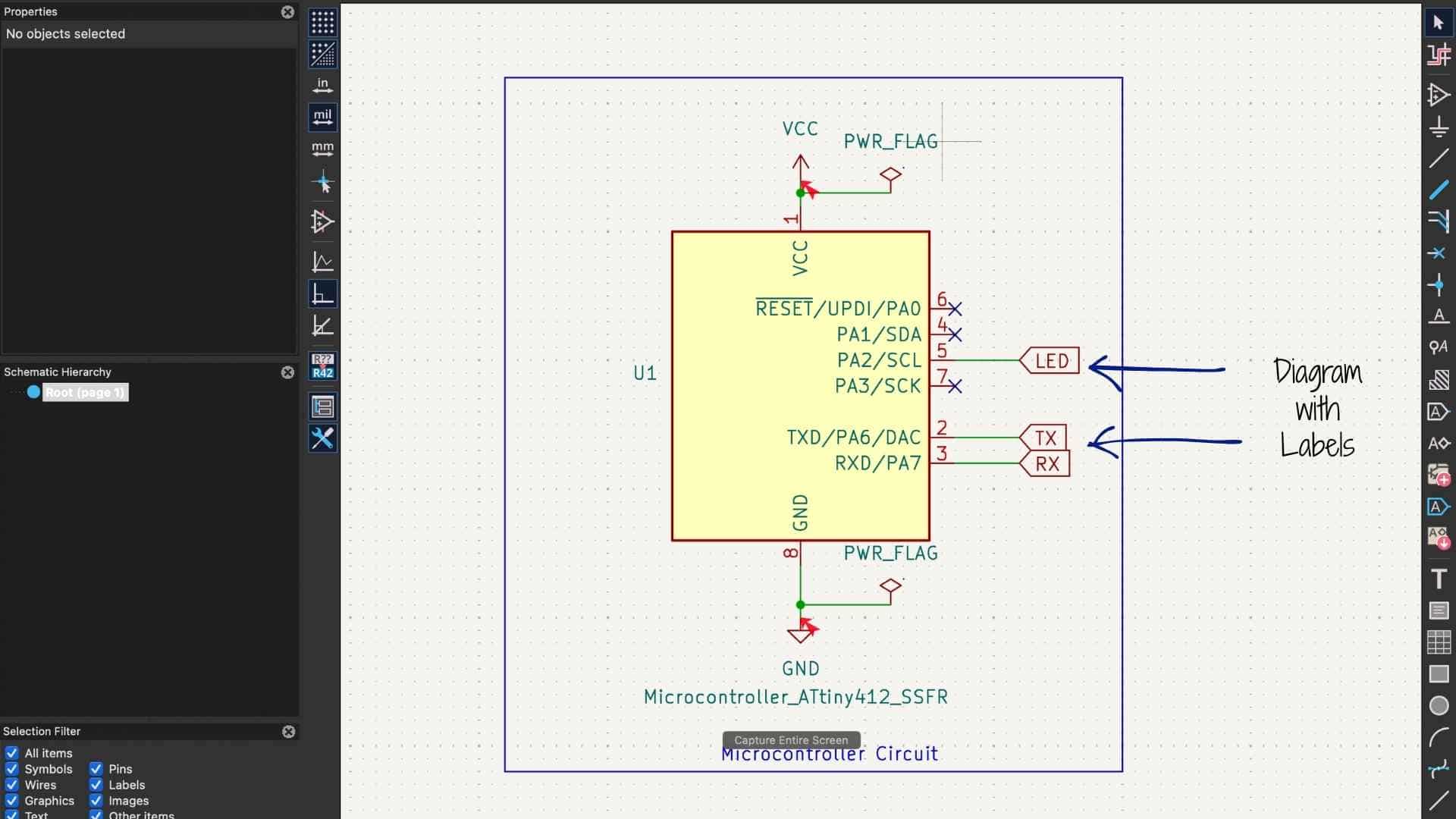
Recreating and Modifying the ATtiny412 Circuit
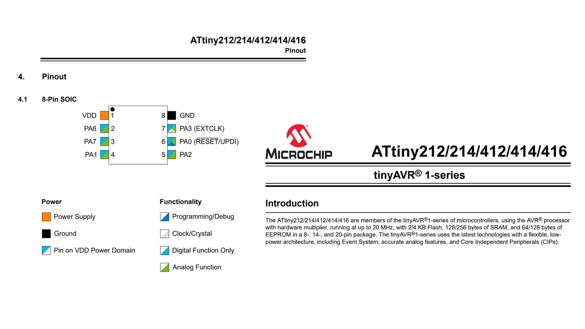
As a reference, we used Neil's ATtiny412 blink board from the embedded programming week. Following the reference diagram, we recreated the circuit using components from the Fab library. During this process, we:
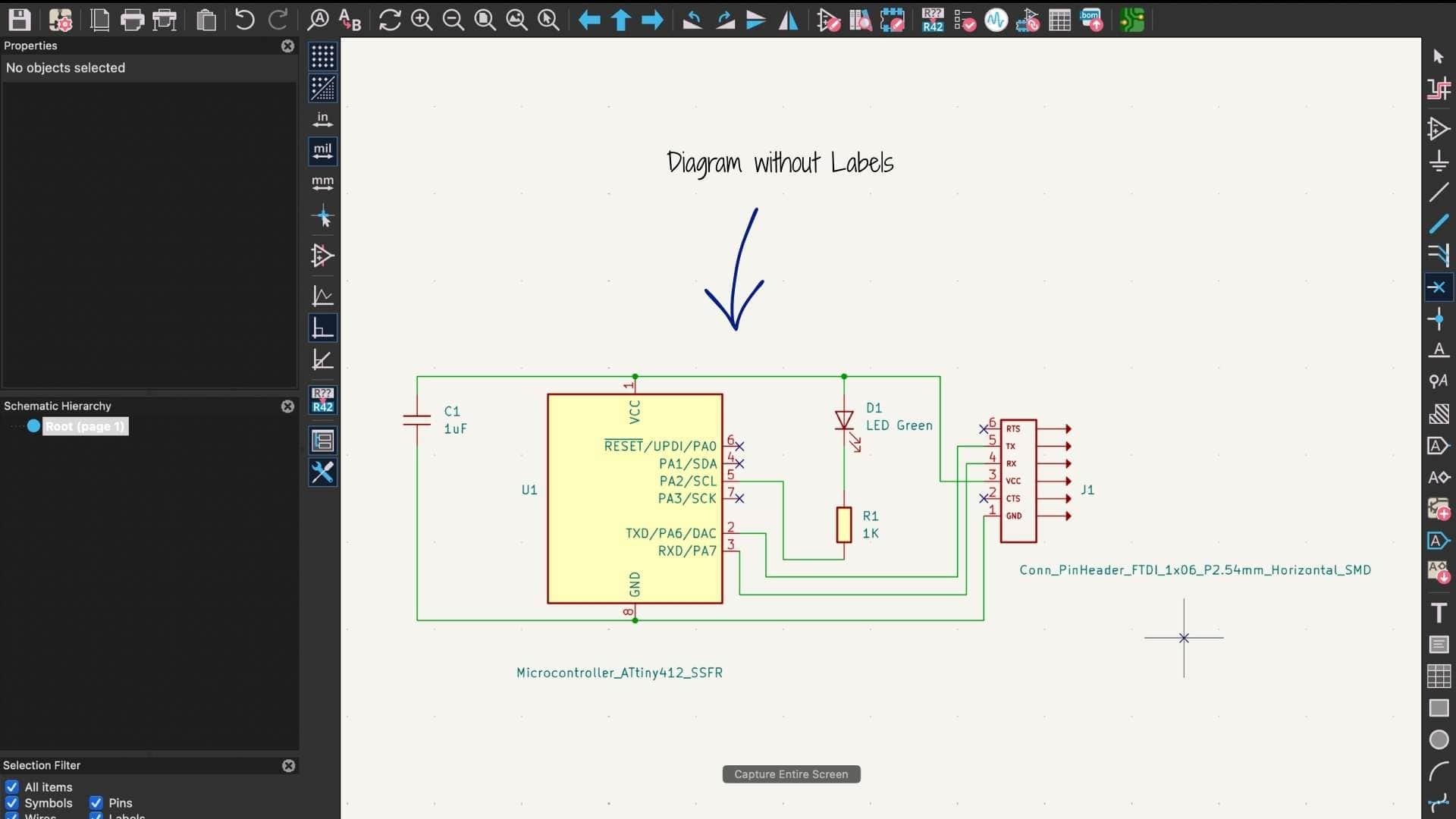
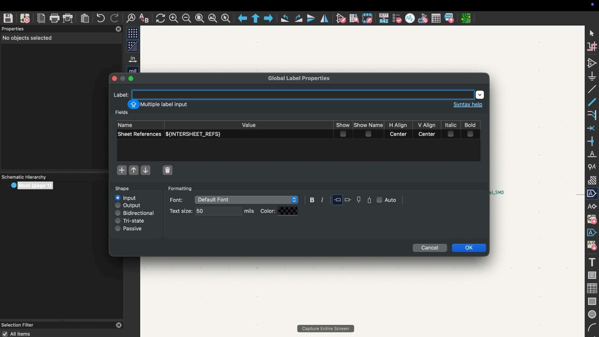
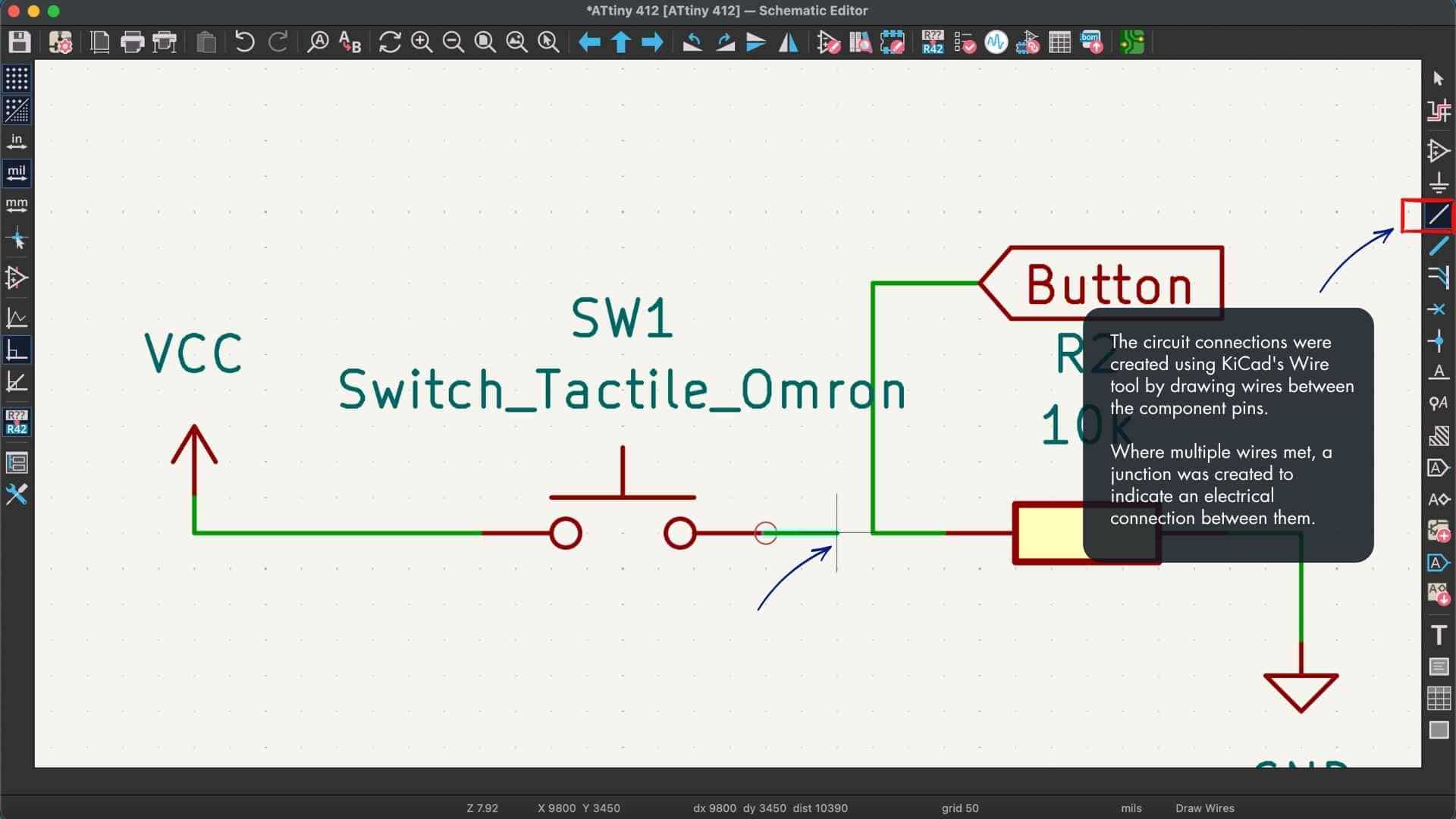
Using Global Labels for Clean Connections
To avoid excessive wire crossings and improve readability, we used the Place Global Label tool. Labels allow connections between components without drawing long physical wires, making the schematic cleaner and easier to understand.
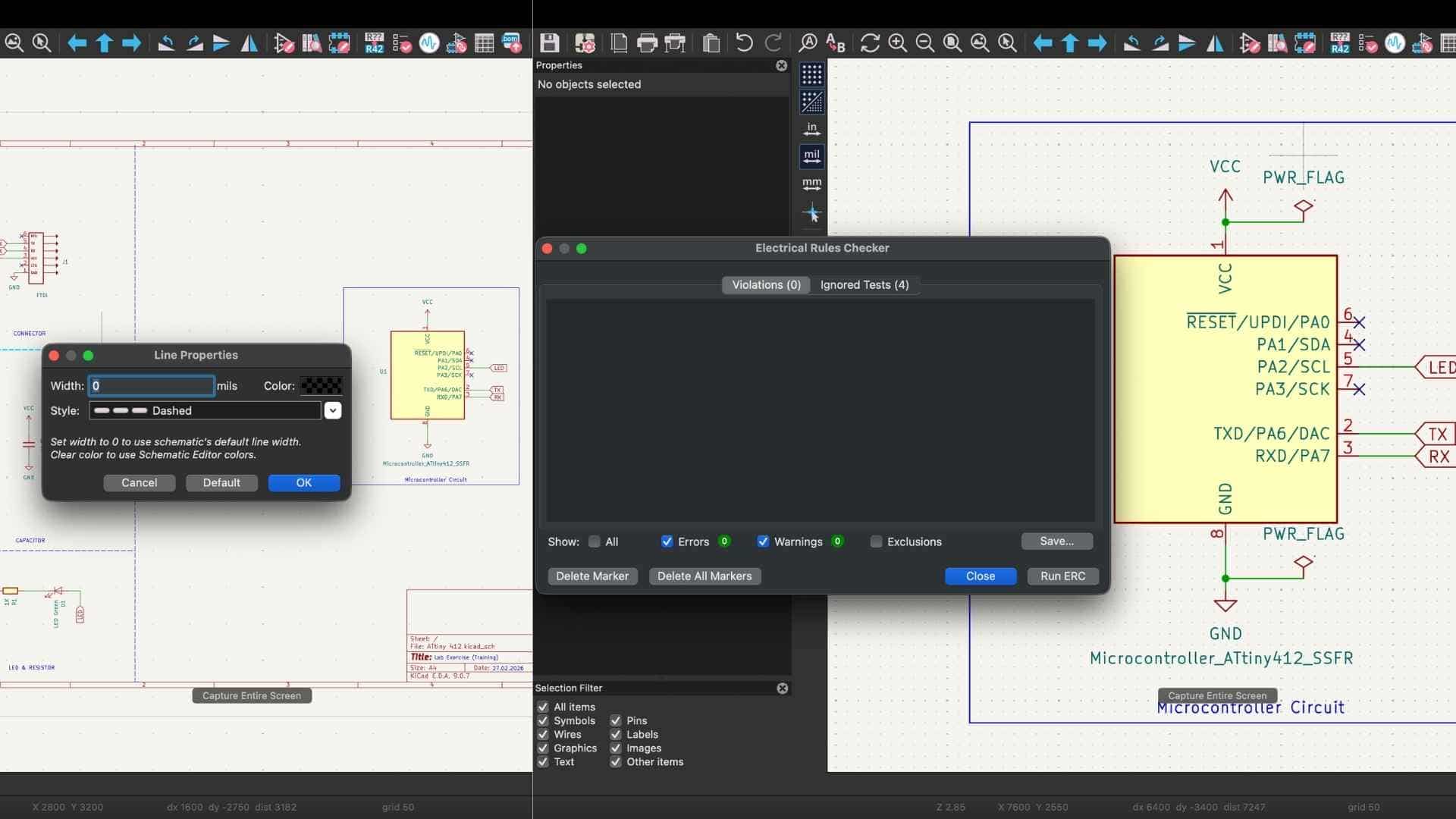
Electronical Rules Checker (ERC)
Transferring the Design to the PCB Editor
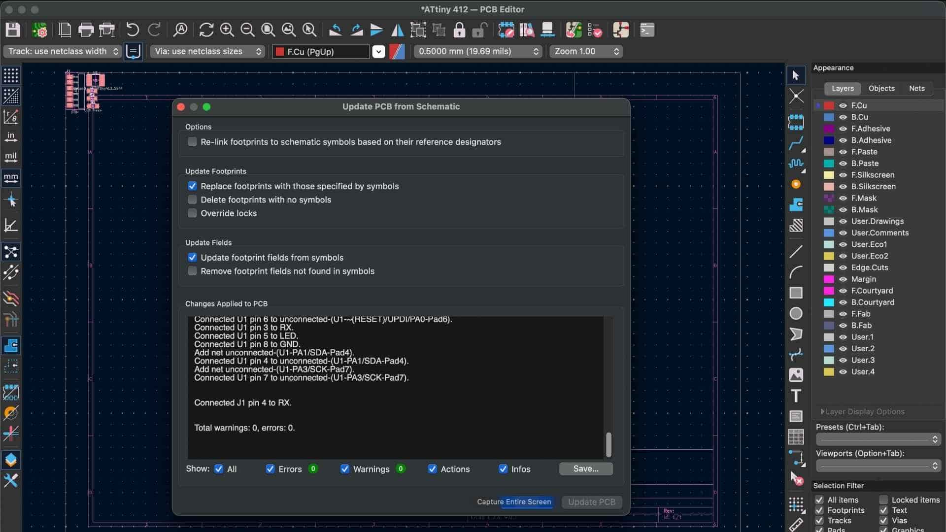
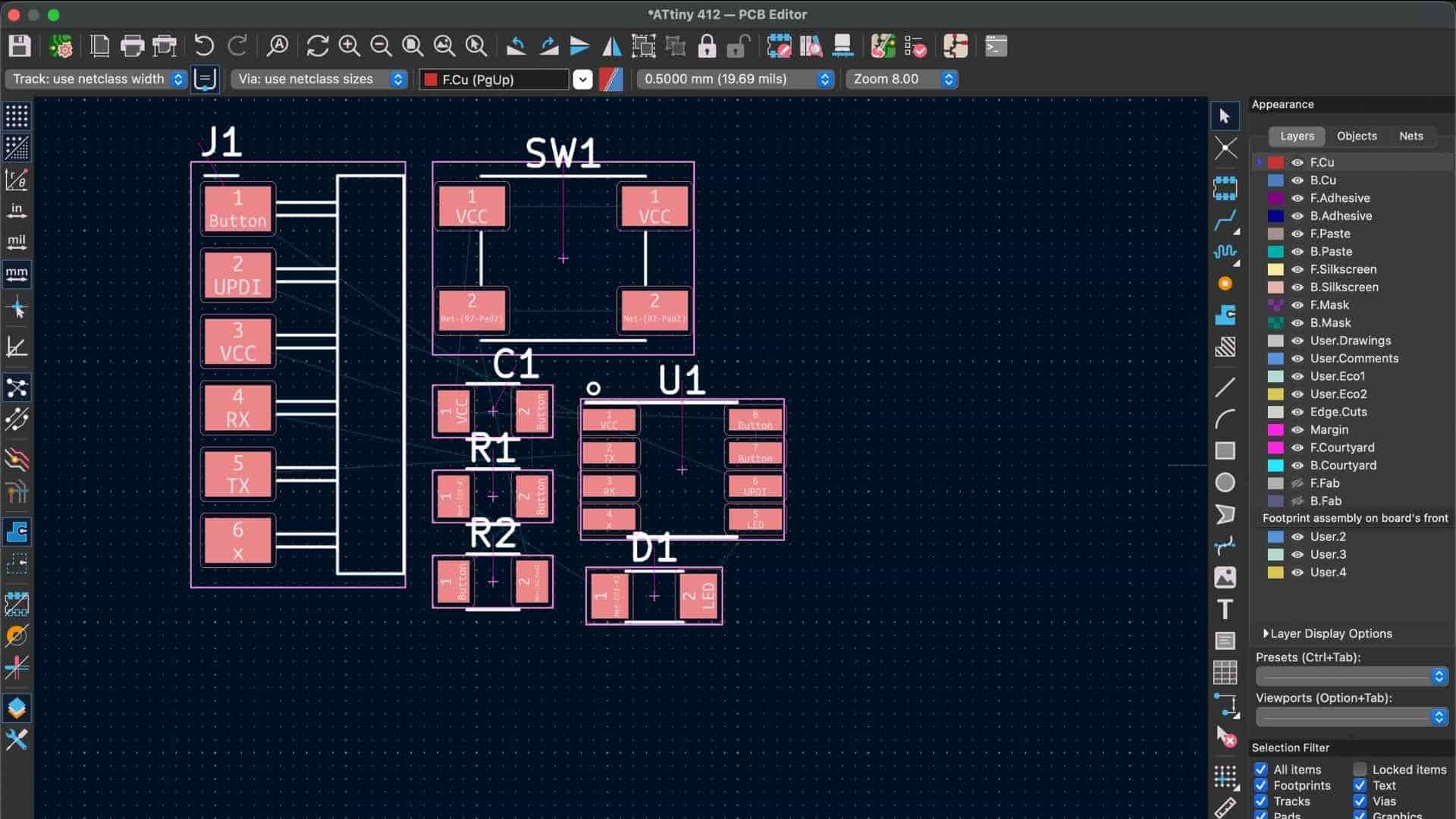
Once the schematic was complete, we opened the PCB Editor and imported the schematic into the layout environment. This generated the updated schematic and placed all components. In the PCB Editor, we performed the following tasks:
This stage defines the physical structure of the PCB.
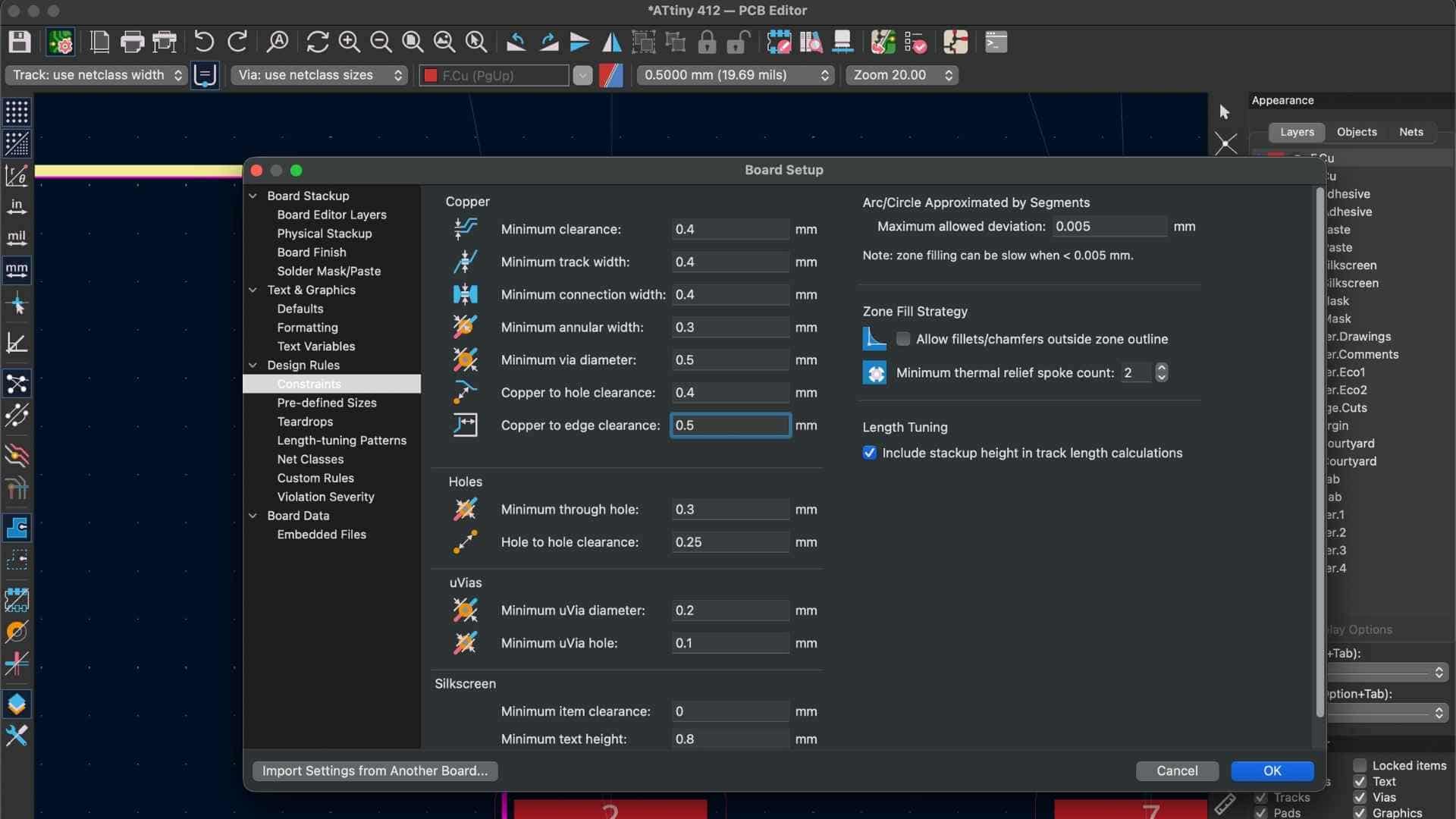
Configuring Design Rules
Before routing the PCB, I configured the design rules in KiCad to match the manufacturing constraints of the milling process. The values for minimum track width, clearance, and other parameters were based on the recommendations provided by our instructor. Setting these limits early helps prevent routing errors and ensures that the board can be manufactured reliably.
Running Design Rule Checks and Viewing in 3D
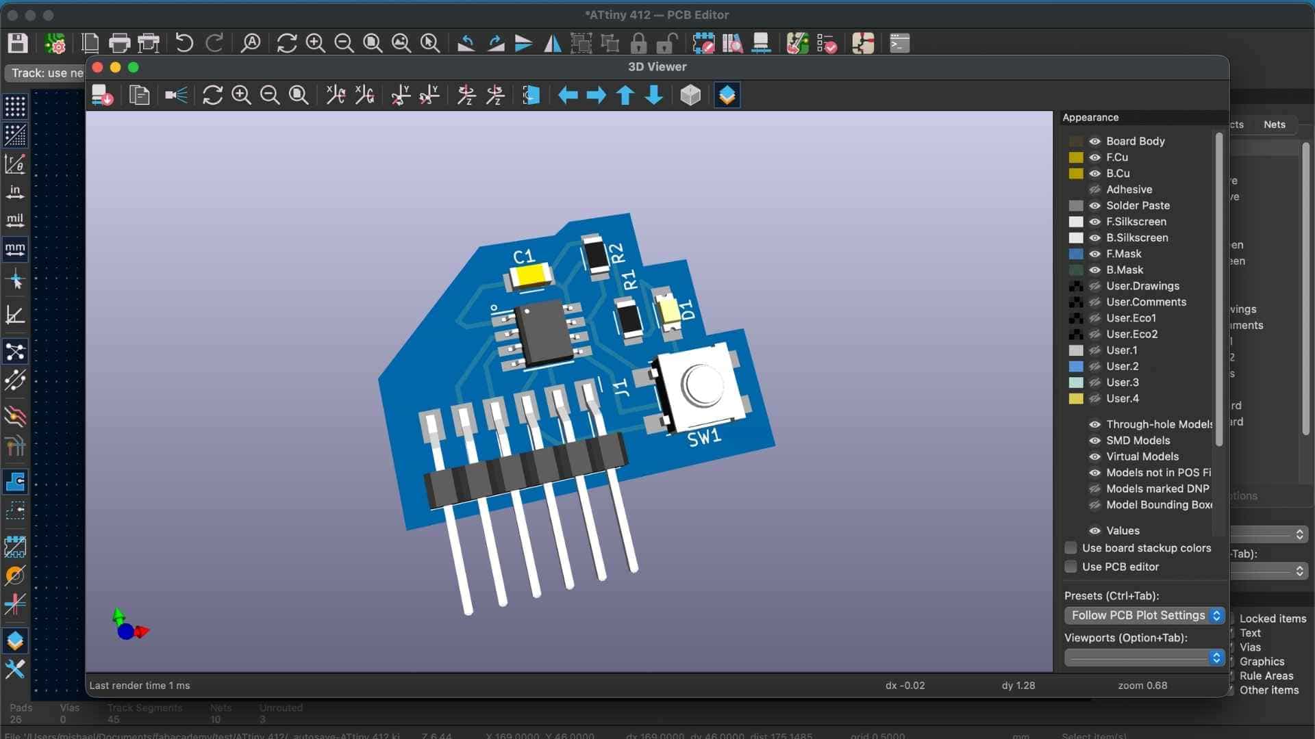
Before finalizing the design, we ran the Design Rules Checker (DRC) to ensure there were no electrical or manufacturing errors. After resolving all issues and achieving zero errors, we used the 3D Viewer to inspect the final board visually. This step helps confirm the physical feasibility of the design.
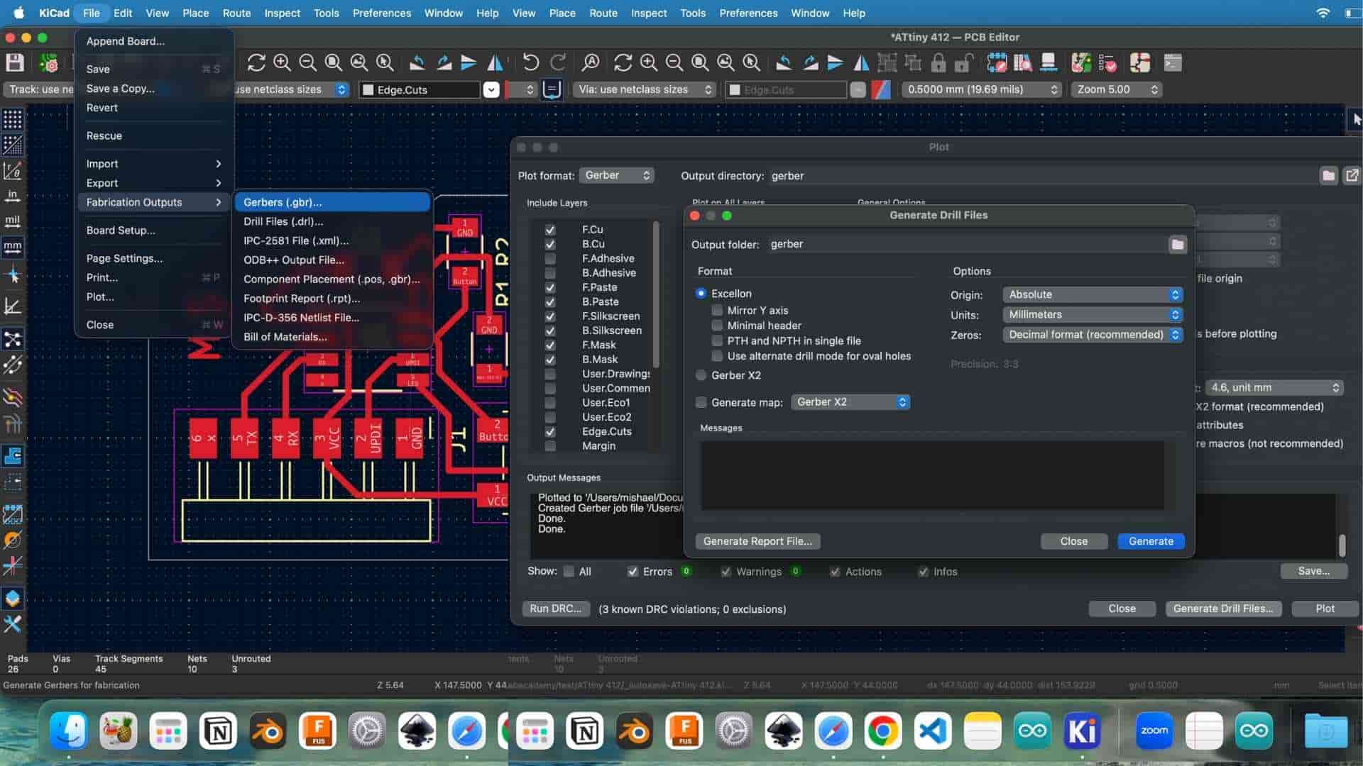
Generating Gerber Files for Fabrication
To prepare the design for manufacturing, we exported the files by navigating to: File → Fabrication Outputs → Gerber Files Gerber files (.gbr) are the standard format used in PCB fabrication. They define all layers of the board, including:
These files act as the blueprint used by PCB milling machines or fabrication services.
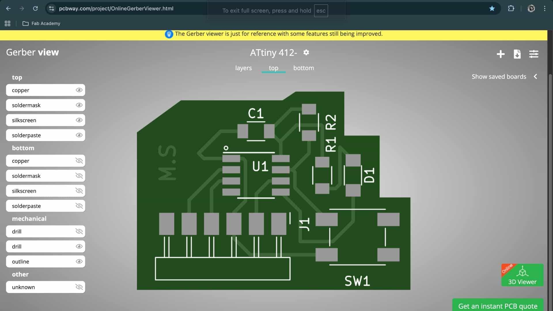
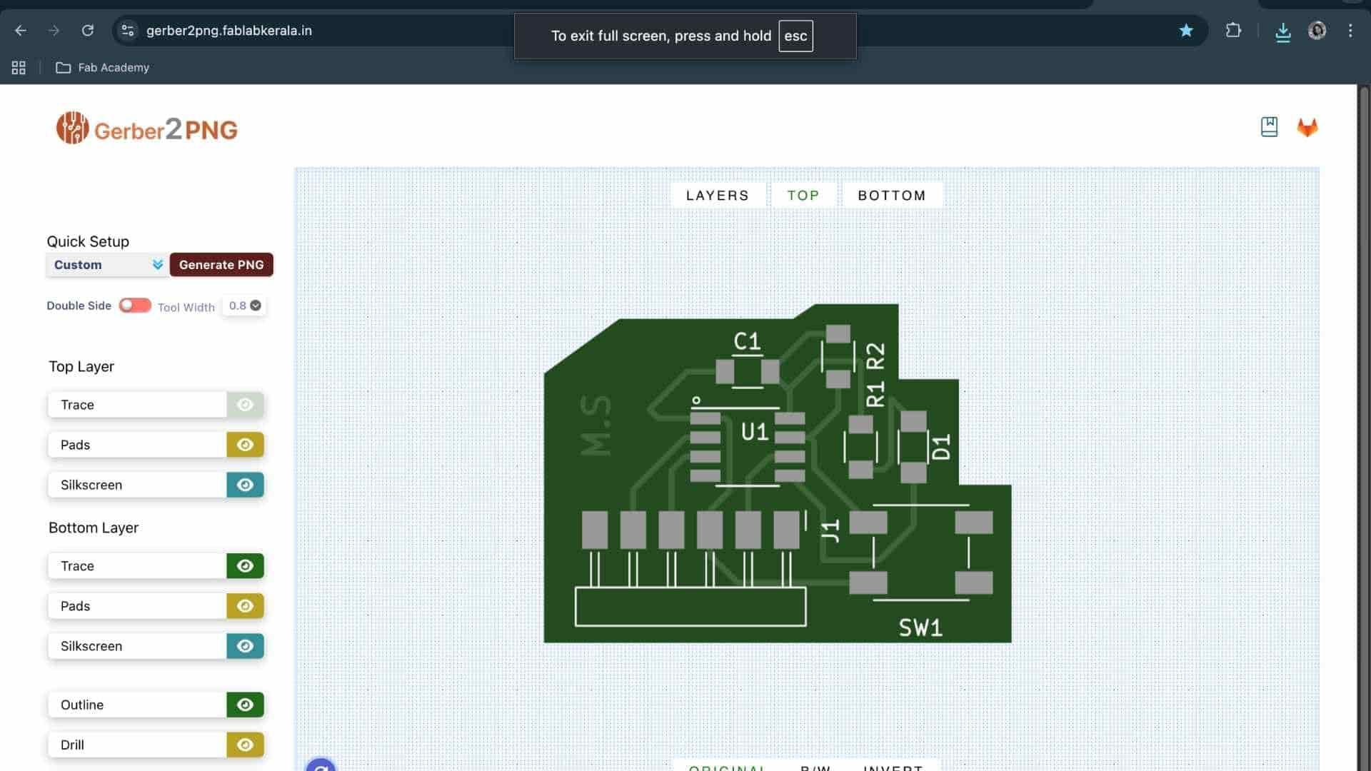
Viewing the Gerber Files
To verify the exported files, we used the online Gerber viewer: pcbway and gerber2png This allowed us to visualize each PCB layer and confirm that the traces, pads, and board outline were correct before fabrication.
The ATtiny412 board was used as a training exercise to become familiar with the KiCad workflow before working on my own PCB design.
Custom PCB Design - Individual Assignment
For this assignment, I designed a custom PCB using the Seeed Studio XIAO RP2040 as the microcontroller. The overall workflow followed the same KiCad process used during the guided class exercise
(schematic → ERC → footprint assignment → PCB layout → DRC → 3D inspection).
Therefore, instead of repeating the entire workflow, this documentation focuses on board-specific decisions, references, and checks performed during the design process.
Pin Mapping and Reference Material
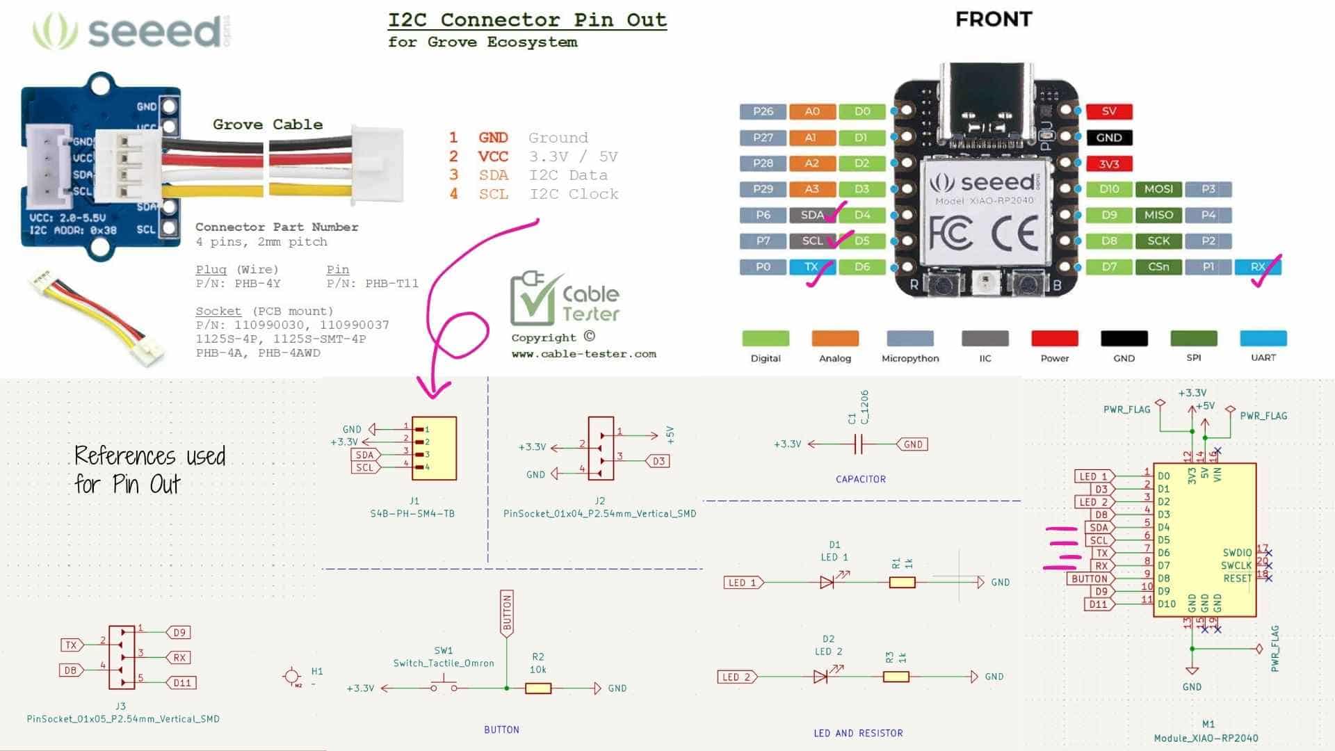
Before creating the schematic, I referred to the XIAO RP2040 pinout diagram and the Grove I2C connector pin configuration. The Grove I2C connector uses a 4-pin layout:
Using these references, I mapped the pins in the schematic as follows:
These references ensured that the connector layout and microcontroller pins matched the intended communication interfaces.
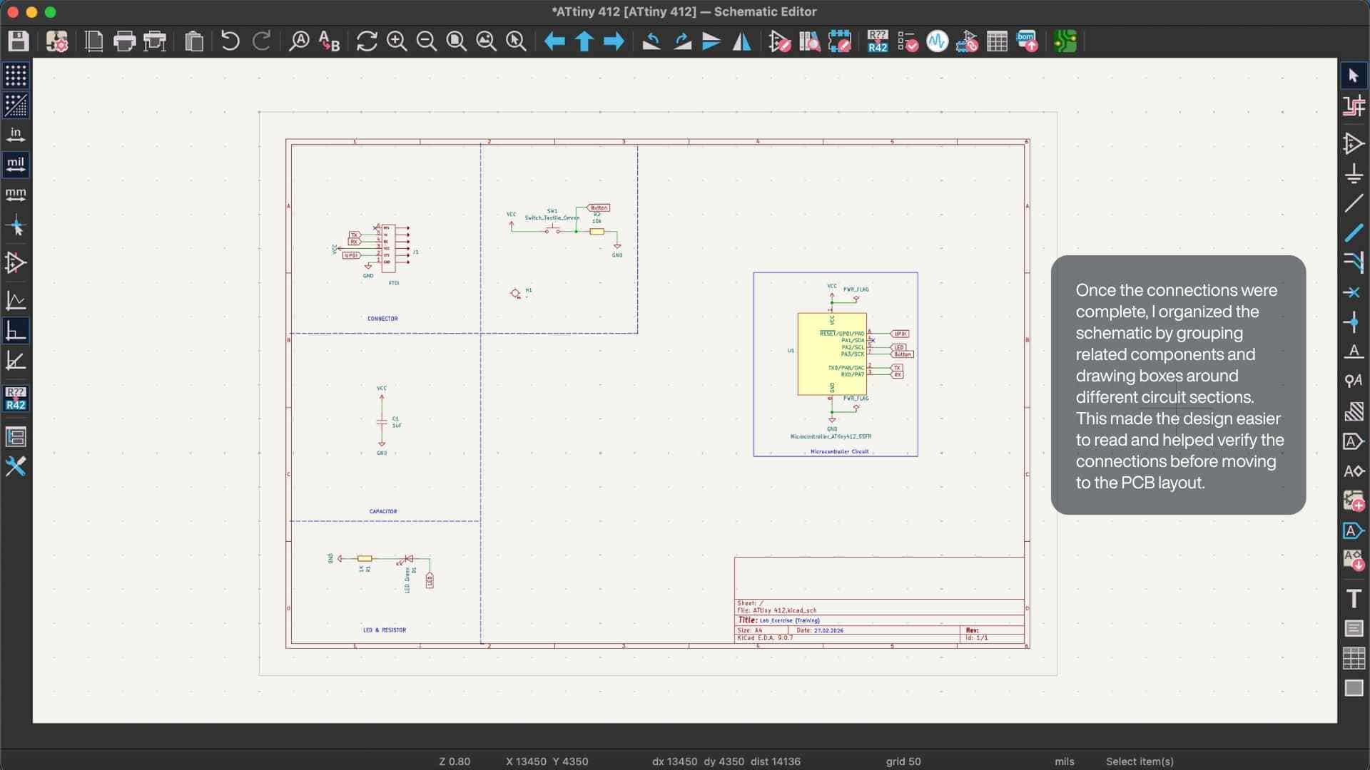
Schematic Organization
The schematic was organized into functional sections to make the design easier to read and debug:
Electrical Rules Check (ERC)
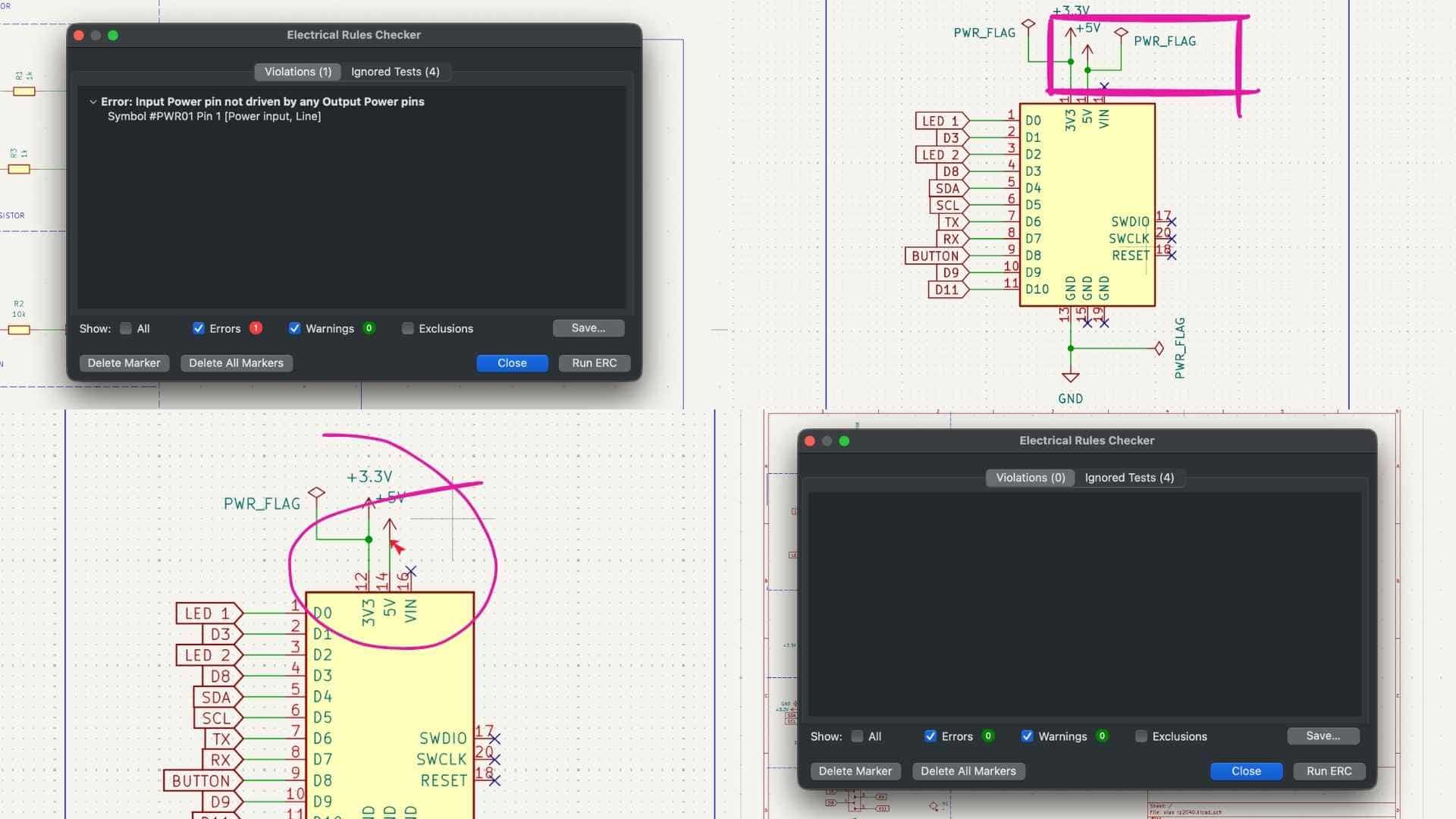
While running the Electrical Rules Checker (ERC), KiCad initially reported the error:
Input power pin not driven by any output power pins
This occurs when KiCad cannot identify the source of a power net.
To resolve this, I placed a PWR_FLAG on the power line. This tells KiCad that the net is intentionally powered. After adding the flag and re-running ERC, the error was resolved
Notes:
What's a UART Connector?
A UART connector exposes the serial communication interface of a microcontroller so that external devices can communicate with it.
UART stands for Universal Asynchronous Receiver–Transmitter. It is one of the simplest communication protocols used in embedded systems.
Core Signals
Typical UART connections include:Data is transmitted bit-by-bit over two lines (TX and RX), without a shared clock signal. In my board and schematic:
The connector labeled J3 exposes these pins so that the board can communicate with:
This connector essentially acts as a serial communication port for the PCB.
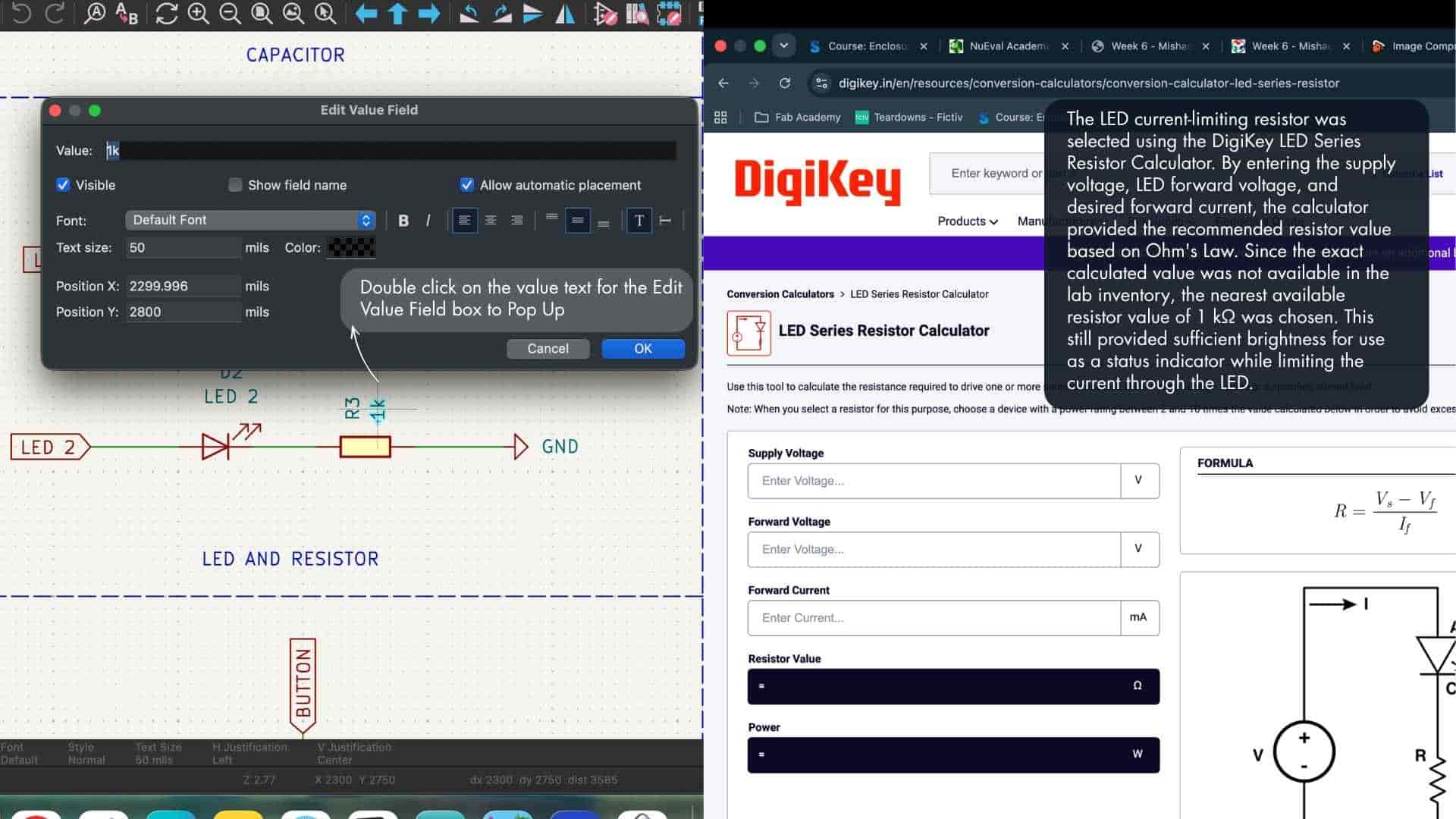
Summary: A UART connector was added to expose the TX and RX pins of the XIAO RP2040, enabling serial communication with external devices such as computers or other microcontrollers. A decoupling capacitor was placed between the 3.3V and GND lines to stabilize the power supply and reduce electrical noise near the microcontroller.
A decoupling capacitor is not a different component type. It is simply a capacitor used for a specific purpose in a circuit. The difference lies in function and placement, not in the physical device.
All decoupling capacitors are capacitors, but not all capacitors are decoupling capacitors. The term decoupling describes the function in the circuit, not a different device.
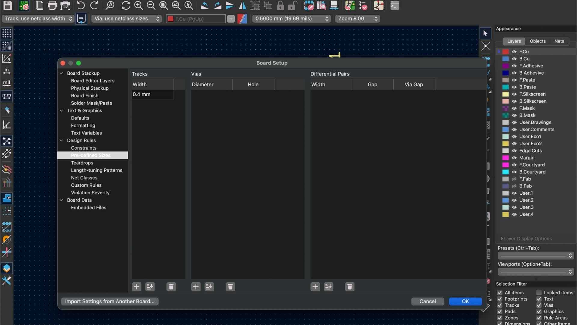
Setting PCB Constraints
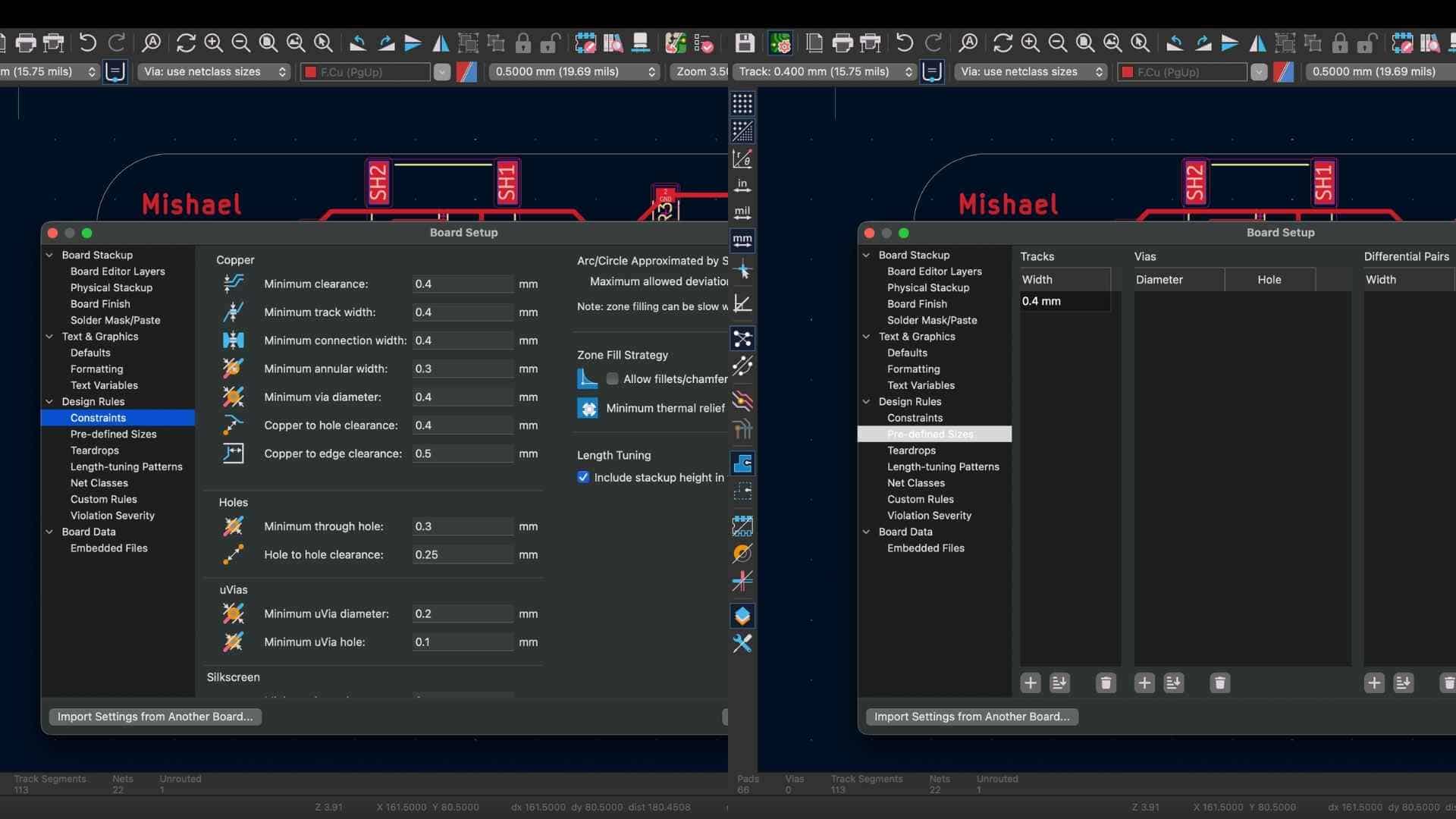
Before starting the routing process, I configured the board constraints in KiCad. These constraints define the minimum manufacturing limits that the PCB must follow during routing.
The settings were configured in Board Setup → Design Rules → Constraints.
Key parameters included:
These values were chosen to ensure that the traces could be reliably fabricated using the available PCB milling process. Setting these constraints beforehand helps prevent routing traces that are too thin or too close together, which could cause manufacturing issues.
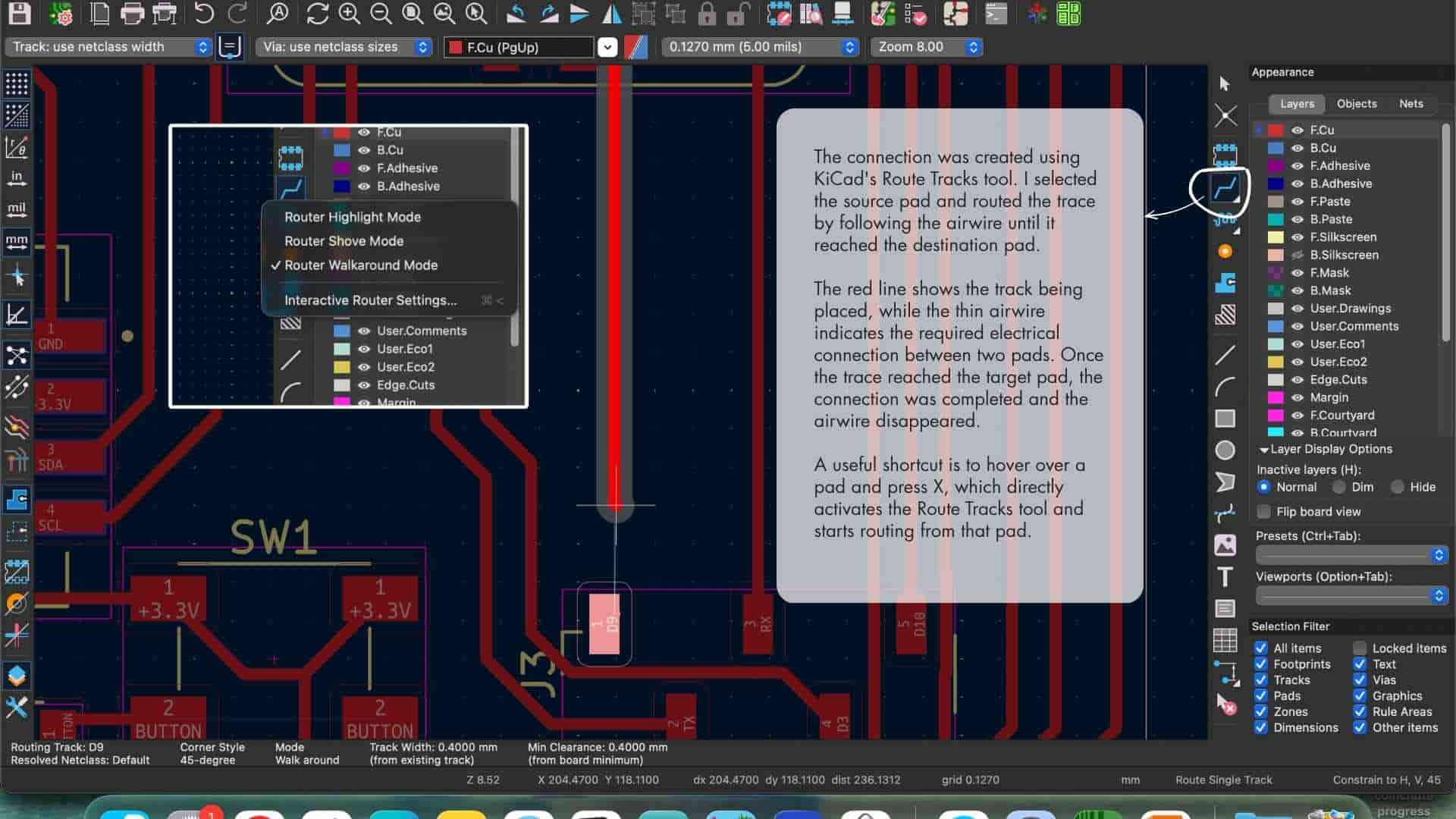
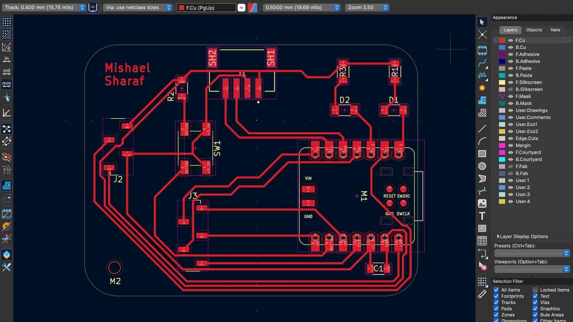
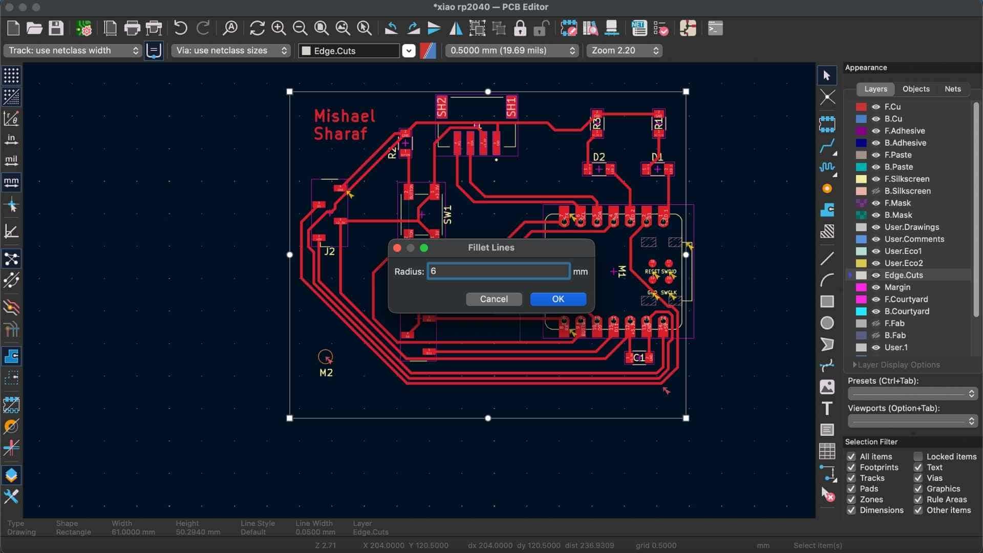
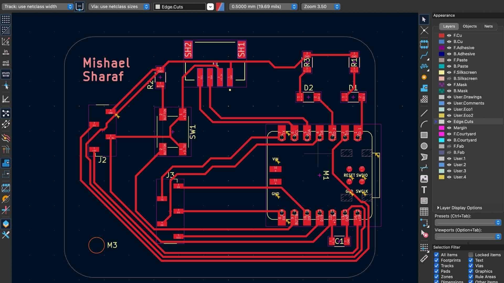
PCB Layout and Routing

After assigning footprints, I moved to the PCB editor and began arranging the components on the board. Component placement was done first to minimize trace crossings and keep related elements close to each other. Some placement considerations included:
Once the components were placed, I began routing the traces. During routing, I prioritized certain signal connections before others. The communication lines were routed first to ensure clear and direct paths.

Priority was given to:
These signals are important communication interfaces and routing them first helps avoid unnecessary bends, crossings, or long paths that might introduce noise or complicate the layout. After completing these connections, the remaining traces such as:
were routed around the existing signal paths. All traces were routed using a 0.4 mm track width, maintaining the spacing defined in the board constraints.
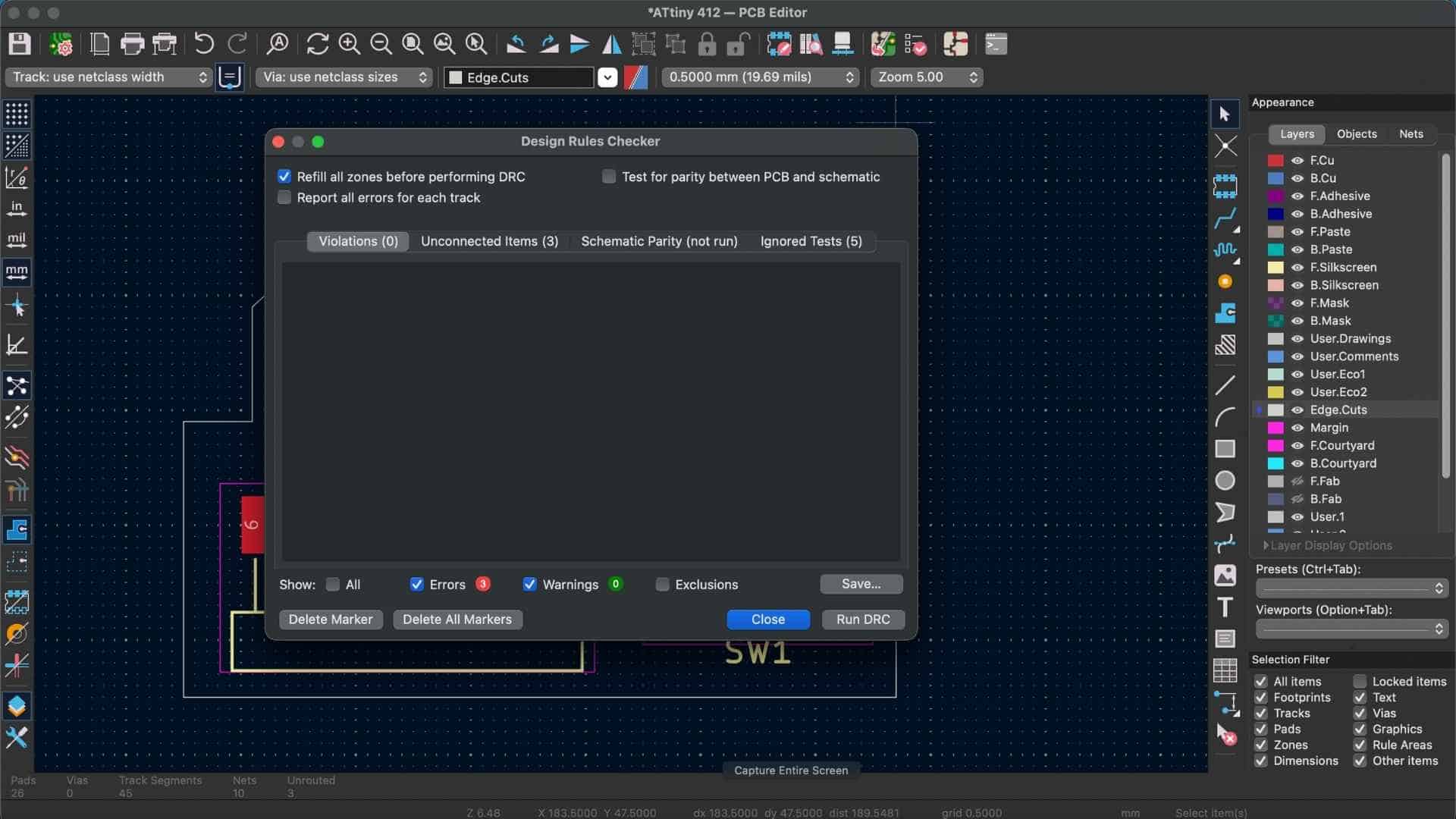
Design Rule Check (DRC)

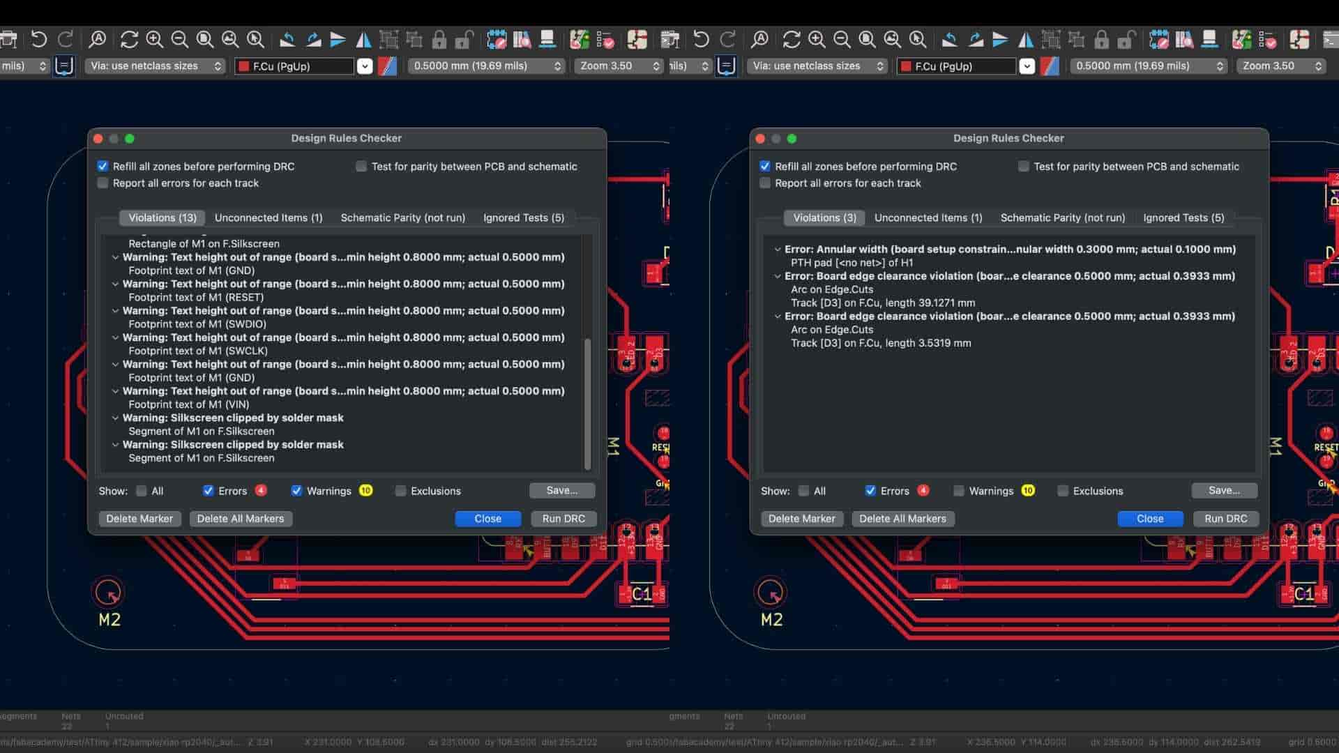
After routing, I ran the Design Rule Check (DRC) to verify the physical layout.
Some warnings and errors appeared, including:
These were resolved by adjusting trace placement, clearances, and text parameters until the board passed the checks.

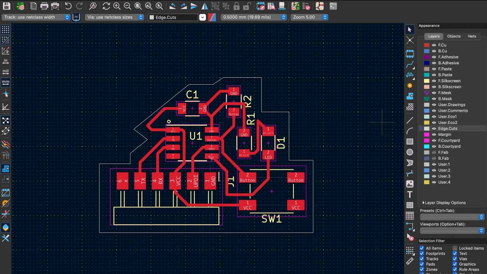
Final PCB Design
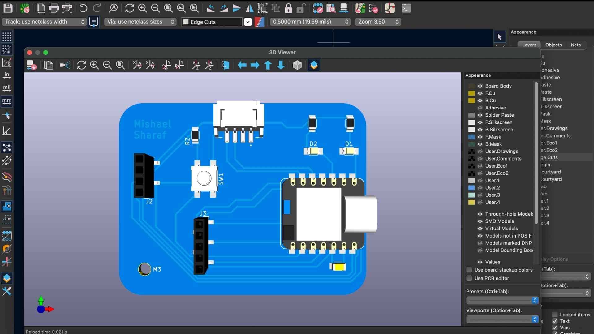
3D Preview
Finally, I inspected the board in KiCad’s 3D Viewer. This helped confirm:
The 3D preview provides a useful sanity check before exporting fabrication files.
Hero Shot
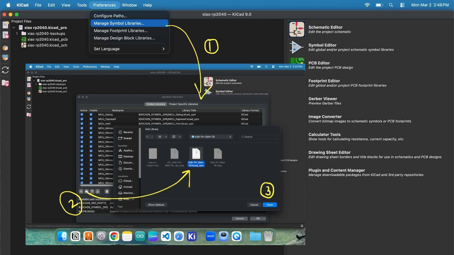
Downloading Symbols and Adding Them to KiCad Library
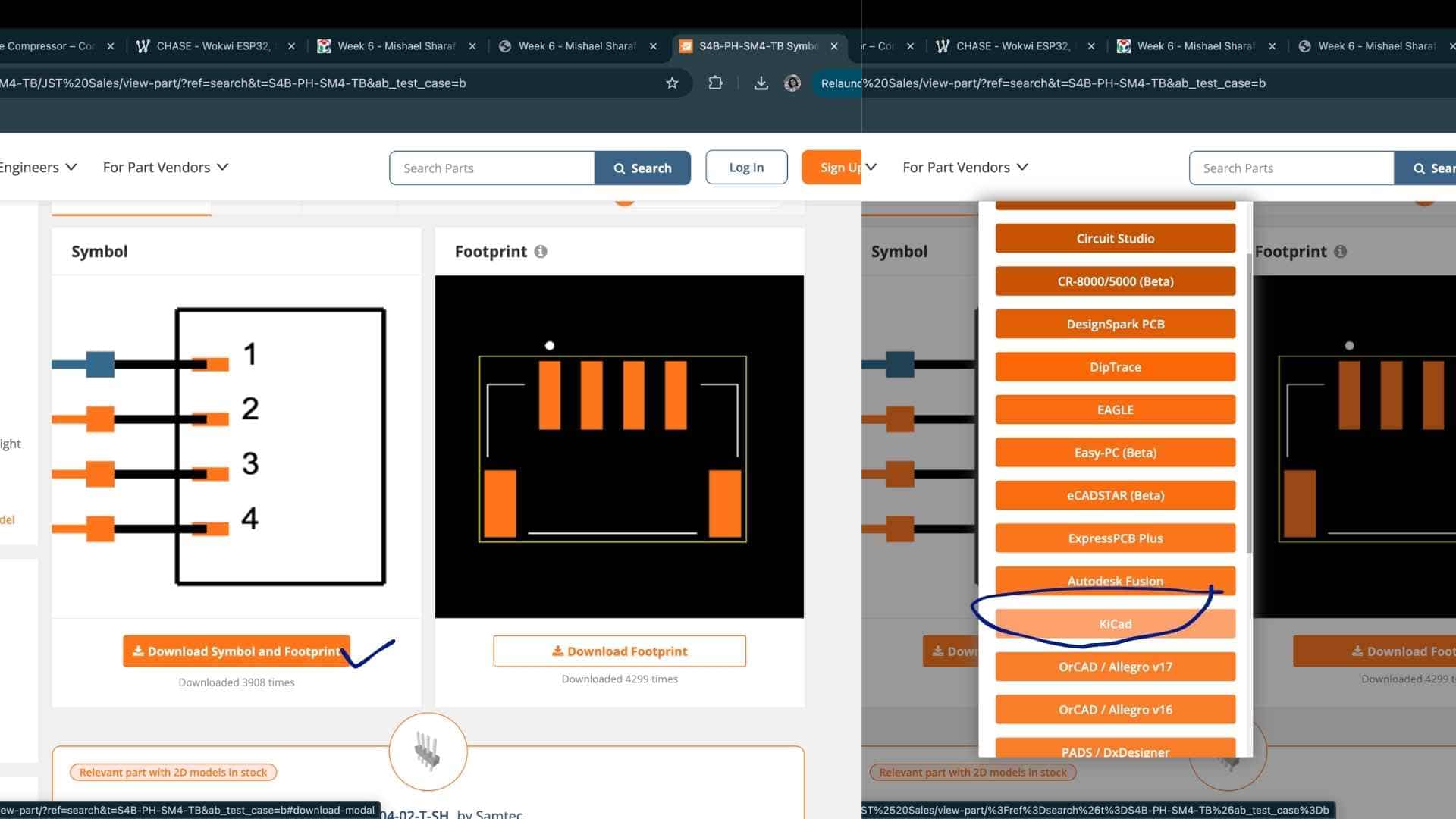
Find and download the component CAD files
Open SnapMagic (or similar CAD library site) and search for the component using its exact part number (example: S4B-PH-SM4-TB).

Steps:
You will typically get files such as:
Add the symbol library to KiCad
Open KiCad main window: Preferences → Manage Symbol Libraries
Steps:
Select:
The symbol is now available in the schematic editor.
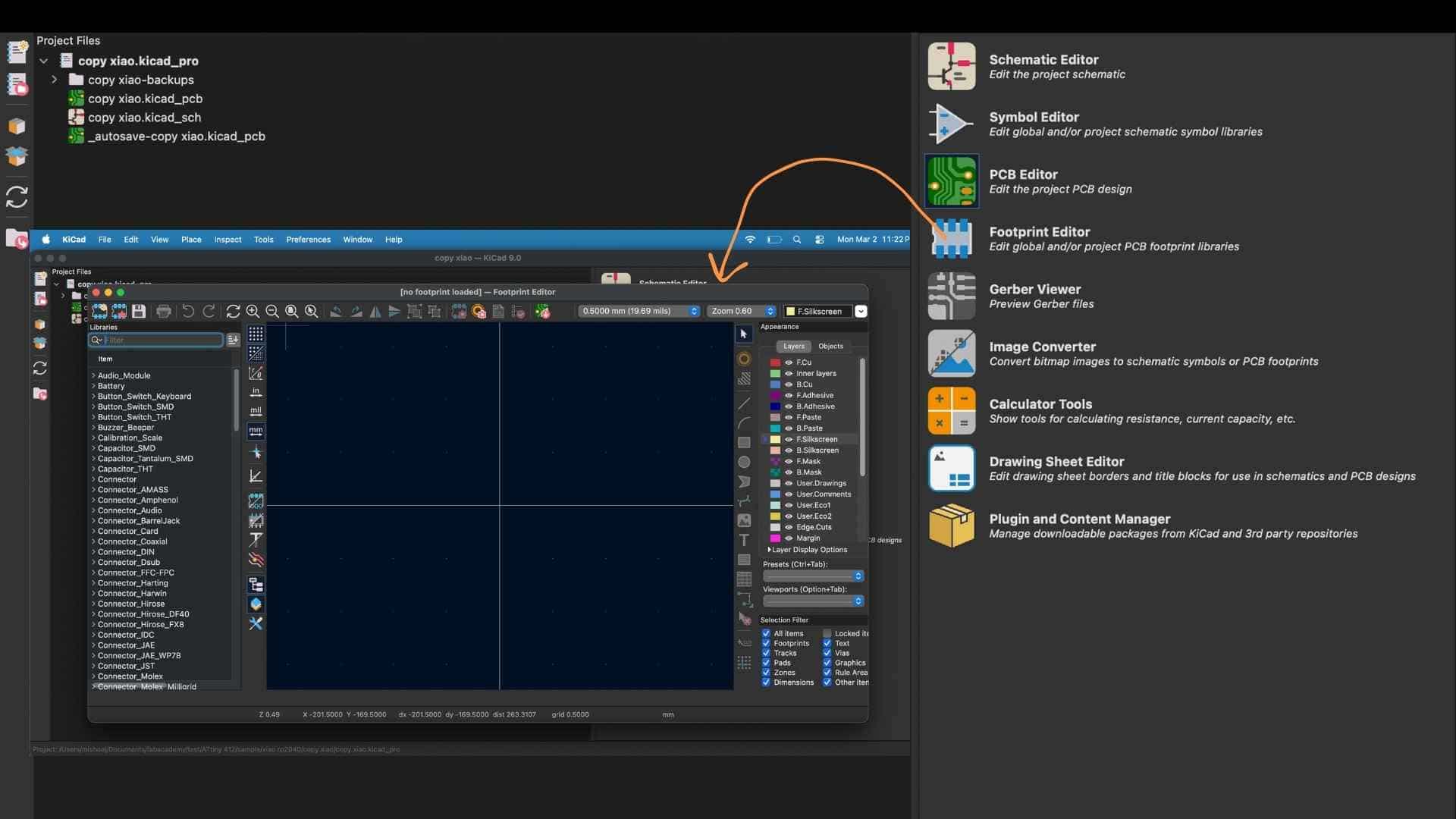
Add the footprint library to KiCad
Open: Preferences → Manage Footprint Libraries
Steps:
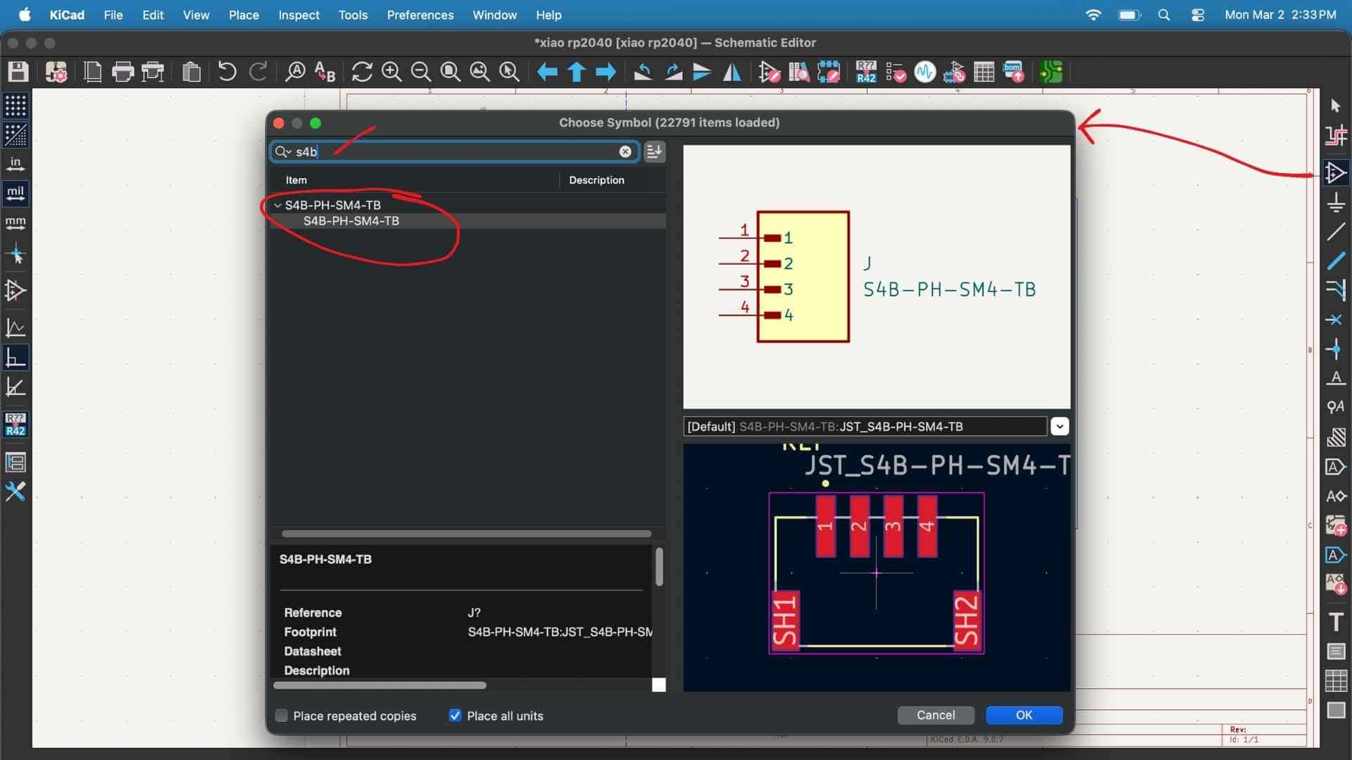
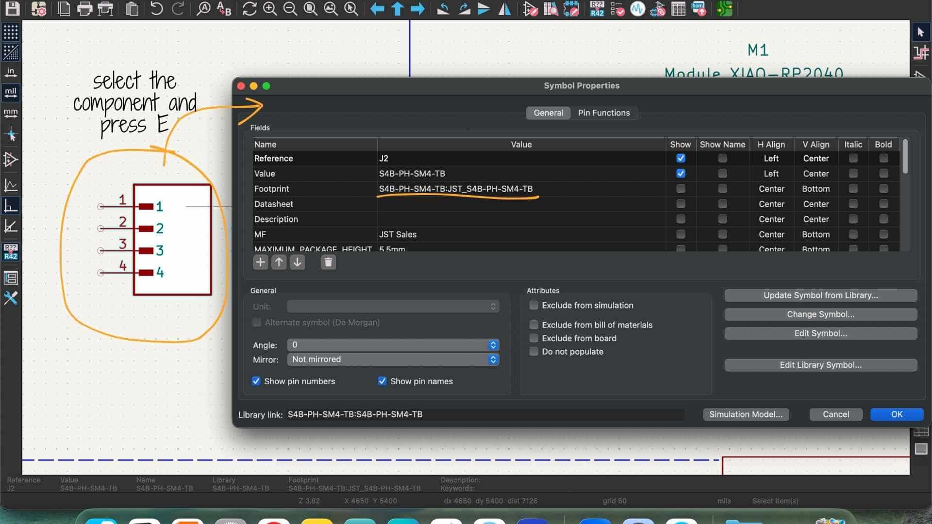
Use the symbol in schematic editor
Steps:
Adding a STEP File to a Symbol in KiCad
In KiCad, a STEP file is not added to the symbol library. A STEP file is a 3D model, and it is attached to the footprint, not the symbol. The correct flow is: Symbol → Footprint → 3D Model (STEP)
Open Footprint Editor
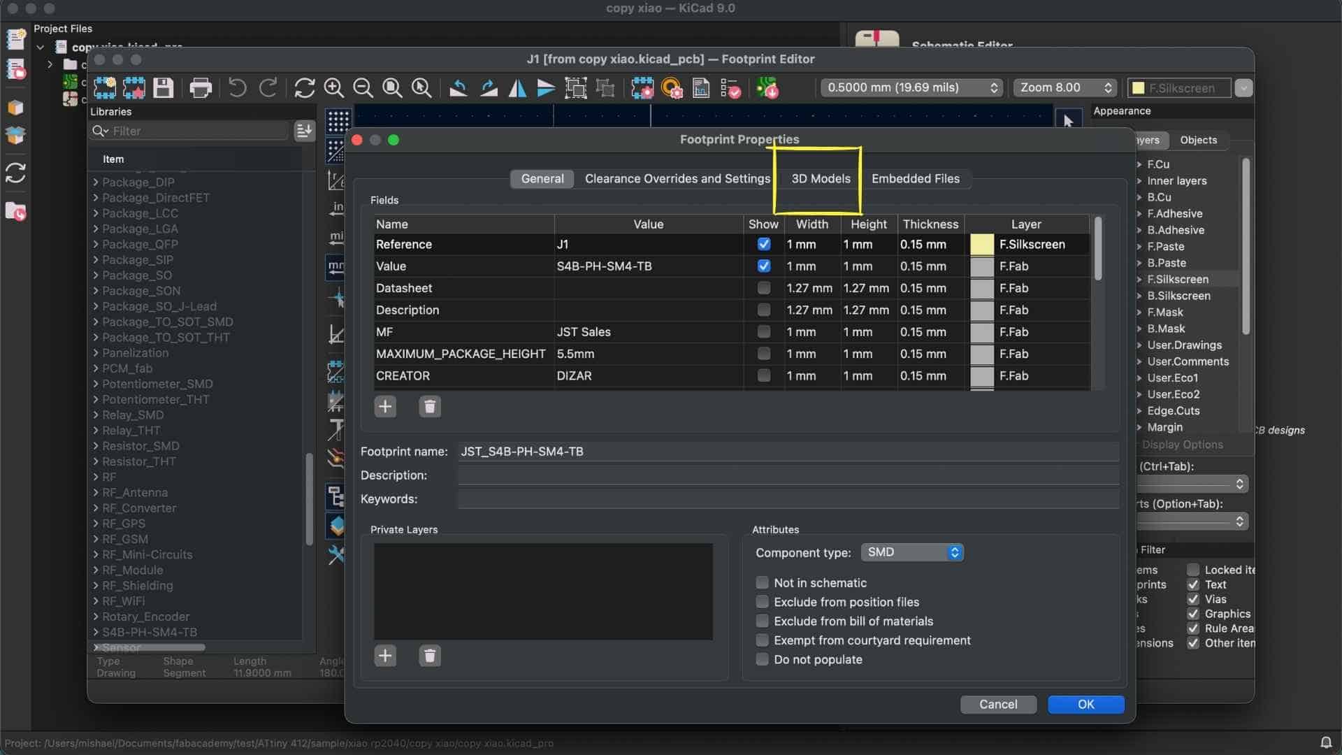
Open Footprint Properties
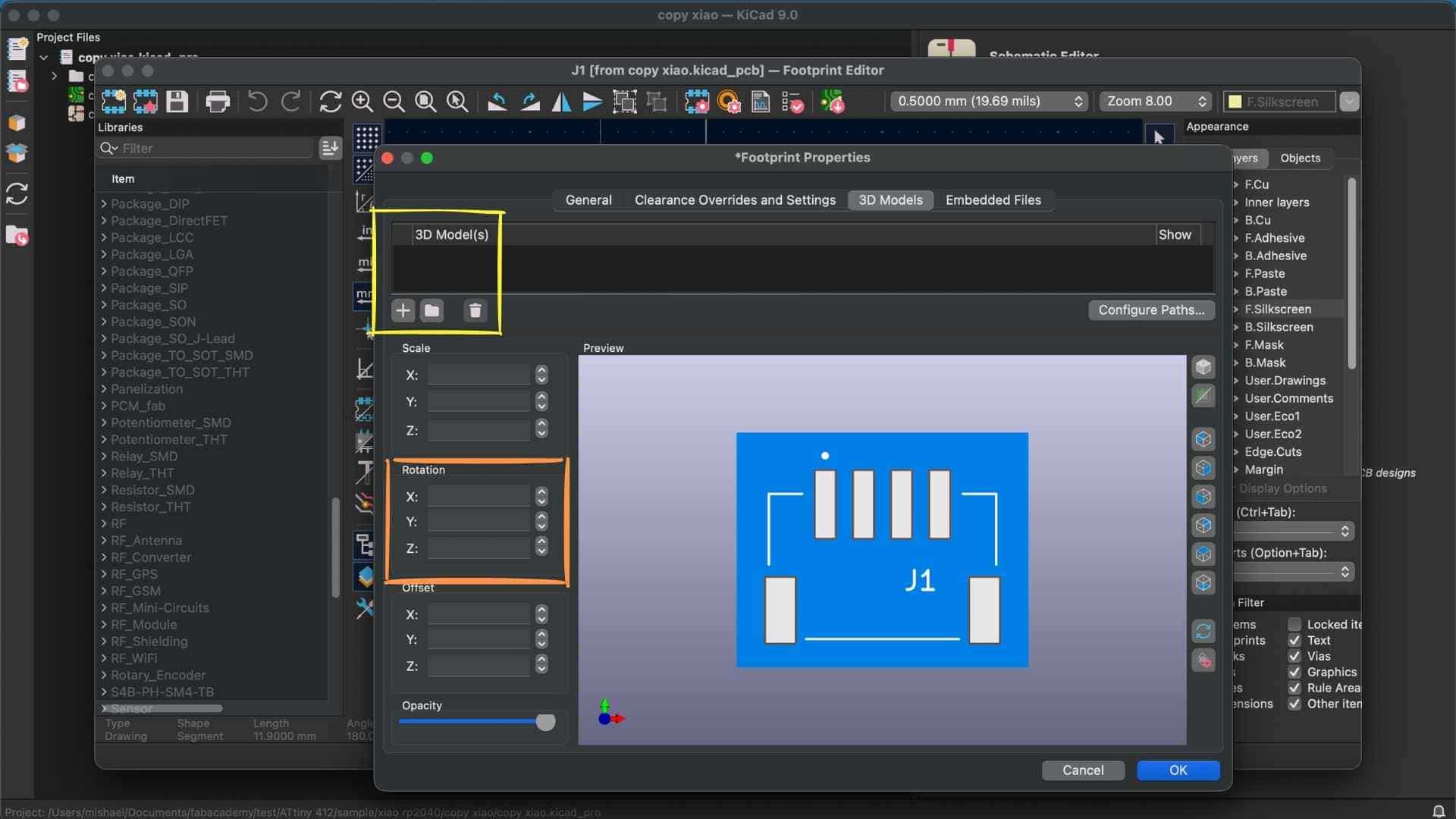
Add the STEP File
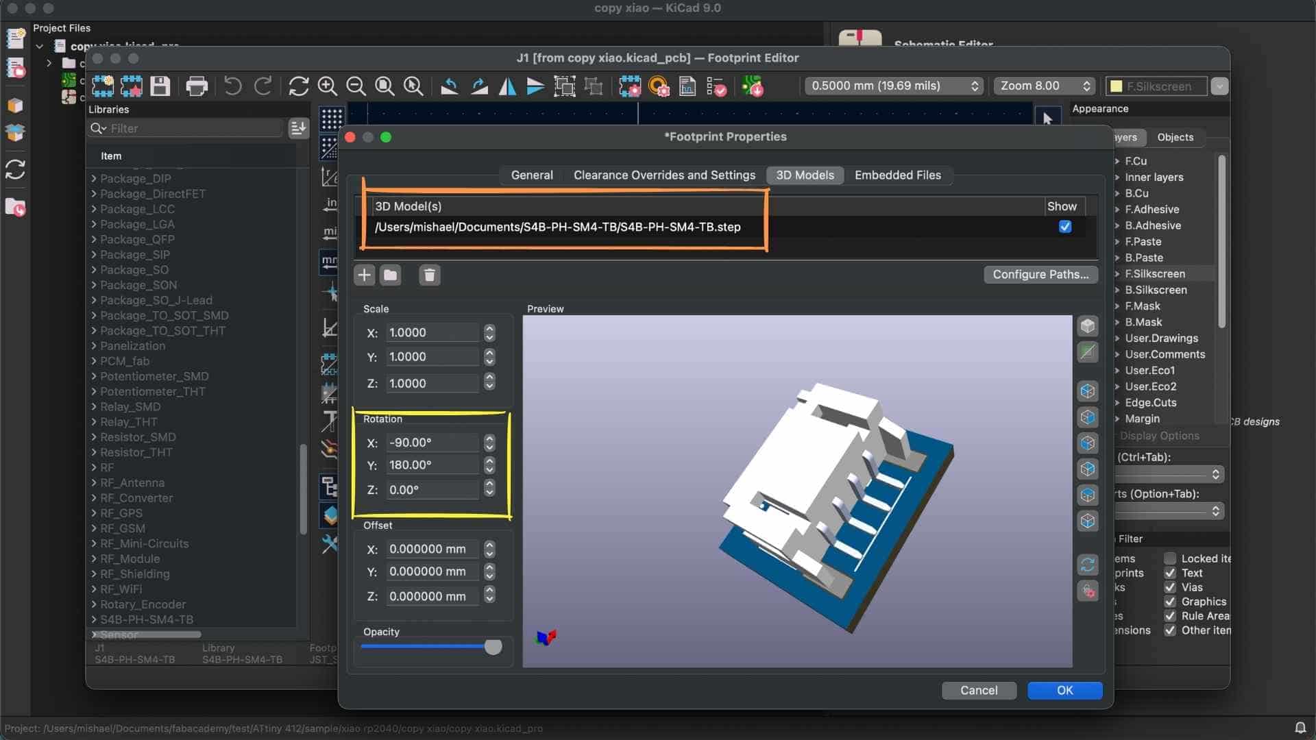
Adjust Model Alignment (Important) After adding:
Save to Library
Reflection
This week felt a-maze-ingly overwhelming, beginning with brushing up on electronics concepts I had not revisited since school, and continuing through the process of drawing copper traces between the XIAO and the various components on the board. At times it felt like being stuck in a never-ending loop with no light at the end of the tunnel.
Although we were told that there is an option to auto-route the traces, I am apparently the kind of person who finds meaning in suffering and chose to route everything manually. The process often felt like being trapped in one of those SpongeBob “eternity” moments, wandering through traces and clearances with a mild sense of hopelessness while trying to avoid crossings and maintain the design constraints.
In the end, the effort was worth the trouble. The process of designing, routing, and validating the PCB helped me learn a number of new concepts and gave me a much better understanding of how electronic circuits translate into a physical board.