INTRODUCTION
Over the last two weeks, I have been splitting my attention back and forth between our amazing group project and chipping away at my final project, the PAK system. In this week, I finally assembled what I could call the very first functional prototype of the PAK, with all of the bells and whistles in tact, just... not very pretty to look at.
If I'm being honest, I pictured myself a little farther along in this development at this point. I think I unrealistically thought I would have a lot of the subsystems of my design figured out - or at least closer to the finished product. Right now, all of the pieces don't play nice with each other, but they are all there. Let me break it down.
[x] Show progress in documenting all previous assignments
[x] Show progress on your final project idea/s and planning
[x] Made a schedule for remaining tasks
[x] Meet with your local and global instructor - Hi Henk! :)
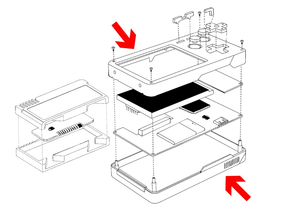
THE PAK SYSTEM
Before we talk shop, let me properly define again what it is that I'm actually trying to make for my final project. I am creating a "dumb" device that requires its user to be intentional with its interaction. The device operates like a smartphone, but takes the form factor of an old Game Boy, where each application runs on it's own dedicated cartridge. The user must decide which cartridge they want to run. The plan is to develop the device itself and anywhere from 2-8 cartridges for the device depending on my time and effort in the coming 8 weeks. The first cartridge will be a simple pomodoro timer that I can use to help myself take breaks when I'm locked in on a passion project. You can read more about the other cartridges I have planned on my final project page.
Development can be broken down in to several subsystems that I need to focus on, each independently, but through each iteration I can get them closer and closer to system integration.
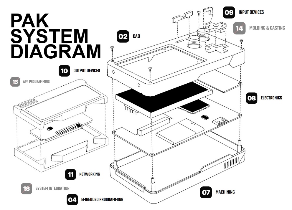
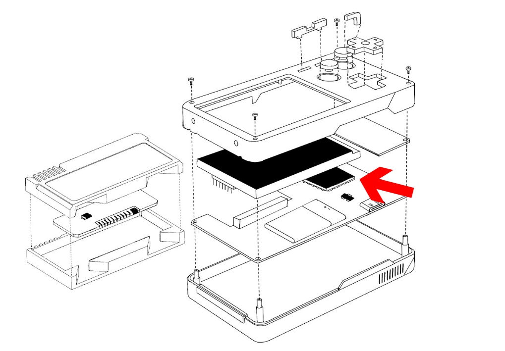
➔ Motherboard PCB
➔ Control System PCB
➔ Cartridge PCB
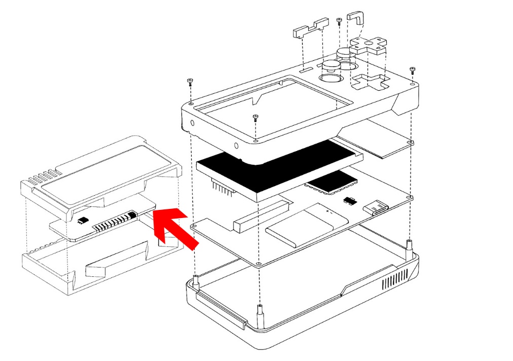
➔ Cartridge Case
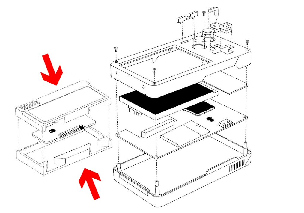
➔ PAK Case
➔ Controls
➔ Operating System
➔ Cartridge Software
➔ UI/UX
This is less of a subsystem and more of a harmony of many of the above, outward facing subsystems, notably the main unit and cartridge cases and the two levels of software described. Being able to create a really sound and consumer-grade device that has a polished user experience is one of my main goals of this project, so I really hope I'm able to get the other items completed to a level that allows me to work on this polish more.
PROGRESS & PLANNING
Let's quickly recap where we're at for each of the above sub-systems and then we can develop a plan of attack for progressing.
➔ PCB Design

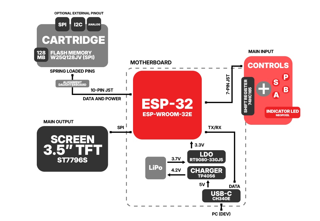
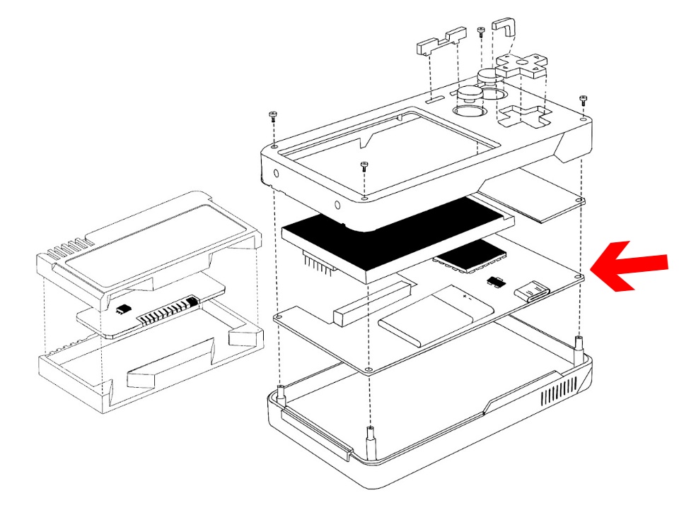
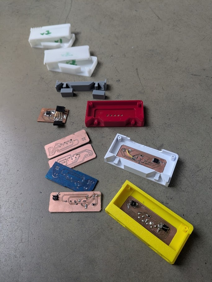
I have milled several boards over the past couple weeks, learning more about electronics design in each iteration. I naively began development in Week 6 and 8 by trying to mill out a "dev kit" on a single, very complex double-sided board. I wrote about all of the issues I ran into in depth in my week 08 documentation. After these learning opportunities, I made the decision to temporarily split up the motherboard into several smaller boards that I could independently mill, test, and most importantly: replace if anything broke. This would help me get closer to a device I could actually start developing on, rather than spending weeks trying to get a single board working (that could end up breaking anyways). Doing things this way helped me learn more EDA and practice my soldering skills in addition.
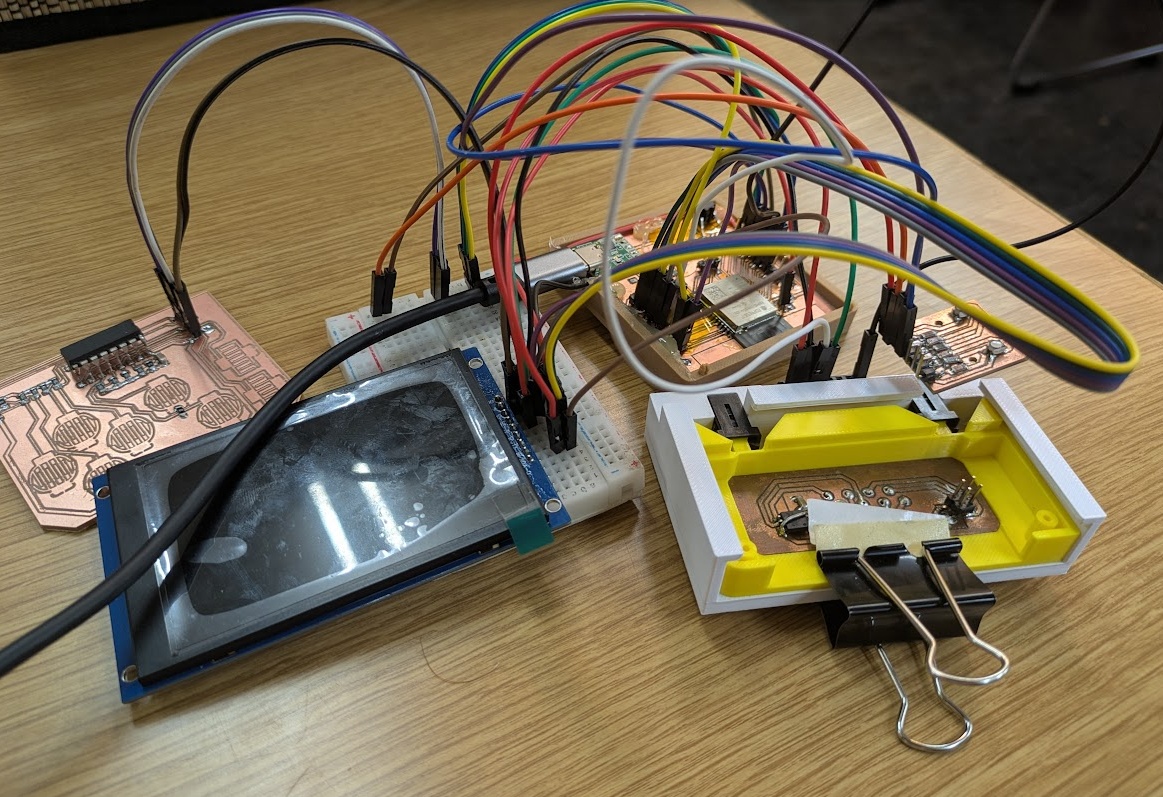
At the time of writing, I have functional (albeit not system integrated) for the main motherboard; which houses the ESP, power delivery (just over USB, no battery), and 21 pin headers that connect to the other boards; the cartridge board which uses my old pogo pin design (bodged together with a literal binder clip); a D-pad/button/shift register board; and a board that houses two RGB leds, although I am only hooking up to one. The whole thing isn't pretty - and I know it's literally a bunch of spaghetti on a breadboard - but it works right now, and that makes me happy and confident to move forward.
With this little dev kit I was able to test all of the pins for my final layout. I've settled on this pinout, and hopefully it does not need to be changed.
| ESP Pinout | Plugged into |
|---|---|
| 1 / GND | GND Plane |
| 2 / VDD | Connected to the LDO, decoupling capacitors and other 3.3V requirements |
| 3 / EN | Connected to the EN switch to ground (with resistor and capacitor in parallel) |
| 4 | Unconnected - in final board have 2x 100k ohm resistor divider for battery chk |
| 5 | Unconnected |
| 6 / GPIO35 | Cartridge External (reserved, input only, ignore for now) - Analog input |
| 7 / GPIO34 | Not Working |
| 8 / GPIO32 | Shift Register Clock |
| 9 / GPIO33 | W25Q128JV CS (Pin 1) |
| 10 / GPIO25 | RGB LED (R) - Common Anode |
| 11 / GPIO26 | RGB LED (G) - Common Anode |
| 12 / GPIO27 | RGB LED (B) - Common Anode |
| 13 / GPIO14 | Shift Register Latch |
| 14 / GPIO12 | Cartridge External - Strapping pin, 10K pull down to ground |
| 15 / GND | GND Plane |
| 16 / GPIO13 | Unconfirmed - EXT Cartridge I2C SCL |
| 17 | Unconnected - Internal Flash Protection |
| 18 | Unconnected - Internal Flash Protection |
| 19 | Unconnected - Internal Flash Protection |
| 20 | Unconnected - Internal Flash Protection |
| 21 | Unconnected - Internal Flash Protection |
| 22 | Unconnected - Internal Flash Protection |
| 23 | Unconnected |
| 23 / GPIO15 | Cartridge External - Strapping pin, 10k pull up to 3.3V |
| 24 / GPIO2 | Cartridge External - Strapping pin, 10k pull down to ground |
| 25 / IO0 | Connected to IO0 switch to GND and resistor to VDD in parallel |
| 26 / GPIO4 | Unconfirmed - EXT Cartridge Chip Select |
| 27 / GPIO16 | TFT Screen DC |
| 28 / GPIO17 | TFT Screen RST |
| 29 / GPIO5 | TFT Screen CS (SPI) |
| 30 / GPIO18 | SPI CLOCK // TFT Screen SPI_CLK and W25Q128JV Pin 6 (CLK) |
| 31 / GPIO19 | SPI MISO // W25Q128JV Pin 2 (D0) |
| 32 | Unconnected |
| 33 / GPIO21 | Shift Register Q7 |
| 34 / TXD | USB CH340E |
| 35 / RXD | USB CH340E |
| 36 / GPIO22 | Unconfirmed - EXT Cartridge I2C SDA |
| 37 / GPIO23 | SPI_MOSI // TFT Screen SDA and W25Q128JV Pin 5 (D1) |
| 38 / GND | GND Plane |
WHAT'S NEXT?
The final goal of the PAK is to have a board house complete the PCB for me, as I need much more precision and complex wiring to keep everything small and compact. I'm conflicted about sending off a board design too soon, as I'm worried I'll run into issues with the board and need to order it again, costing me money and time. I guess I won't know timelines and cost until I draft one up and get a quote - so my immediate plans should be to create a modular PCB for the motherboard and control system that could theoretically find itself in the final design. The requirements are that I get each board as small as possible, and pay close attention to position of pins for optimal wiring, and kind of most worryingly - integrate the power delivery platform that remains to be tested. My other worry is making sure the custom footprints (so far I have designed 4) will work nicely - as trying to bodge things around a PCB is not fun. But again, I guess I won't know the cost and time of these things until I actually get started.
Lastly, I need to complete the redesign for the cartridge PCB once I determine the edge connector parts either available to me in the lab, or at local shops or online.
➔ Case Design
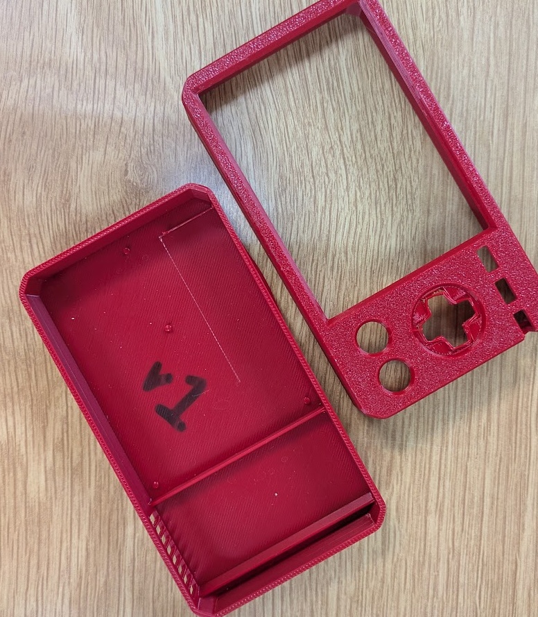
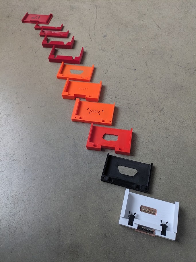
I have a number of prototypes printed from the first few weeks (well a lot of cartridge designs, but really only one design for the PAK itself), mainly just as a way to start getting a feel for the footprint of the finished product. The only part of the design that I have, in theory, completed is the rail/block system for the cartridge slide-in, preventing the user from inserting the cartridge the wrong way. I'd like to stick with the current dimensions I have for all of the printed parts for now, but understanding that I can loosely edit them to make them fit nicely with our internals.
I've also thoroughly tested the push-push mechanism for the cartridge port with off the shelf components ordered from AliExpress. It works very nicely and I seem to have already got the spacing and tolerance dialed in. I just hope it plays nice with the friction/contact needed for the edge connectors.
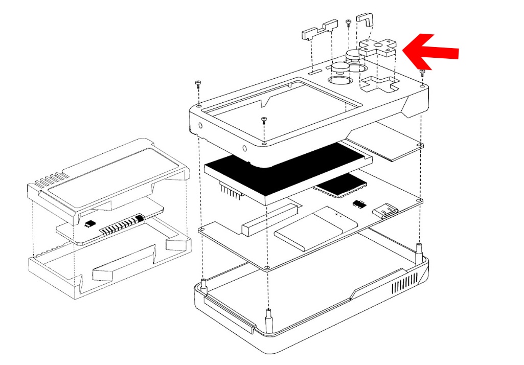
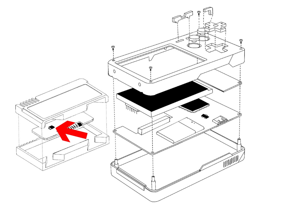
I did some testing of the RGB LED and a 3D printing light pipe back in week 10 to get a sense of how the indicator LED will look. This is something that will likely be revisited towards the end, but getting the location of this light is important on the board, as it should line up with the other system buttons (START and "P") as shown in this image:

The buttons themselves are also an important part of the case. I have only been using off the shelf components up until now, which obviously will not be suitable stock in my final design.
WHAT'S NEXT?
The current prototype is not super transportable, so I think the first order of business is to print a case that at least lets me move around the dev kit without being worried about disconnecting parts or traces getting ripped up.
I am concerned with aesthetics of the final design, but in my experience with Fusion so far, parametric design doesn't play well with final polish when we're tinkering with small details, so the plan should be to first design and print a basic block-like case that can act as the housing/skeleton for the internals and then when we're happy with that footprint design a more aesthetically complete shell using the same footprint and either have it printed in house or shipped off to a print house.
After learning more about molding and casting, develop, design and cast buttons that feel satisfying to use. I'm aiming for softer, rubbery buttons that have a bit of give and playfulness to them over super rigid plastic ones. I'll have more to report on this after I've experimented next week!
➔ Software
Up until this week, I have been writing all of my test software in complete isolation. Each script is basically starts from scratch so I can test the components individually to test if they even work in the first place. Early I decided to use CircuitPython on the XIAO devices for ease of use in flashing (I really can't stand how long it takes to flash a device through Arduino) and for familiarity with Python. I took a one week dive into trying development on C++, but quickly became apparent how far in over my head I would be if I continued down this route. C++ is so difficult to debug and, while I'm sure it will net me better performance, it's simply not worth the effort trying to develop on it if it risks making actual progress. I've made the switch to MicroPython and after doing some research and testing, it feels like the right call for the rest of the project's development.
Now that I have a fully assembled first prototype, I could start developing software with central methods and classes that all scripts can pull on. If I get this prototype in a transportable form, I could in theory just continue writing software on it wherever I have my computer - which would make it very easy to chip away on it over the coming weeks.
WHAT'S NEXT?
Develop a system level object-oriented architecture in MicroPython that can test and debug all of the individual subsystem components and hand off arguments to functions that could be called in cartridge applications. Then we can start fleshing out the skeleton of the UI and tweak it over time. Priority is one creating a good try/except block that catches errors, safely releases the SPI bus (to ensure we don't corrupt the data on our flash memory), and gets our errors on screen instead of just in the serial monitor.
Once I have a debug/system level script running, I can start development on the simple cartridges. I think bare minimum, I need to create the pomodoro application and get it flashed on a cartridge. From there we can look into creating more of the stretch goal cartridges.
Conclusion
The assignment this week asks us to schedule out our remaining tasks. The most immediate action items for the coming weeks seem to be:
- talk to Yuichi about edge connectors for the cartridge, see what my options are
- print a case that lets me move the dev kit around
- complete the redesign for the cartridge PCB (and do a test mill in house)
- design the PCB for the motherboard and control system and ship it off to PCBway
- system level object-oriented architecture in MicroPython
From here, I'm able to develop on the system while I wait for other parts (or for my own learning) to develop. After next week, in completing molding and casting, I should be able to:
- begin developing a design and cast buttons that feel satisfying to use
- print out a placeholder case/interface for these new buttons to my existing dev kit
And then continue development into the third (and beyond) spiral. These tasks align nicely with the assignments each week, so it's easy to assign myself deadlines that align closely to those tasks.
- creating the pomodoro application first, and then more complex apps
- designing and printing a basic block-like case that can act as the housing/skeleton for the internals
- create cartridges with modifications that can house expansion components
And in the final weeks:
- design a more aesthetically complete shell using the same footprint as the block-like case
- polish the UI/UX of the software
- work on the final presentation slide and video, which I'm planning on creating 3D renders for to make it feel a lot like a consumer electronics product reveal