INTRODUCTION
There has not been any other week in this program (so far) that has matched the level of exhaustion and turmoil I experienced this week. Let's get straight to it. There's a lot to share.
[x] Characterize the design rules for your in-house PCB production process: document the settings for your machine.
[x] Document the workflow for sending a PCB to a boardhouse
[x] Document your work to the group work page and reflect on your individual page what you learned
[x] Make and test a microcontroller development board that you designed

[ ] For my students:
You can also read about our group assignment at Fab Lab ESAN here.
PCB Milling
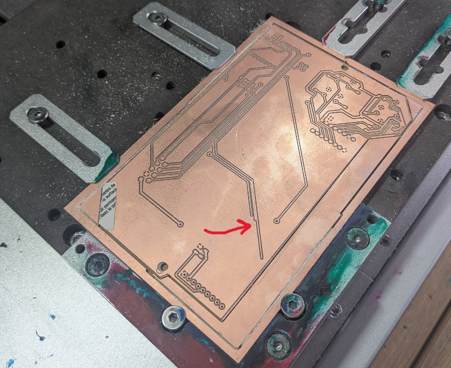
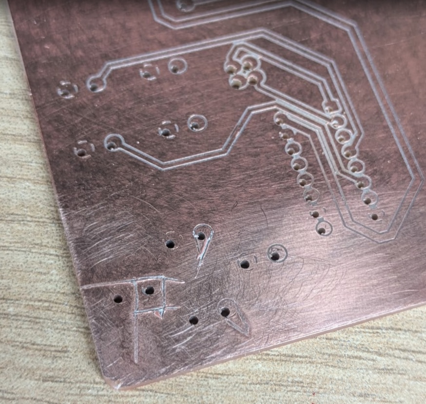
The workflow for PCB design is, in theory, quite simple. Your EDA software (such as KiCAD) can export special files, called Gerber files, that contain the outlines of each of the different layers of your PCB. For PCB production here at ESAN, these outlines simply need to be converted into a toolpath, or G-Code, for our Makera Carvera machine to mill out from a copper FR1 board. The basic workflow for a single sided PCB with no extra bells and whistles runs as follows. I'll walk you through each step here as I did for my first custom PCB:
KiCAD ➔ (export gerbers) ➔ Gerber2png ➔ (export pngs) ➔ Modsproject ➔ (generate .nc files) ➔ Carvera Controller ➔ (mill the PCB)
➔ KiCAD
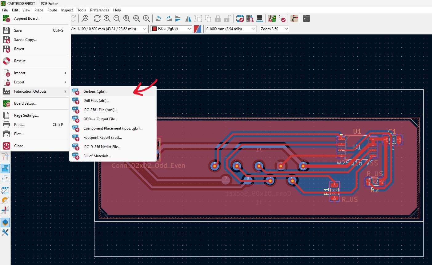
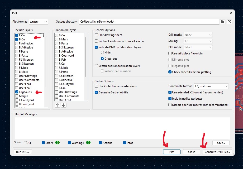
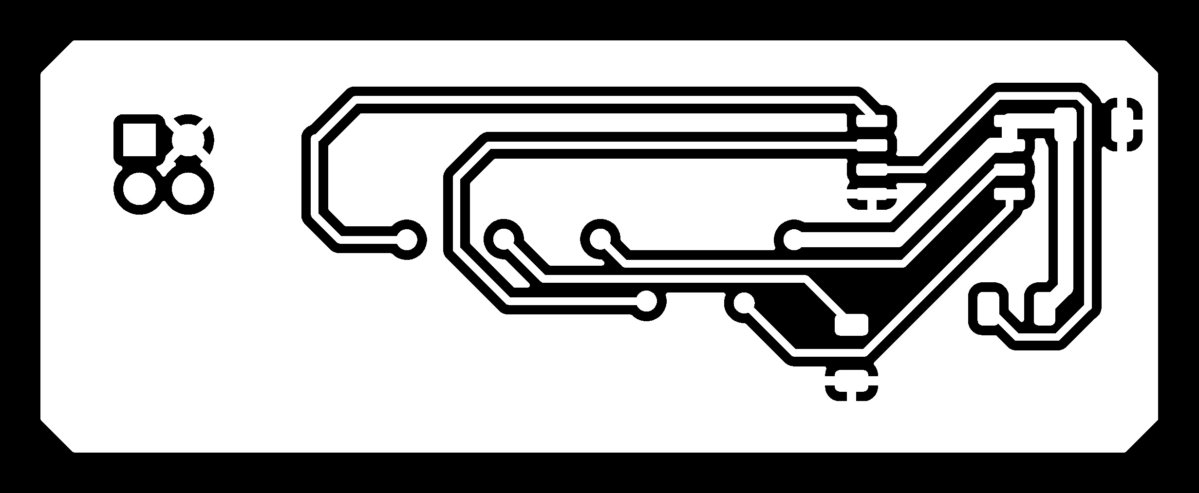
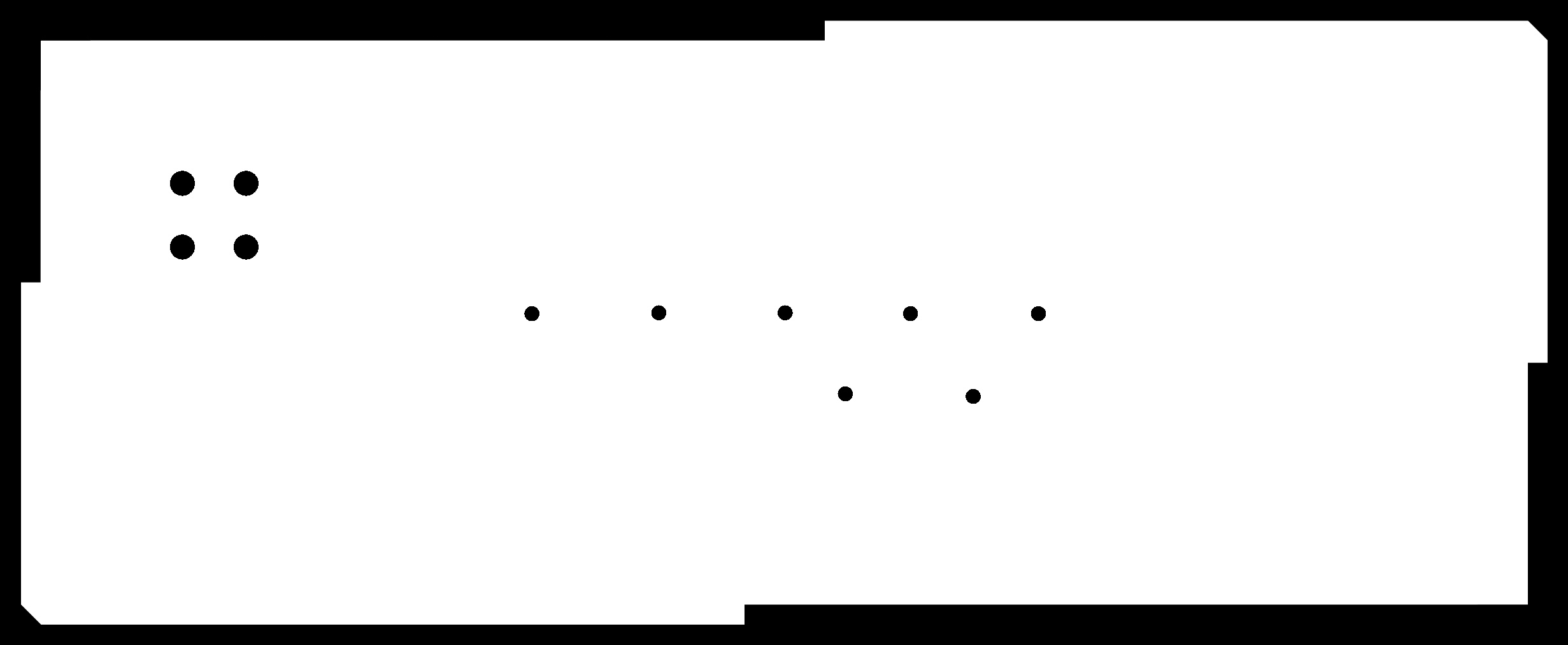
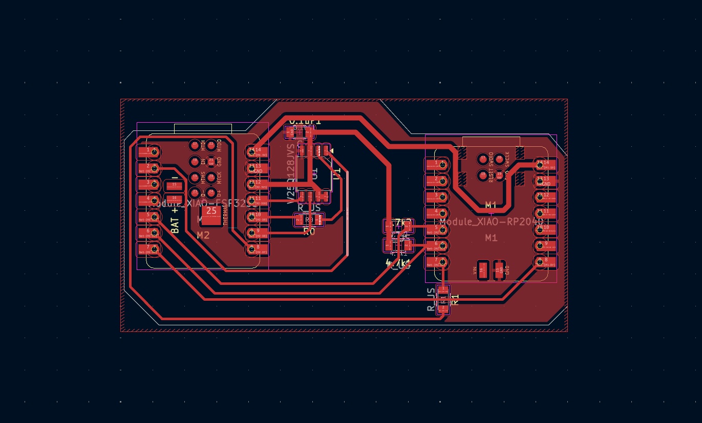
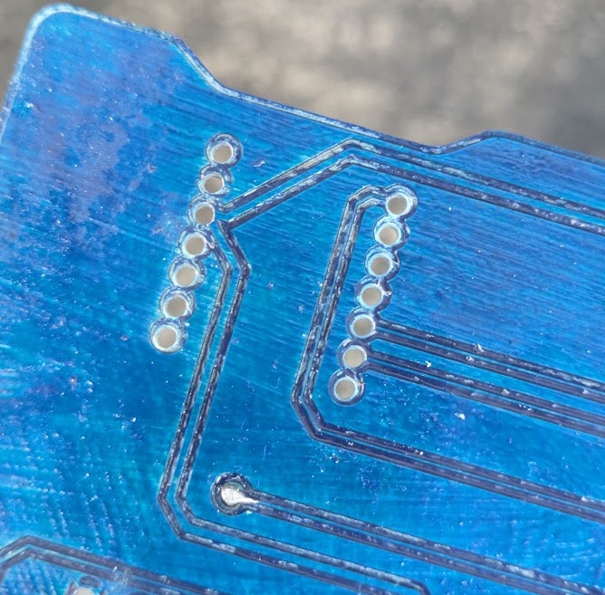
You can read more about how to use KiCAD to design a circuit back in Week 06. Once you're happy with your schematic and PCB layout, head to "File > Fabrication Outputs > Gerber Files". Depending on your PCB design, you may have to export several files here. For a simple single sided PCB with no through hole components, all you need to export is the F.Cu and Edge.Cuts layers, then click "Plot". For my PCB design, I chose to try a double-sided design with through hole components, so I would also need to export the back B.Cu layer and the drill file by clicking "Generate Drill Files..."
You'll be gifted with new files in your project directory. You can see mine here!

➔ Gerber2png
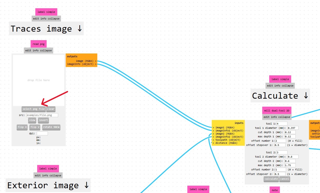
While we could use the software that the Carvera comes with, Makera CAM, it's not super intuitive. Luckily, our friends at Kerala developed a workflow that allows us to generate images from our gerber files, which can be run through modsproject to create an .nc (g-code) file compatible with our Carvera. That doesn't mean Gerber2png isn't without it's own quirks though! To get started, simply drag or open up ALL of your gerber files that you exported in the previous step!
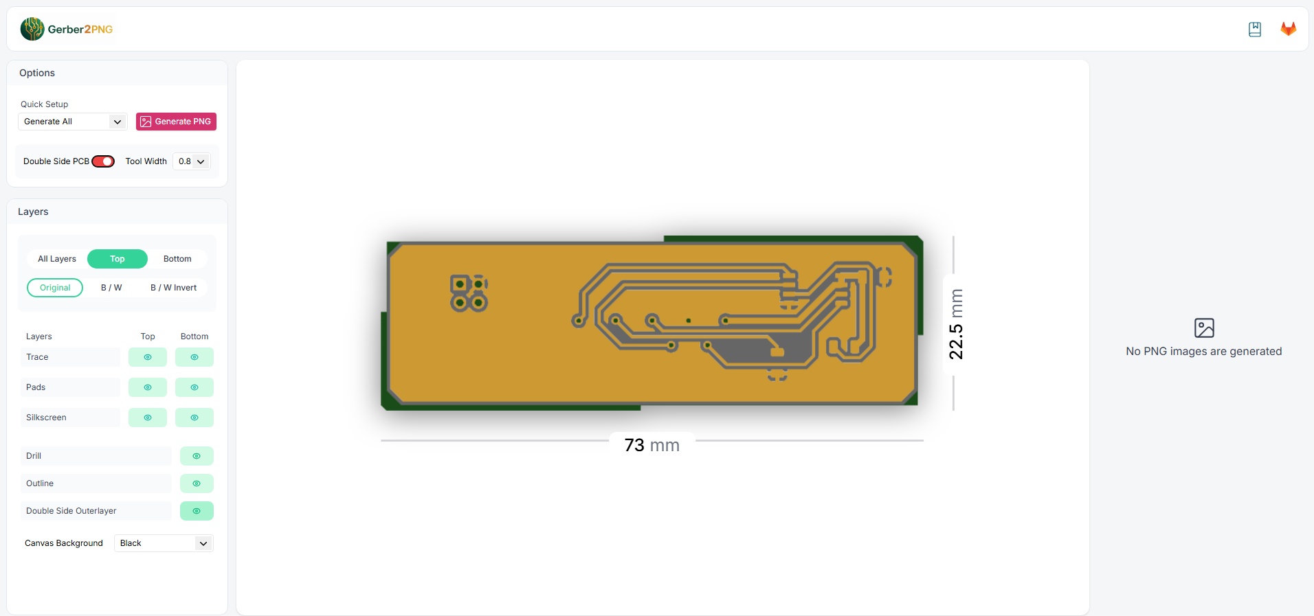
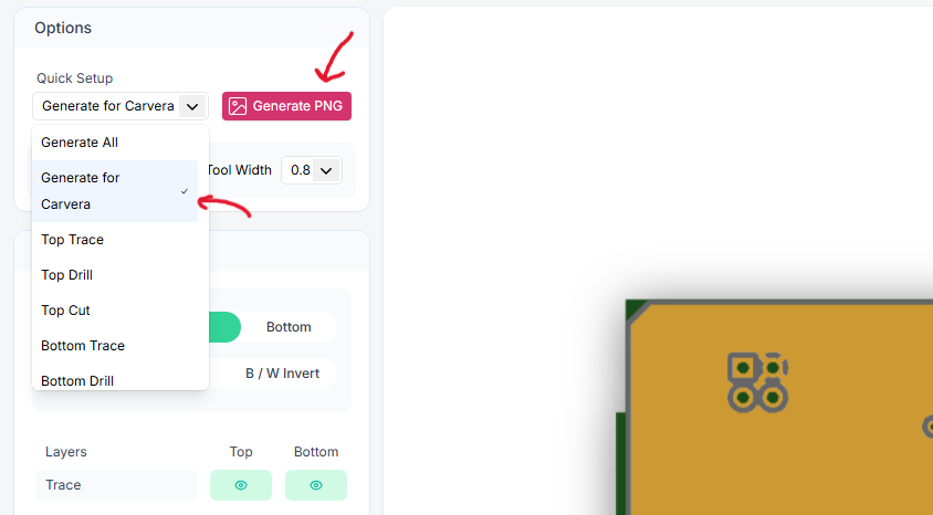
Gerber2Png has a neat little tool that helps you create double-sided PCBs without having to worry about alignment posts or reassigning the home on your mill. It does this by creating a little frame around your PCB's design that lets you pop the board out when you're finished the first side, flip it around to the back, and smush it back into the frame, where it is held in place with friction. I would still highly recommend adding some double sided tape though!
Once you've reviewed your files in the preview, click the "Download All" button in the corner on gerber2png, and you'll receive a zip folder of 4 files.
➔ ModsProject
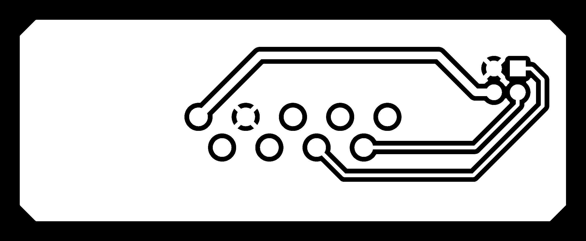
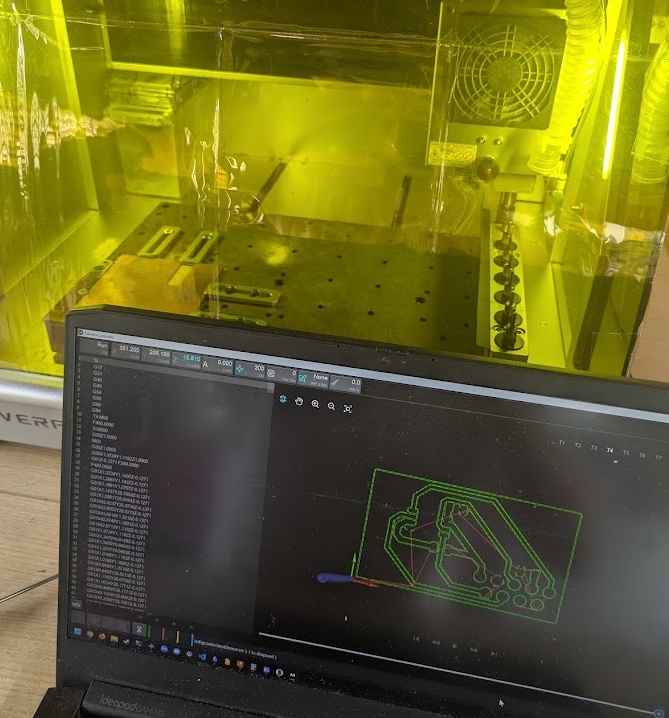
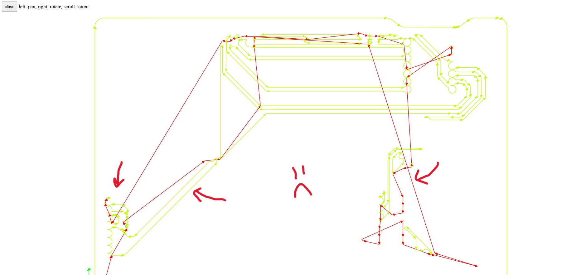
While it would be cool to have a machine take an image file and start cutting things, we still need G-Code to control the motors. Welcoming back our friend from week 03 is ModsProject, another great (albeit quite temperamental) open source tool that can create G-code for all sorts of machines. This one takes some playing around to get right. I found that I had to lie to ModsProject about my tool diameters (as you see me doing here in step 3, changing my tool diameter to something smaller) in order for it to properly detect and plot out the traces I wanted. I have a suspicion that I was having trouble with this due to my KiCAD parameters, so I'm having my mentor Jorge look through my files - I will report back!
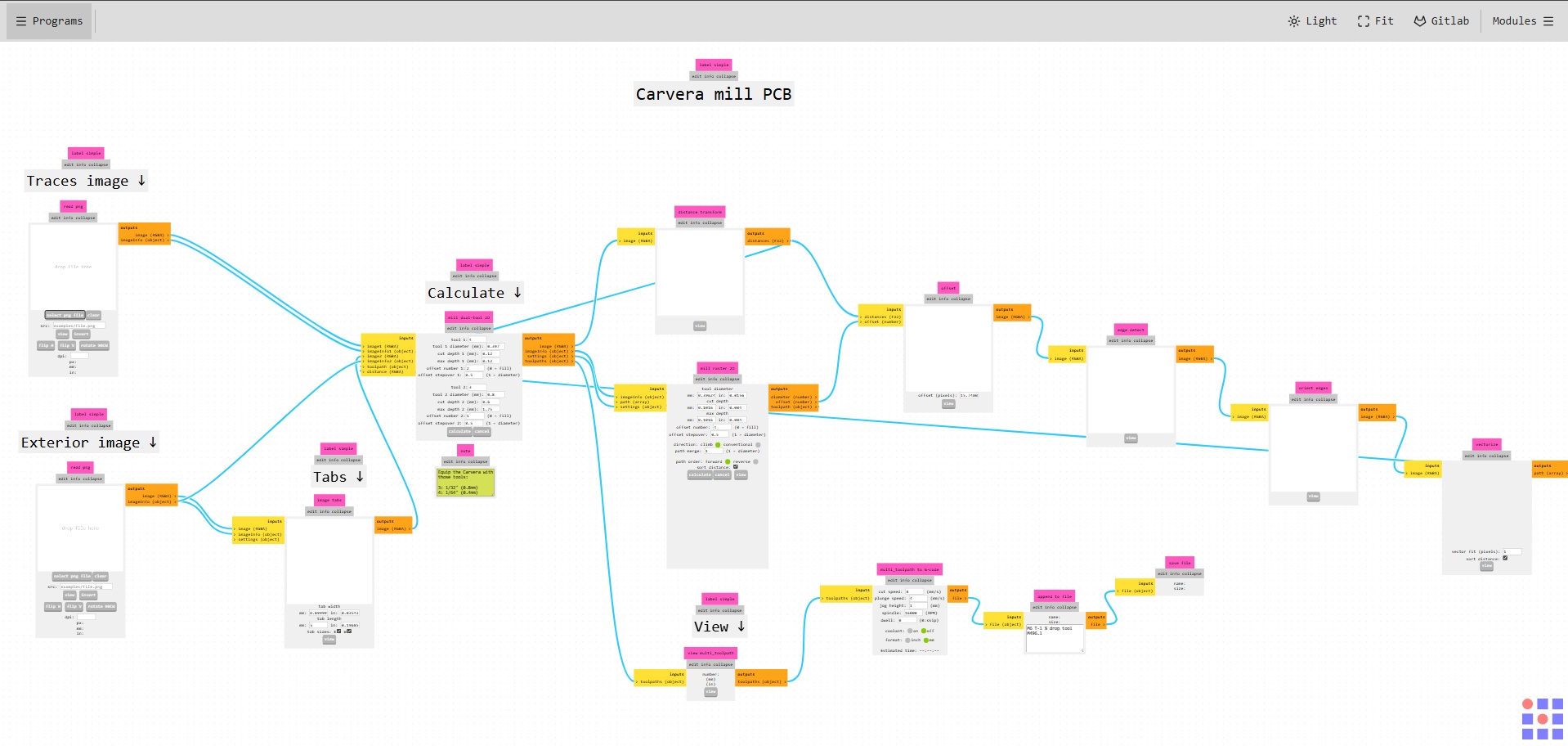
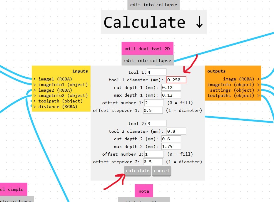
This program in ModsProject works by taking the interior cuts (which would be engraved) and the exterior cuts (which are cut out) and combines them into a single .nc file that the Carvera (which has automatic tool switching) can use to mill your board. My mentor, Jorge, recommended that I still create the files separately though, as the Carvera has a tendency to forget what tool it's using and literally crash.
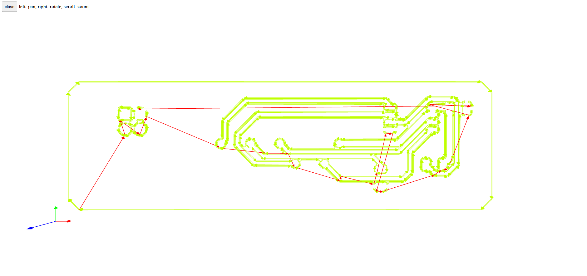
Anyways, import your PNGs, check your tool settings and then click generate. ModsProject will open a new tab to show you (weirdly in 3D) your toolpath and download you a nifty .nc file (which I can only assume stands for nifty cut).
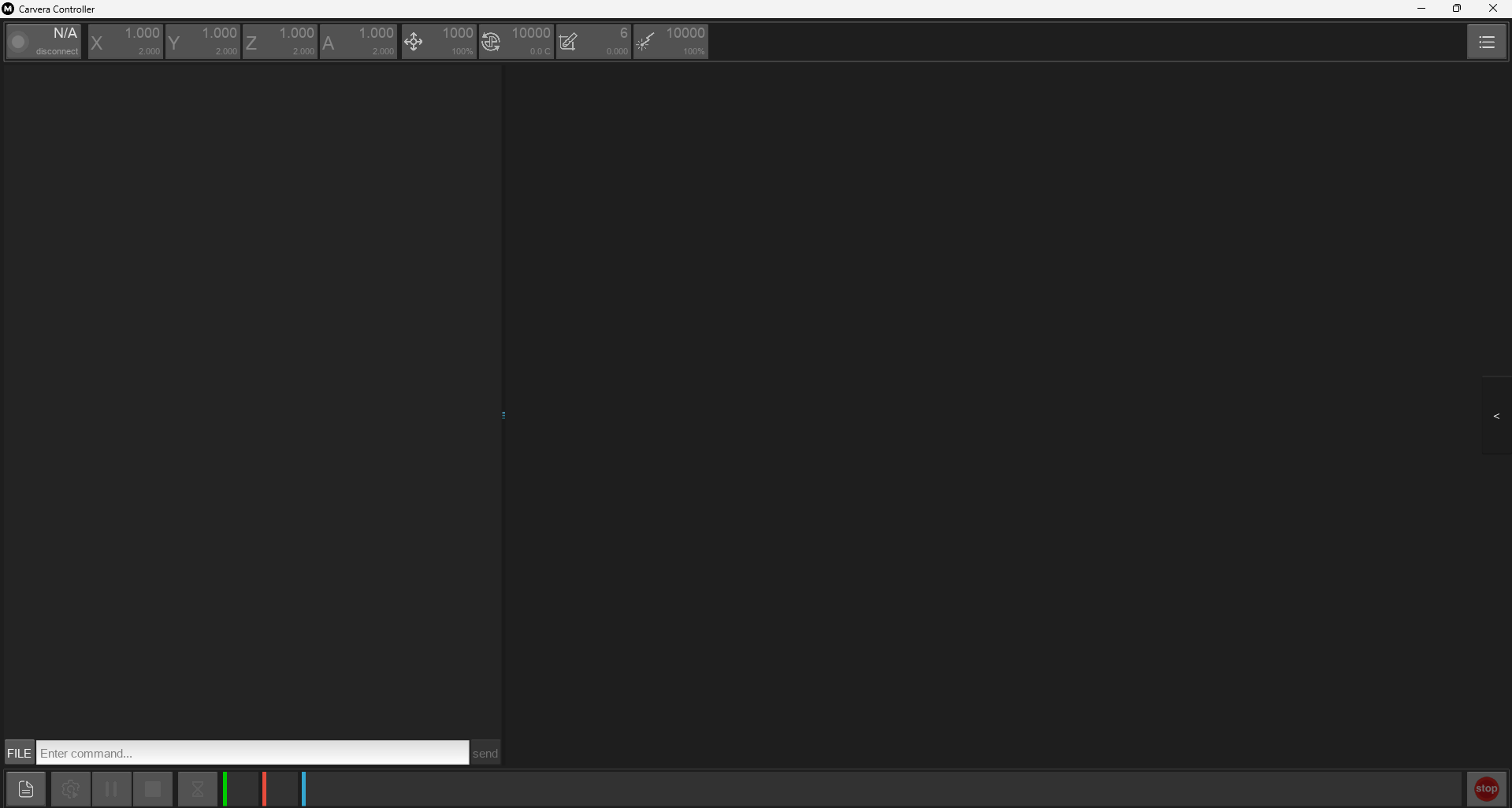
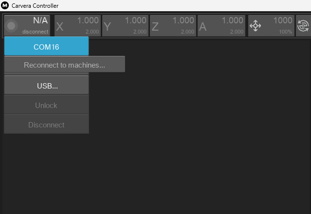
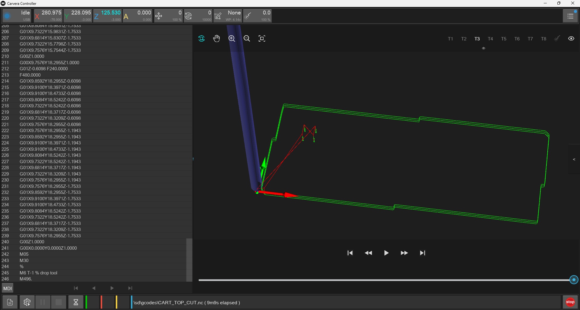
➔ Carvera Controller
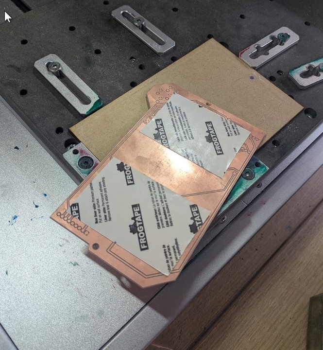
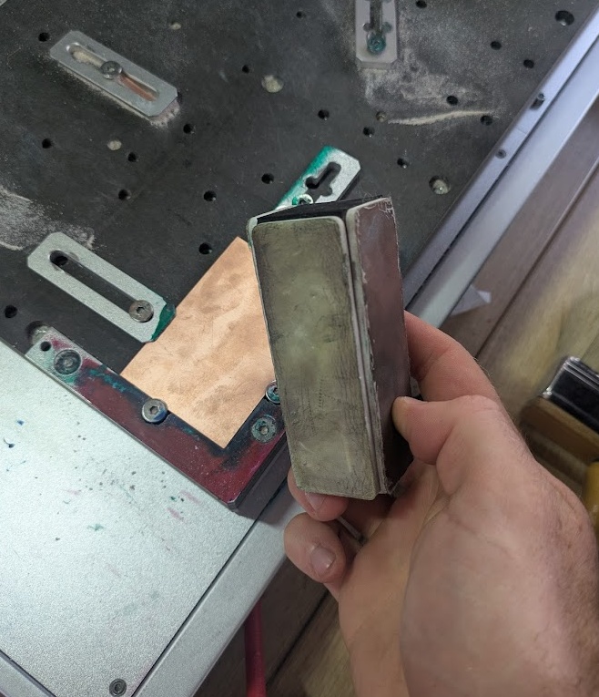
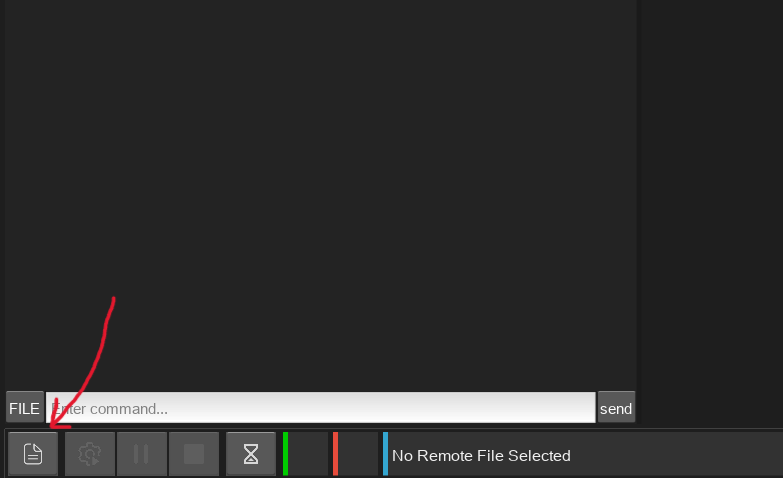
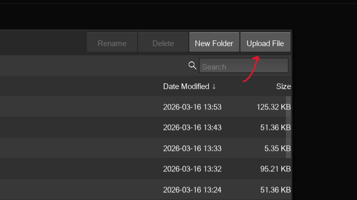
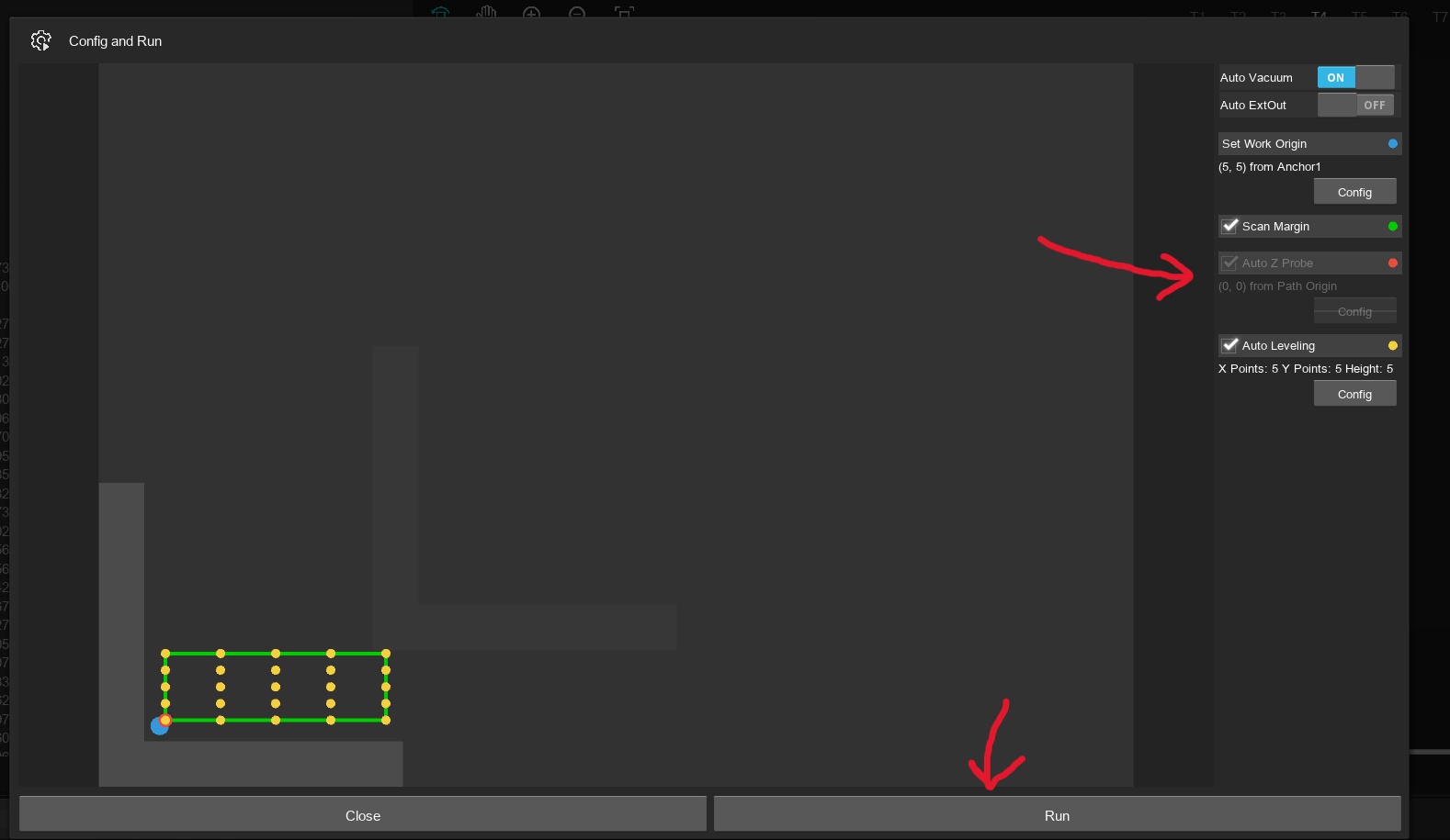
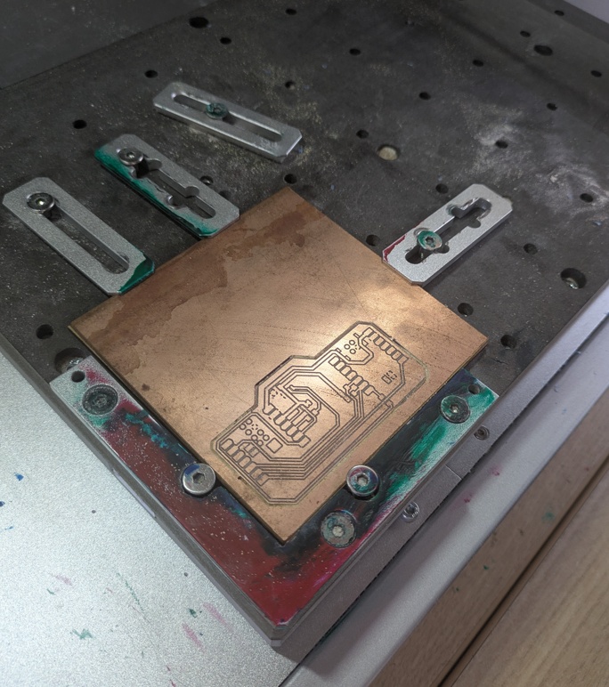
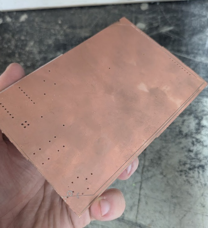
On to our fourth piece of software in the workflow, if you're counting. Carvera Controller is a piece of software that does exactly what it is named to do, it controls the Carvera. You need to upload your .nc to the device itself, and then prepare your workpiece for milling. You'll want to lightly sand your copper piece using a 1000 grit sanding block, then screw down the board (on top of a spoilboard).
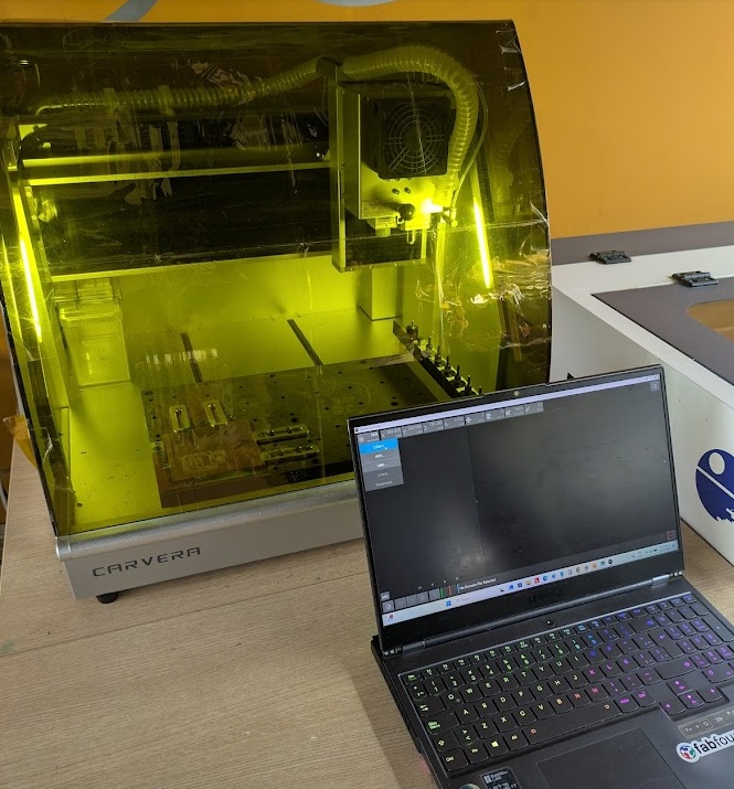
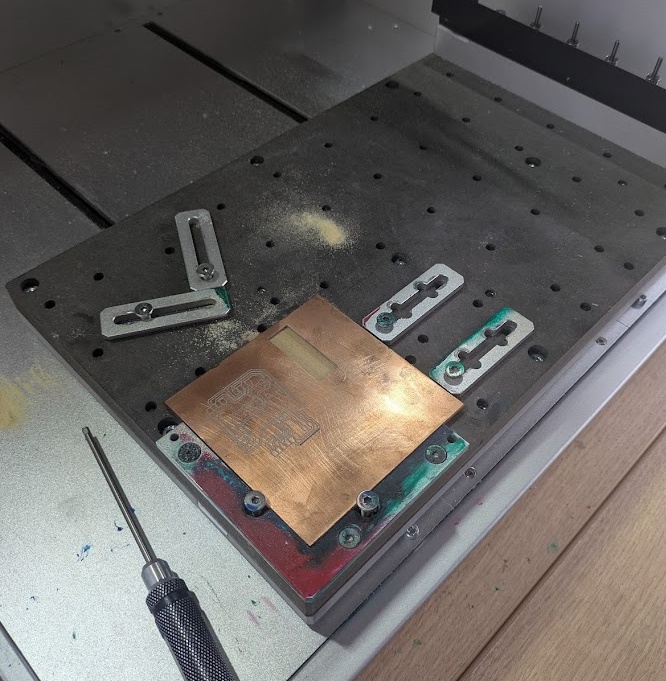
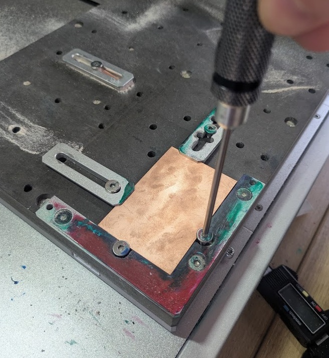
Once you're all set, connect to the machine by USB COM port, load your file into the onboard memory, select it, then provide it some settings for the job. We aligned the home axis 5mm away from the corner to accommodate for the screws holding the piece down. Always remember to measure the full size of your board before it goes in! One of my first mistakes was designing a board too wide for this little piece!
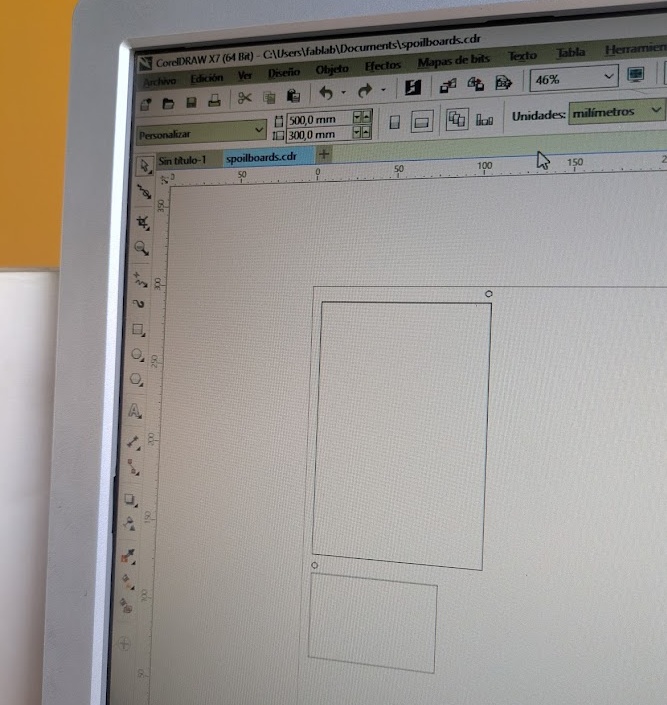
➔ Spoil Boards
We had three different sized FR1 stock at ESAN, but unfortunately for me I could only find one size of spoilboard, which is the substrate you put underneath the milling machine so the drill bit can pass all the way through the copper plate reliably, much like the CNC last week. Really, not a problem for me, because I get to go use my favourite machine again, the AVR-1400 laser cutter to cut out some more sized spoilboards.
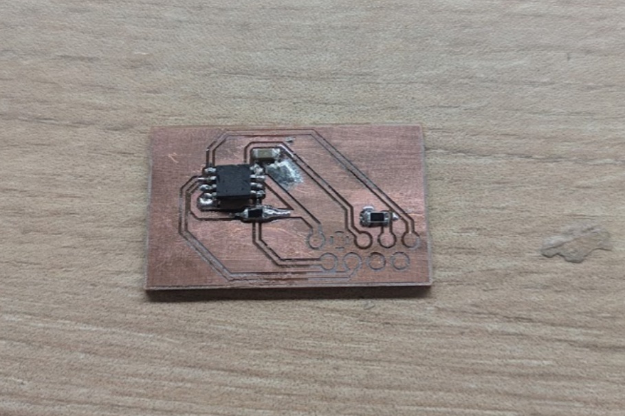
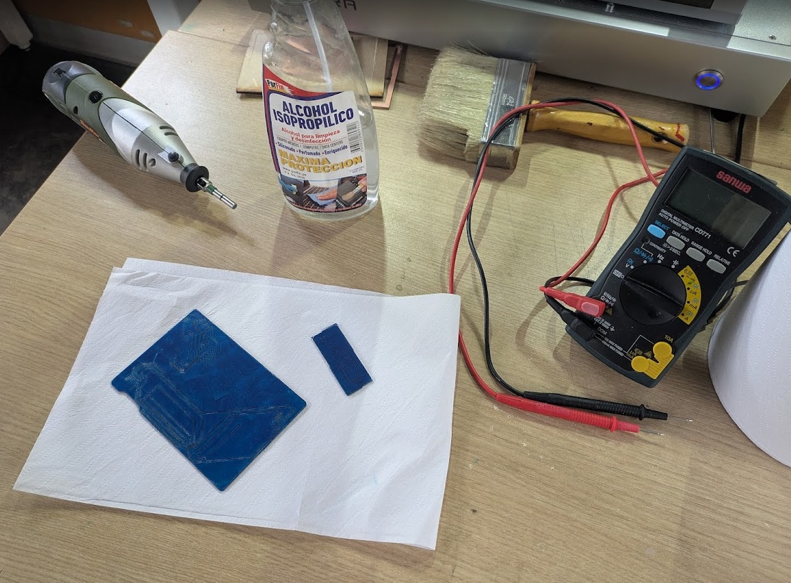
Soldering
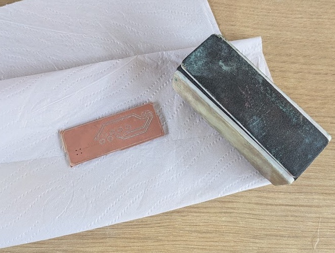
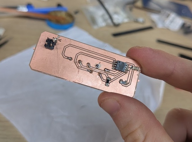
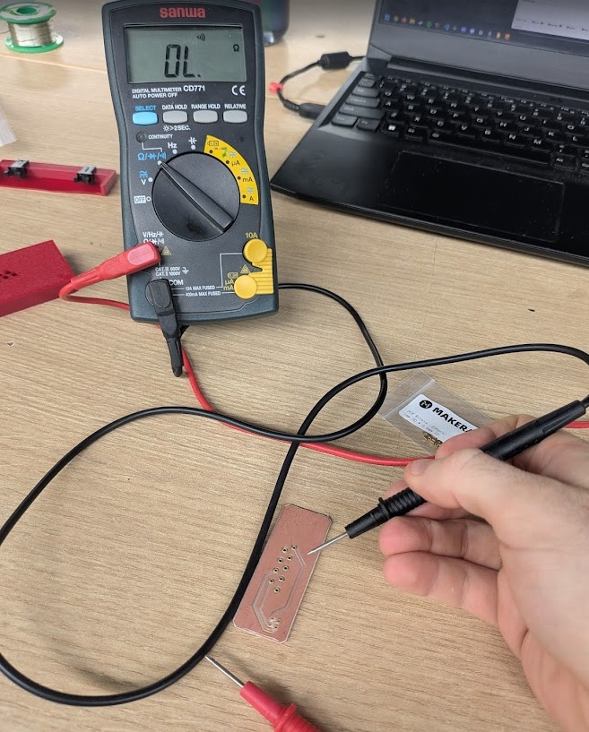
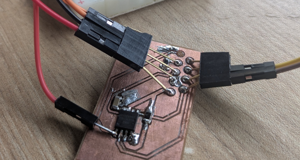
With your fresh PCB in hand, you're ready to start adding on all of the pretty components you designed it for! Before you start, give the board a quick little sanding again to remove any burrs or material that was roughed up by the mill. Also a good idea to test your traces with a multimeter for continuity.
This section I'm leaving intentionally a little sparse, because... well I've got lots to share about what NOT to do when it comes to soldering ahead.
Testing
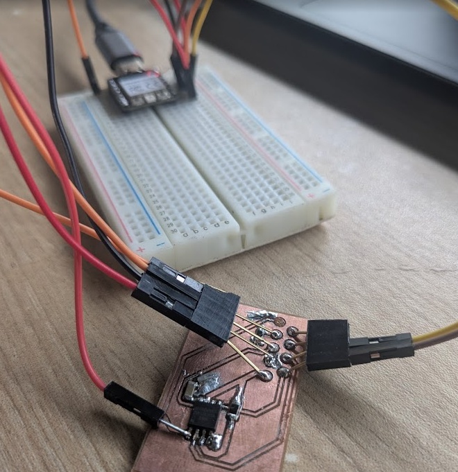
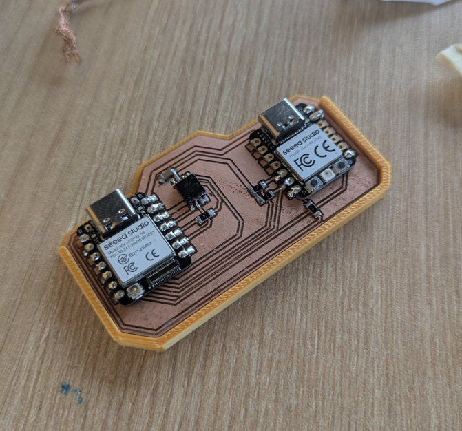
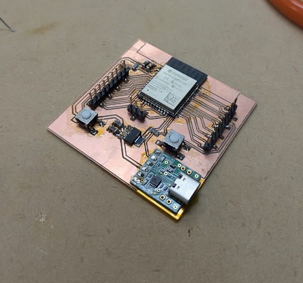
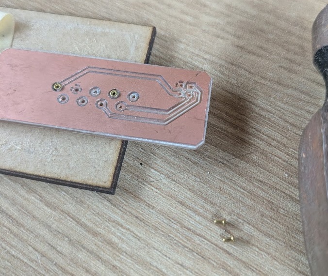
I managed to get all of the above finished and functional on my second try and on the first day of class! The circuit board I designed is the prototype for the cartridge PCB that holds the flash memory for my final project. I wrote a little python script to write a small chunk of data to the flash, and then read it back.
import board
import busio
import digitalio
import analogio
import time


spi = busio.SPI(board.SCK, board.MOSI, board.MISO)
cs = digitalio.DigitalInOut(board.D7)
cs.direction = digitalio.Direction.OUTPUT
cs.value = True
id_adc = analogio.AnalogIn(board.A0)

def read_jedec_id():
    while not spi.try_lock():
        pass

    try:
        spi.configure(baudrate=1000000, phase=0, polarity=0)
        cs.value = False

        # We send 4 bytes
        out_buf = bytearray([0x9F, 0x00, 0x00, 0x00])
        in_buf = bytearray(4)

        # sends and receives at the exact same time
        spi.write_readinto(out_buf, in_buf)

    return in_buf[1:4]

def read_cartridge_id():
    return id_adc.value

print("Hardware Test...")
time.sleep(1)

# Test 1: SPI Communication
print("/n Testing Flash Memory")
jedec = read_jedec_id()
print(f"Raw JEDEC Data: {[hex(b) for b in jedec]}")

if jedec == bytearray(b'\xef\x40\x18'):
    print("SUCCESS")
else:
    print("ERROR")

# Test 2: ID Resistor
print("\n Testing Cartridge ID")
raw_adc = read_cartridge_id()
voltage = (raw_adc / 65535) * 3.3
print(f" Raw Value: {raw_adc}")
print(f" Pin Voltage: {voltage:.2f}V")
And surprisingly, it worked on the first try (okay second try if you count me mixing up the MOSI and MISO lines momentarily).
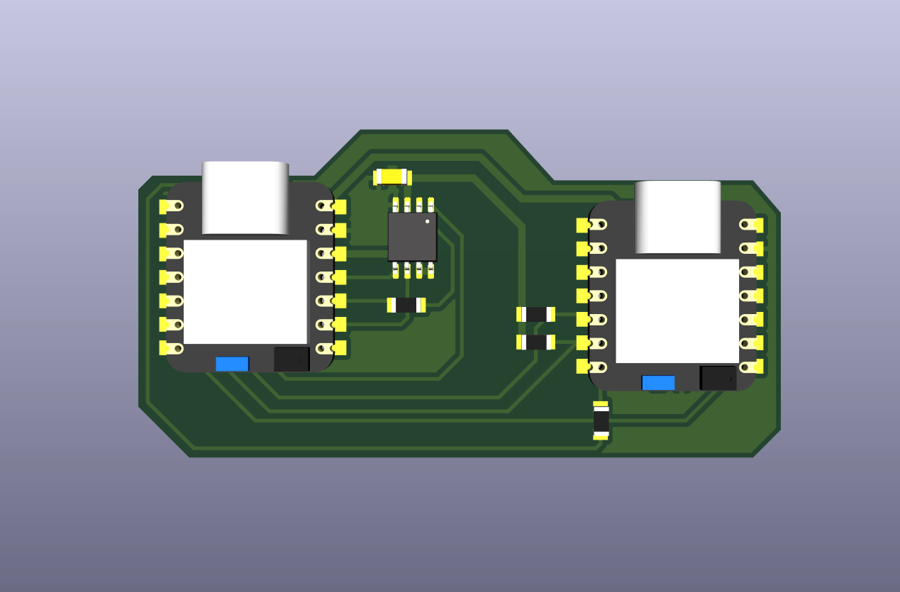
With my weekly assignment (at least a big chunk of it) underwraps in under 5 hours start to finish, I knew I would want to push myself to develop a deeper understanding of PCB development. After all, it's easily one of the top skills I joined Fab Academy for. My mentor, Jorge, challenged me to create a double-sided PCB, a PCB solder mask, and silk screen. I thought that this would be an excellent opporuntity to create a DEV KIT for my final project too, so I could start programming and testing on a more granular device, rather than having to worry about system integration in week 9. So... with my head held high with confidence, I got to work.
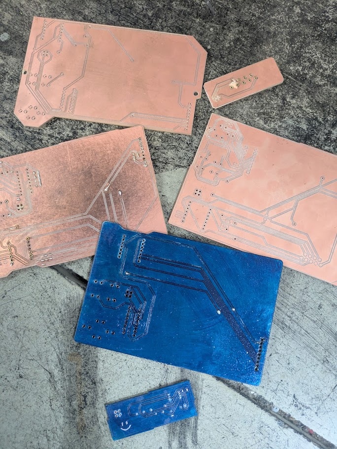
And... then I proceeded to have 4 days in a row of nothing but failure.
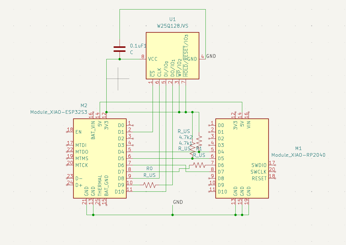
EDIT APRIL 23/2026: I believe I celebrated a bit too early in the above documentation. I technically did not in fact have the assignment underwraps. Completely missed the part where you need to have the microcontroller embedded in the board, not on a breadboard. And though I technically had a microcontroller embedded in the board designs I describe below, none of them ended up working in the end. I have since created several boards with a XIAO or an ESP embedded. Sharing a collection of photos to show the difference here. The big idea here is making sure you're correcting the right footprint in KiCAD, wether you're using TFT headers or SMD. I have examples of both below.
Failures
I constantly tell my students that failure is necessary and presents a great opportunity for data collection. Well, after six or seven ruined copper blanks, I am collecting a lot of data.
I didn't set out to manufacture a set of expensive, double-sided coasters for my PAK DevKit, but diagnosing this gauntlet of a process to create something that was more in line with a consumer grade product gave me exactly the kind of troubleshooting material the Fab Academy wants to see. Taking my own advice is brutal, but here we are. Let's review everything that went wrong.
➔ Machine Trouble
The Carvera isn't the worst machine to work with. Sure, I'm not in love with the software it ships with, but it does have automatic tool changing. The one thing I was not prepared for about this machine though, is how absolutely painstakingly slow it is. This wouldn't be that big of a problem if PCB manufacturing was more forgiving. This week, one misstep would set me back 2 hours of milling. It would take 45 minutes per side to engrave, and about 10 minutes per side to cut, with some extra time sprinkled in trying to get the piece mounted in place with tape and the dozen or so times that the Carvera just totally forgot what tool it had and started doing the wrong thing.
I will take a little bit of blame for not reading more before getting started, or not asking more questions when reaching that point where you have to start over, but it did feel like the whole workflow (gerber2png, modsproject and carvera controller) were trying to feed me lies throughout the whole week, and it was very time consuming to figure it all out.
➔ Solder Mask
I'm going to give you instructions for how to apply a solder mask, but I'm going to highly reccommend that you don't bother.
I really love being able to mill my own PCBs now, don't get me wrong. I think a PCB milling machine is necessary for a high quality Fab Lab so that you can quickly prototype and test circuits that need more than a breadboard. But that's kind of where the buck stops. You aren't really going to make beautiful high quality and consumer ready PCBs in the Fab Lab yourself, at least not without pulling your hair out, and even still, I'm going to say it's not really worth your time.
As a quick introduction: A solder mask is to ensure your freshly milled PCB, which is pretty much just bare copper save a few channels you've just cut out, does not short circuit or have any connections bridged unnecessarily by external metal components. This is especially helpful for double-sided boards which are just begging to be set down on a table with a stray bit or wire or metal loose.
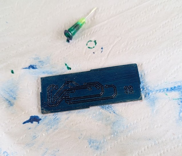
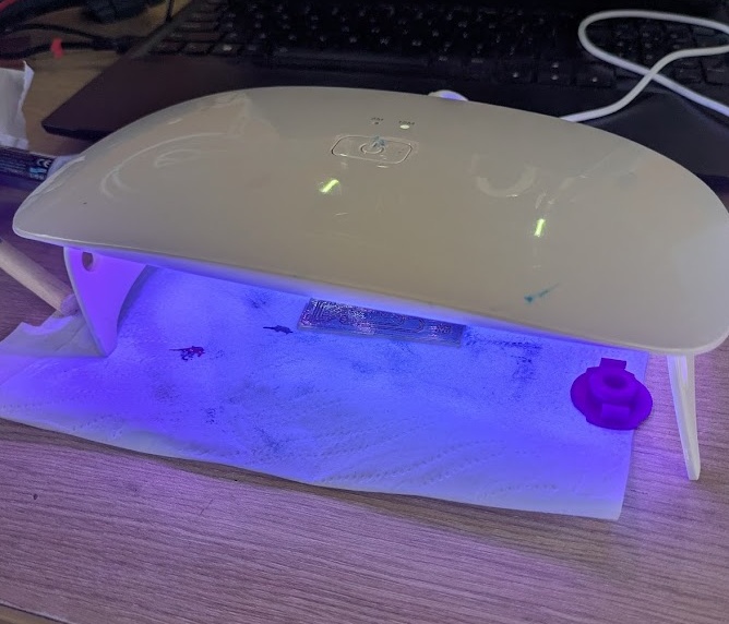
The mask comes in a liquid form (you'll want to wear gloves when handling, part of the reason you're not saying many in progress pictures here either), that you spread out thinly across your board with a roller or sponge, and then you let it cure using a UV light for 15 minutes. You'll want 2-3 coatings to ensure coverage. Aside from taking over an hour and a half (15 minutes * 3 coatings * 2 sides), it's a pretty simple thing right? Well, unfortunately by applying this mask, you've essentially just rendered your PCB unusable, as all of your solder points and... y'know reasons you milled the thing in the first place are now completely covered in a layer of insulation.
Normally, this is where you would ask your milling machine to lightly etch off all of the places on your board that you would need access to, you can even export a Gerber of this from KiCAD. However, it was at this point that I realized that my gerber2png and modsproject workflow had absolutely no setting to support this. I tried to bodge together a solution, manually creating a png file of all of the places I would need the mask removed, and then tricking modsproject into using a different toolhead and not digging as deep. But the problem now is that I have no (easy) way to tell the Carvera where the home is, and my whole frame of reference is gone.
So... I went about it manually. Handheld dremel in hand, I carefully stripped away a little bit of the UV mask (which I really did not apply evenly) from the PCB, exposing the copper underneath where it was needed.
This would all be well and dandy if it weren't for...
➔ Through Holes
This was absolutely one of my largest blindspots for this week. In my head, I'm thinking "you can just solder a throughole component to a board and it will always make the correct amount of contact with the copper on both sides!".
Hahahahahah.
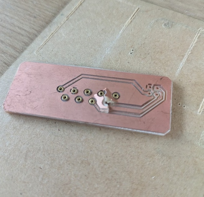
Not only were my copper pads completely covered in UV mask, they were also just 0.25mm thick in places. Not an easy job to scrap away by hand. Not to mention, you've got to be suuuuuper deliberate about soldering in such a way that allows the liquid solder to flow through to the other side of the board and make contact with both: your component and the trace on the other side of the board.
I was not good at this. So maybe I could come up with a fix? If I could expose a little bit of the copper, I could use one of the PCB rivets to connect the two halves and solder them together.
➔ Solder Pads
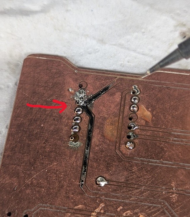
Which leads me to the many issues that arose trying to solder everything. Because the pads were so thin, they were also super delicate. Add a bit too much heat and press a little too hard (trying to desolder the component that you accidentally installed backwards) and welp, your copper is just GONE!
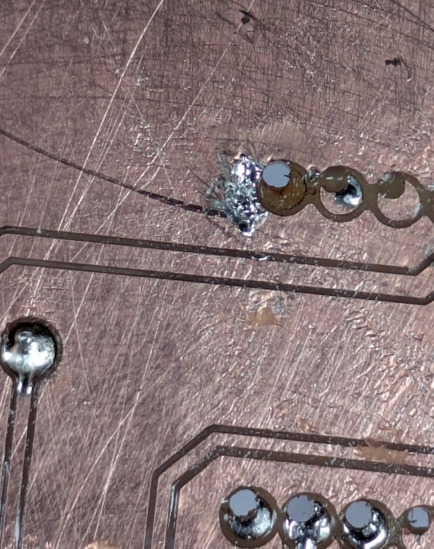
➔ Ground Plane
I've soldered lots of things before (though you probably wouldn't be able to tell based on the photos I've just shared with you), but I have never really soldered anything to a large ground plane before. To recap, to solder a joint, you want to heat it up with the tip of your iron, then introduce the solder to the joint (not the iron). The joint is hot enough that the solder melts and fills the joint. However, this doesn't happen as quickly when the joint you're trying to heat up has much more thermal capacity, as was such with the ground plane, which occupied most of the PCB. This is going to be super unforgiving if you make any mistakes.
And believe me, I made mistakes.
What did I learn?
- Read the f-ing manual
- Figure out if more than one thing went wrong if you're deciding to start over
- Inspect the outputs you get from your software BEFORE using them
- If you're going to do a solder mask, keep it in the machine
- Opt for surface mounted components where possible
- Don't rely on through hole connections for your PCB nets
- Don't push your iron too hot (under 375C is fine)
- Use a heat gun if you need to solder to the ground plane
- Use wider track sizes, increase annual diameter and increase the clearance between traces
and finally, if you want a pretty circuit board...
Just Buy it on PCBWay
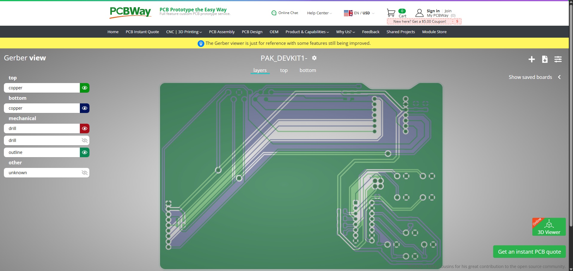
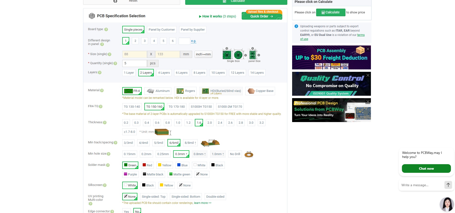
I've used PCBWay before to order some boards (not designed by me) for my students back in Toronto. PCBWay is a board house located in Guangdong, China that can produce your custom board in just a few short days and have it shipped out to you. All you need to do is select your board specifications, here I've chosen an FR4 board since there's no health risk associated if you're not milling it yourself. You can even get multilayer boards for super complex PCBs! You're also able to get the silkscreen done easily here (which I was unable to fully try out myself here at ESAN). You can upload your gerber files (similar to how we did it for gerber2png) and it will generate a preview.
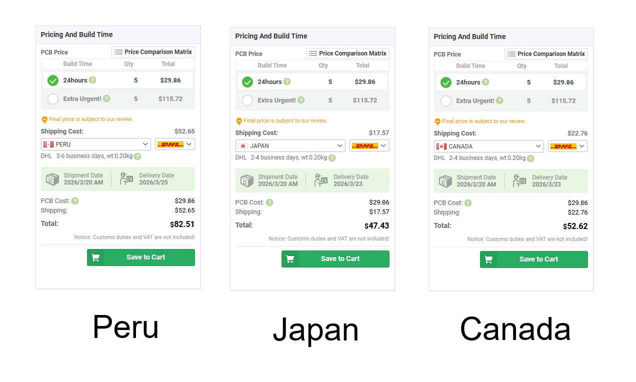
Oh, those shipping fees... Okay maybe I'll wait until I leave Peru.