INTRODUCTION
We move on to another critical aspect of electronics fabrication this week, something I have been itching to learn more about: how to design and fabricate printed circuit boards for custom projects. I've mentioned many times thus far that I'm a fan of breadboards - or a fan in the sense that they are kind of all I know short of dead bug circuits and alligator clips. I have ordered custom PCBs from PCBWay before, but never have I ever designed one myself. For this week, I designed the first iteration of the two PCBs needed for my final project, the PAK system and the PAK cartridges, as well running some more tests in a simulator for the software that will drive the display on the main system. You can also read about our group assignment at Fab Lab ESAN here.
[x] Use the test equipment in your lab to observe the operation of a microcontroller circuit board (as a minimum, you should demonstrate the use of a logic analyzer)
[x] Document your work on the group work page and reflect what you learned on your individual page
[x] Use an EDA tool to design a development board that uses parts from the inventory to interact and communicate with an embedded microcontroller
[x] Simulate a circuit

[ ] For my students:
Multimeters
Before applying full power or running code, a multimeter is the first line of defense to ensure the board won't short-circuit. Although my pomodoro timer circuit from week 4 already functions nicely, I did want to run some tests on it to demonstrate an understanding of how a multimeter can help troubleshoot circuits.
-
Continuity Testing: I used the multimeter in "continuity mode" (the beep setting) to check for bridges between the 3.3V and GND connections. This confirmed that my circuit and the breadboard was clean and that there were no accidental connections between power and ground.
-
Voltage Verification: Once I connected the XIAO RP2350 to USB power, I measured the voltage between the 3V3 pin and GND. I verified a steady output that hovered around 3.3V +/- 0.1V (as I am powering a current hungry screen), confirming that the onboard regulator was functioning correctly.
Simulation
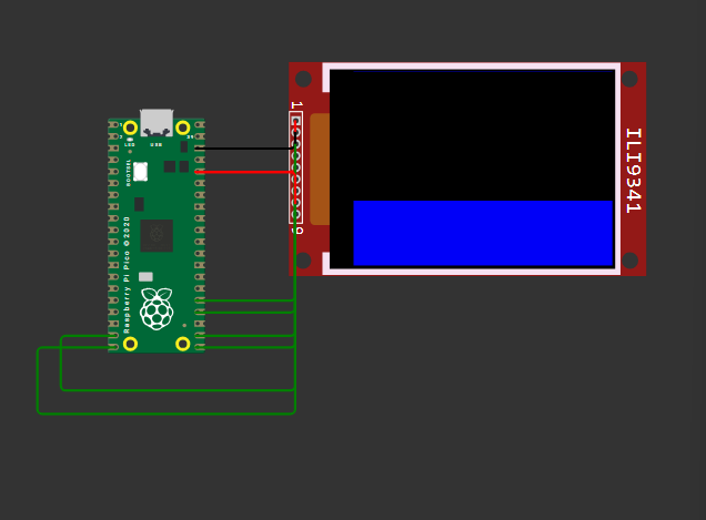
Before committing to any EDA and PCB routing for the PAK handheld device, I needed to validate the logic for the screen and directional inputs on the main device. Unfortunately, there isn't any simulation tool that would help me with my exact hardware, but Wokwi does offer a Raspberry Pi Pico (RP2040) environment with CircuitPython, which aside from some differences in clock instructions and pin numbers, would be functionally identical to the toolchain I'm using for the PAK. Wokwi doesn't have the exact display I ordered but it does have another SPI based TFT screen (ILI9341). I opted just to try out some simple I/O with a push-button D-PAD for this.
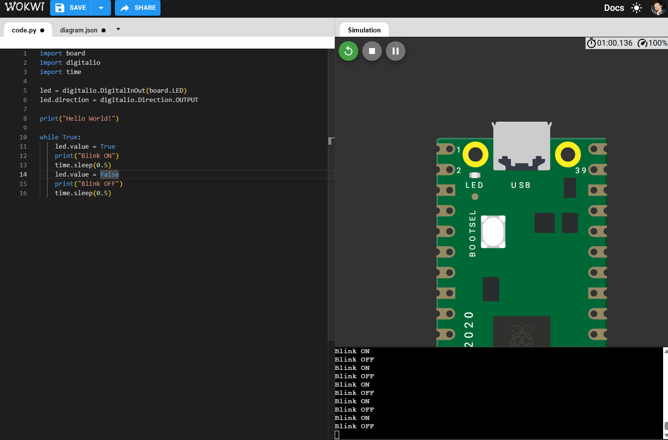
In Wokwi, you're able to import Adafruit bundle libraries just as you would on the XIAO, you just need to upload a requirements.txt file to the Wokwi workspace with the names of the libraries you want to reference. They are already part of the workspace, so no need to download anything. I uploaded a file with the following bundles referenced:
adafruit_ili9341
adafruit_display_text
My next step was to physically wire the components. I referenced the data sheet provided in the Wokwi documentation and tried to write some CircuitPython using the displayio library, similar to what I showed in week 04 with my final project.
➔ DISPLAYIO
The big idea to understand about this library is that displayio is that it does not draw pixels to the screen one by one in a continuous loop. Instead, it uses an object-oriented, layer-based hierarchy to build a scene in the microcontroller's RAM, and then intelligently updates the physical screen. I figured out a lot of this back in Week 04 but I was only playing with x/y coordinates. This time I was working with colour and sizing of objects using the Palette, Bitmap, TileGrid classes, creating objects with each and updating each instance in the while True loop.
import board
import busio
import displayio
import adafruit_ili9341
import time

print("hello")

displayio.release_displays()

try:
    spi = busio.SPI(clock=board.GP18, MOSI=board.GP19, MISO=board.GP16)
    tft_cs = board.GP17
    tft_dc = board.GP15
    tft_rst = board.GP14
except Exception as e:
    print(f"Error: {e}")

# set up display
display_bus = displayio.FourWire(spi, command=tft_dc, chip_select=tft_cs, reset=tft_rst)
display = adafruit_ili9341.ILI9341(display_bus, width=320, height=240)

#define screen
pixel_bitmap = displayio.Bitmap(display.width, display.height, 1)

#define palette
color_palette = displayio.Palette(1)
color_palette[0] = 0xFF0000 # Red

#tilegrid
screen_fill = displayio.TileGrid(pixel_bitmap, pixel_shader=color_palette)

#push to screen
main_group = displayio.Group()
main_group.append(screen_fill)
display.root_group = main_group

print("Red")

while True:
    time.sleep(1)
    color_palette[0] = 0x00FF00 # Green
    print("Green")

    time.sleep(1)
    color_palette[0] = 0x0000FF # Blue
    print("Blue")

➔ Push Buttons
My next step was to edit my code to allow the user to interact with the hardware through some push buttons. In my final design, I want to use a D-PAD and a few different face buttons to control the interface. A D-PAD typically isn't made with push buttons (they tend to use rubber domes with bridging contact pads for the best feel) but since that's not something that is easily simulate - and the goal here is to just register button pushes, I opted to try it out with just 4 push buttons instead. The code only needed a few updates:
# the 50x50 square
square_bitmap = displayio.Bitmap(50, 50, 1)
square_bitmap.fill(1)
square_tilegrid = displayio.TileGrid(square_bitmap, pixel_shader=color_palette, x=135, y=95)

# text in the center
text_area = label.Label(
    terminalio.FONT,
    text="PAK SYSTEM",
    color=0xFFFFFF,
    scale=2
)
text_area.x = 100
text_area.y = 120

# dpad setup (repeat these 3 lines for each button - left, right, down)
btn_up = digitalio.DigitalInOut(board.GP2)
btn_up.direction = digitalio.Direction.INPUT
btn_up.pull = digitalio.Pull.UP

while True:
    #repeat this section again for each button and intended behaviour
    if not btn_up.value:
        color_palette[0] = 0xFF0000 # Red
        square_tilegrid.x = 135
        square_tilegrid.y = 0
        print("UP Pressed: Square at Top Center")
        time.sleep(0.15) # debounce
A lot less debugging required here. Here's what it ended up looking like:
A Quick Note
In the real world, a microcontroller pin configured as an input is incredibly sensitive. If it isn't explicitly connected to a voltage source (VCC) or ground (GND), it is considered "floating." Exposed metal will pick up ambient electromagnetic noise which could cause the pin to flip back and forth between HIGH and LOW. In simulators, however, there is no ambient noise at all, defaulting to LOW if no electrical signal is passed through it. It's for this reason that you don't see any pull down resistors in the buttons above. The wiring function in Wokwi isn't the greatest either, so instead of clouding my whole simulation with extra wires and no breadboard to separate things, I opted to do the simulation sans pull-down and include this little note in my documentation. My PCB does have them!
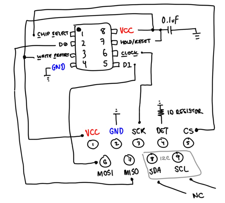
Schematic Design
To dip my toes in to KiCAD, I elected to try designing a simple cartridge for the PAK system first. I went through a few iterations of the drawing based on what I read in the datasheet for the flash memory chip I'm using, and I revisited the cartridge again once I had the PCB layout completed. It's a spiral process!
Here's how I got the first simple version of the board completed (and how you can too!):
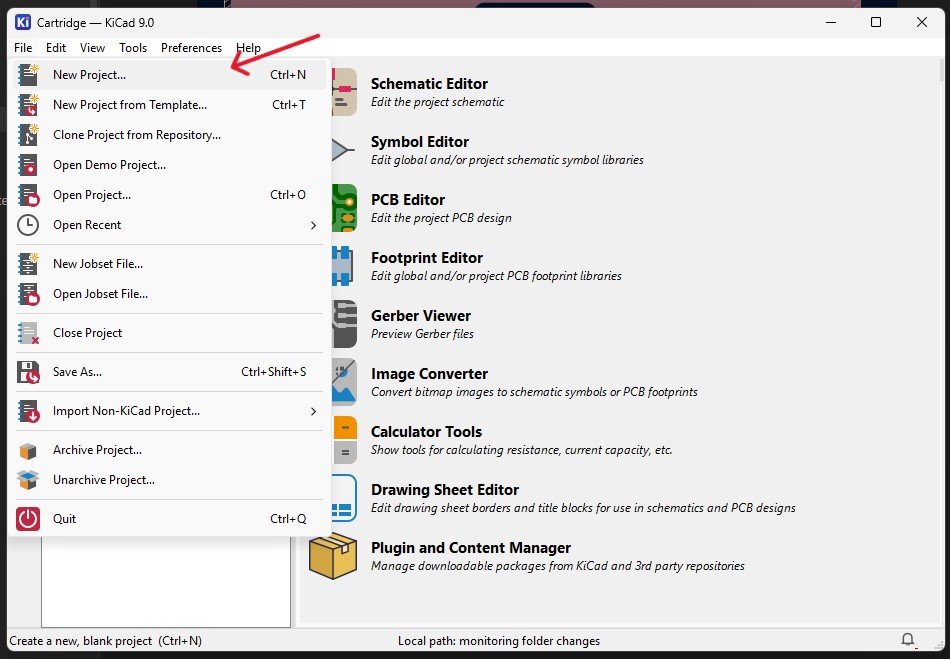
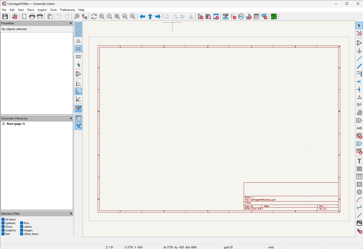
- Step 1: Start up KiCAD and click on File > New Project or Ctrl+N. Give your project a name. This will create two new files, a .kicad_sch and a .kicad_pcb file. The schematic and the circuit board.
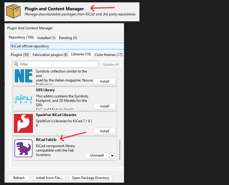
- Step 1b: (For Fab Academy) Before starting, quickly import the FabLib Library of components (found in most of the fab labs). Click on "Plugin and Content Manager" > Libraries tab > scroll all the way to the bottom > Install KiCad FabLib.
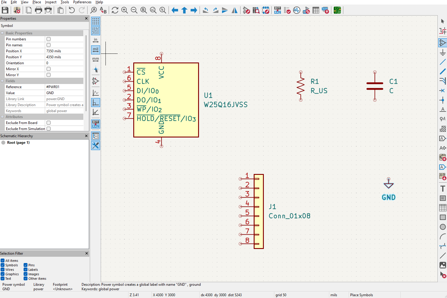
- Step 2: Click on the schematic editor. This will open a new window. Here:
- Pressing "A" will let you "Add a Symbol" or place a component on the schematic.
- Search for your components by name and place them anywhere on the schematic.
- In my case, I'm using a
W25Q16,Resistor,Capacitor,GND, andConn_01x08
- Step 3: On your keyboard, tap "W" to use the wire tool. Connect your wires as per the needs of your schematic.
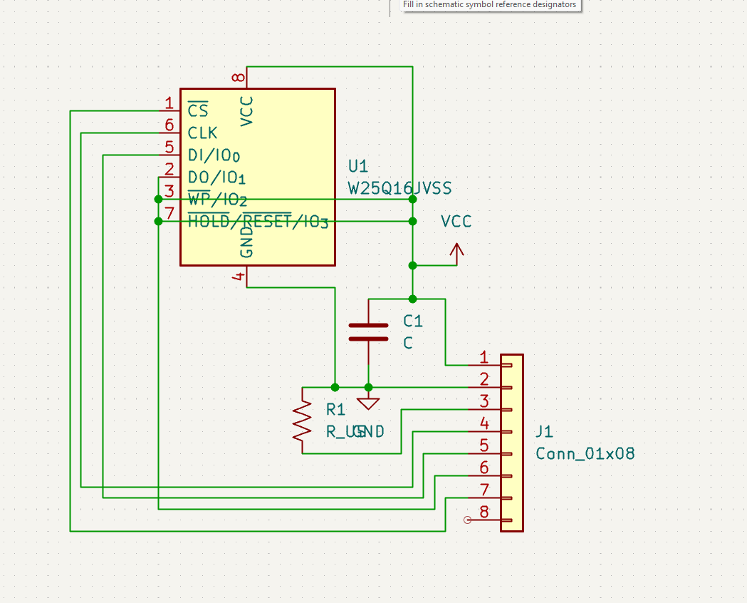
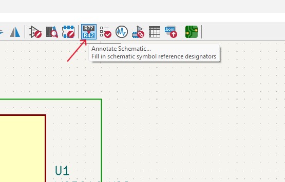
- Step 4: Check the schematic.
- Run the "Fill in schematic symbol reference designators" (This will annotate any of the capacitors and resistors used)
- Run the "Electrical Rules Check" (This will tell you if anything is disconnected)
- Run the Footprint Assignment (This will allow you to select the actual surface mounted components that you'll be using on the PCB for the generic items you may have selected)
- Step 5: Save your work and then switch to the PCB Editor with the green symbol on the right side of the menu bar.
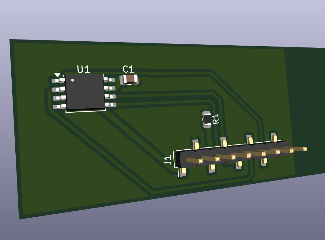
PCB Design
KiCAD asks you to configure your work in two stages, draw a schematic first to get all of the circuit logic sound, then translate it to a real "footprint" that removes the layer of abstraction that the symbols provide, asking you to place the physical components on a board, and how they'll be connected with traces (not wires), that will ultimately get machined. Continuing with our tutorial from above:
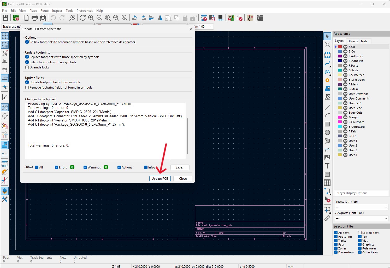
- Step 6: In the PCB Editor, press F8 to import/update components from the schematic file. When you click "Update PCB", just place all of your components somewhere in the center.
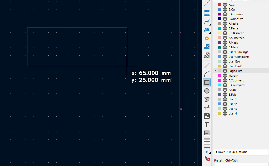
- Step 7: Select the "Edge.Cuts" layer in the right hand appearance menu and then the rectangle tool. Draw out the dimensions of your board.
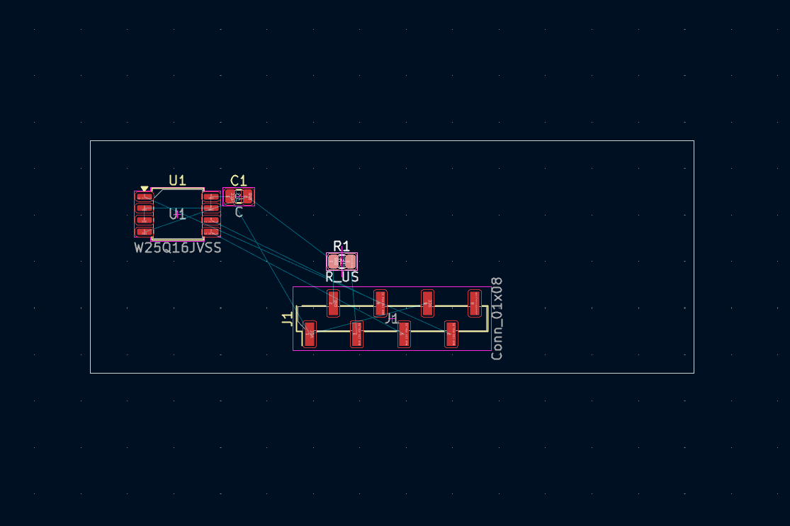
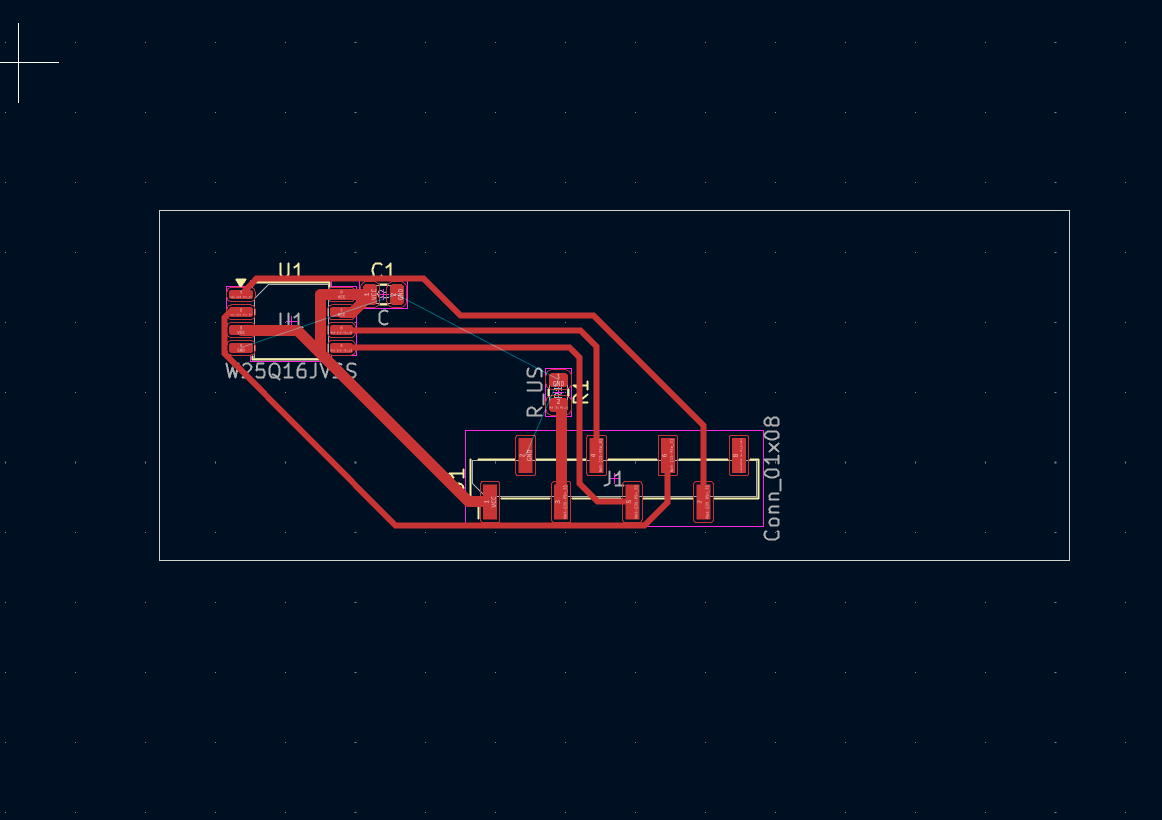
- Step 8: Place your components where you want them to appear on your board
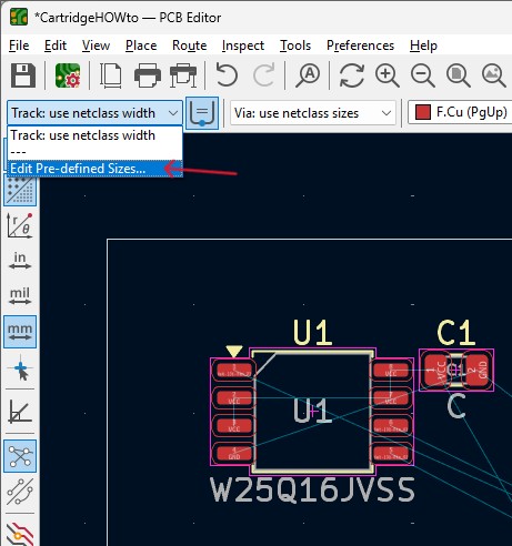
- Step 9: Define the width of your traces that you will use in the upper left, click "Edit Pre-defined sizes..." and add new tracks. In this case I am using 0.8mm traces for any power lines and 0.4mm thick traces for data lines.
- Step 10: Place your traces as per your needs. This takes some practice. Do not place traces for your GND connections. In my case, I read online that it's a good idea to route your Clock first so that it has the shortest trace to minimize interference. Also, depending on your machine, you may need to open up File > Board Setup... to manually enter a minimum clearance for the toolhead's thickness.
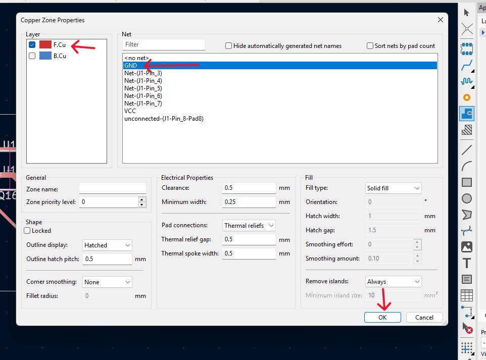
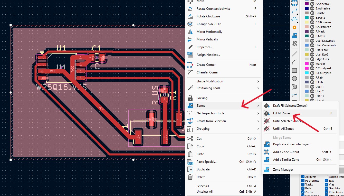
- Step 11: To add a ground plane, click on the "Add Filled Zones" tool on the left, and importantly, just click once (don't drag a box) where you want your ground plane to begin.
- Step 12: You can view your PCB in 3D by clicking Alt+3 or the 3D Viewer
As always I encourage you to check out the specific progress I've made on my final project as it pertains to the current week's topic, over on my dedicated final project page.

Conclusion
Week 6 was a massive leap from the world of breadboards (which was really all I knew prior to this week) into actual professional EDA workflows. Moving the PAK system from conceptual wiring to a fully routed, double-sided PCB felt like the first real step toward a finished product rather than just a collection of parts. It was a little frustrating working with Wokwi, to be honest. I don't think the simulations available right now are capable of running the code that I want to push myself to learn. I have personally reviewed and taught a lot of existing TinkerCAD and Microbit simulations, so it felt a bit like the part of the assignment this week that asked us to simulate was not able to meet me at my skill set.
The real learning curve was in the physical constraints. If I were to do this over, I’d probably skip the generic connector symbols and build custom footprints for the XIAO and display from the jump to save time on the back end. I think taking the time to create custom footprints is a skill I should be practicing, seeing as it looks like the KiCAD community doesn't have a lot of footprints available on the web - not sure I'm looking in the right places though. I'm excited to work on the actual fabrication of this board in 2 weeks!