During this week, we learned the complete workflow for electronic production, from generating manufacturing files to milling, soldering, programming, and testing an electronic board. This process allowed us to understand digital fabrication techniques applied to PCB production and microcontroller programming.
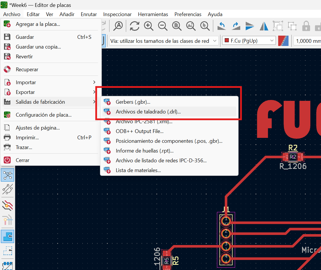
Using the electronic board designed during the electronic design week, we proceeded to fabricate the PCB. For this process, we exported and saved both the trace files and the drill hole files.
Figure 1. Exporting trace and drill files
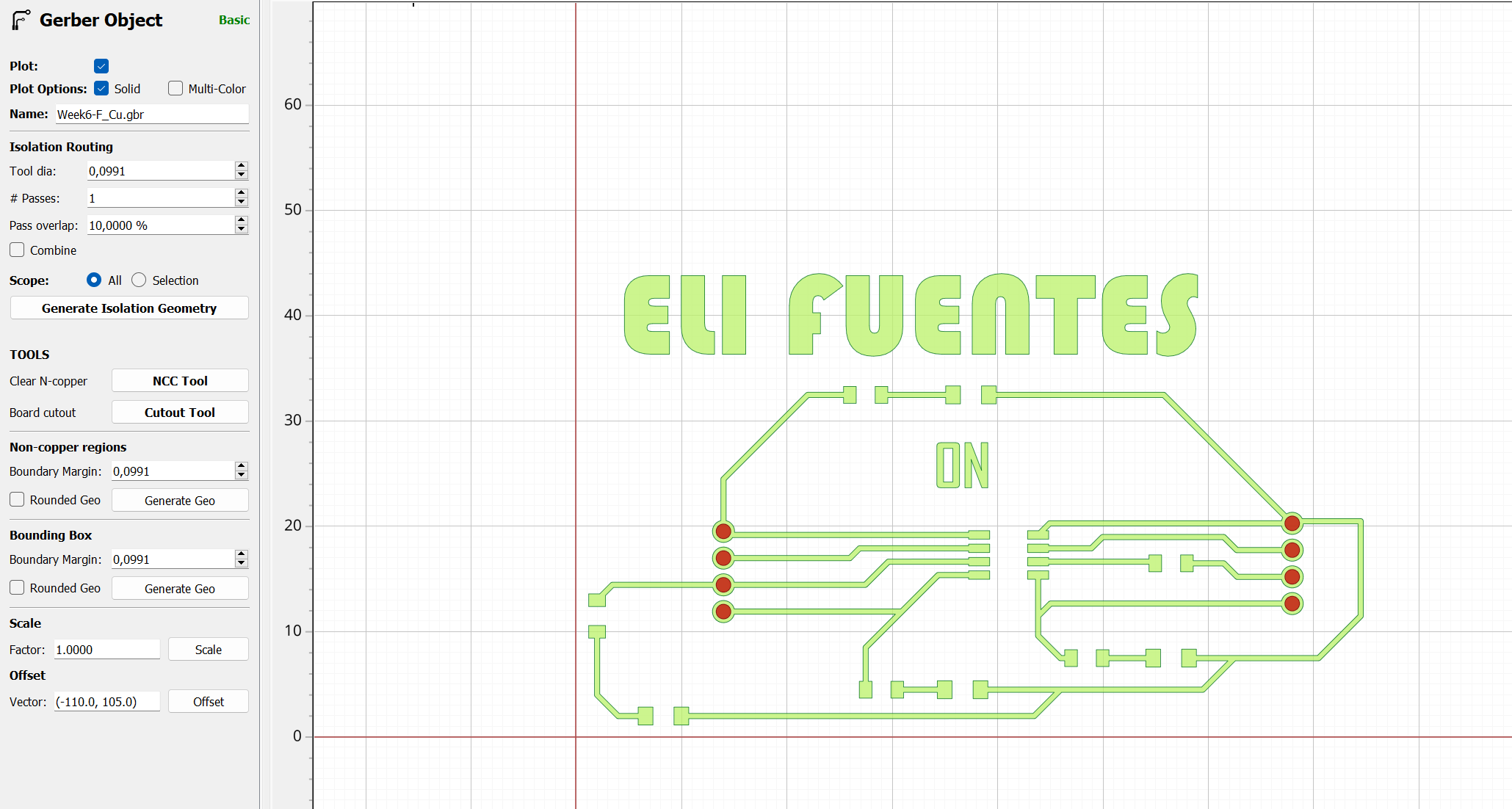
We started the FlatCAM software and imported the Gerber files for the traces and the Excellon files for the drill holes. Then, we positioned the design close to the coordinate origin point.
Figure 2. Importing Gerber and Excellon files in FlatCAM
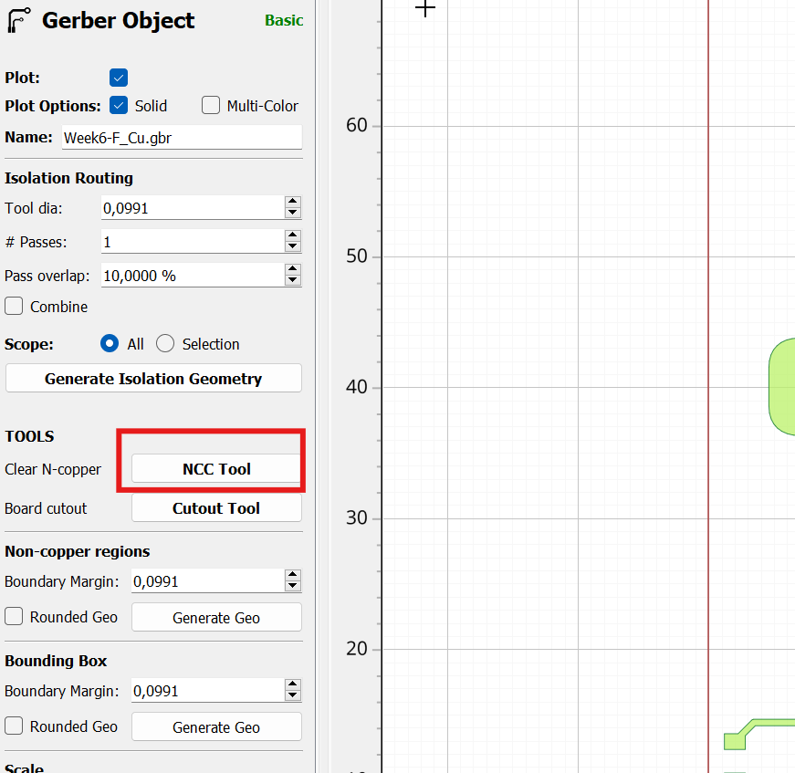
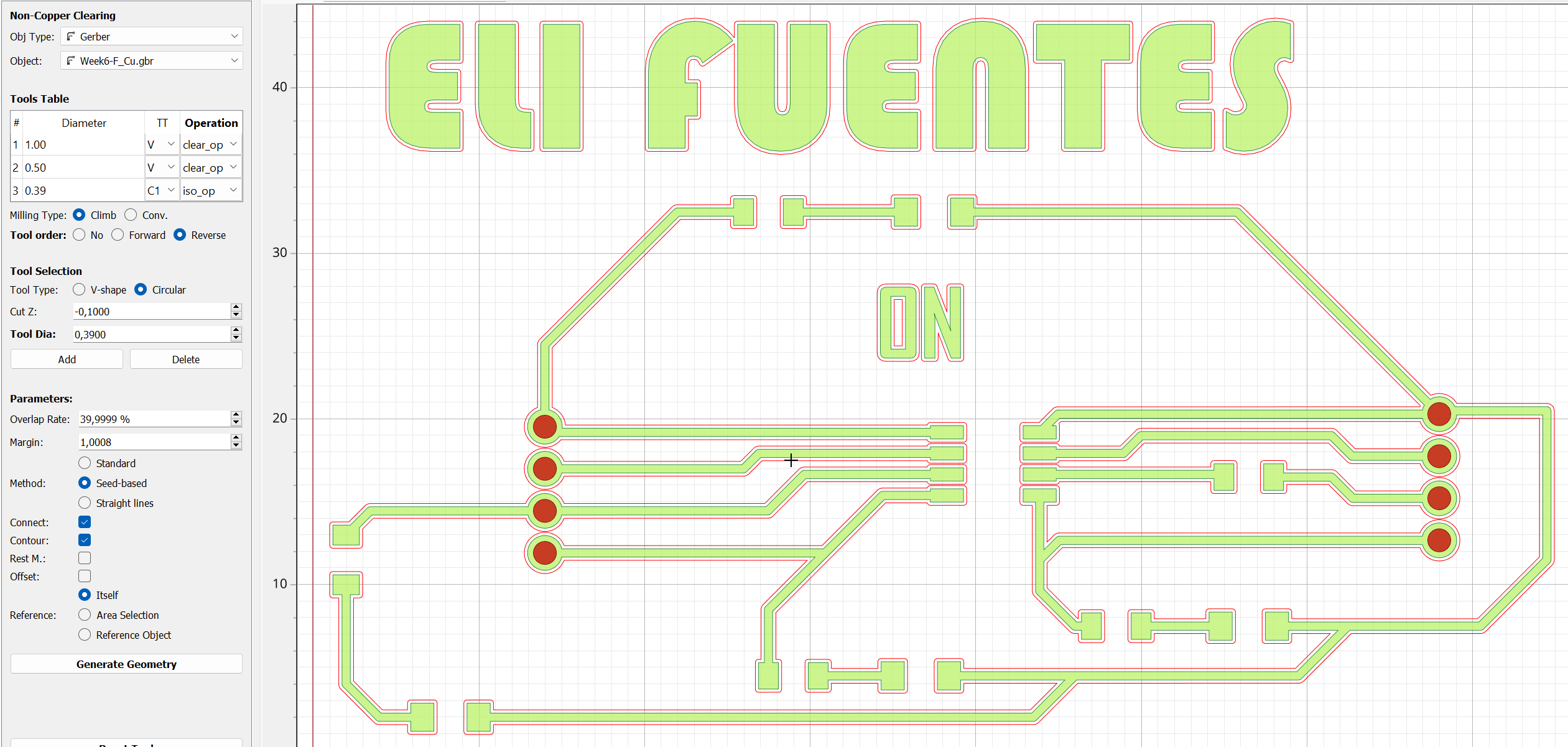
First, we generated the G-code for the PCB traces by configuring the tool through the NCC Tool option.
Figure 3. Generating G-code for PCB traces
We configured the milling parameters and selected the tool to be used. In this case, we used a 1/64” end mill with a machining depth of 0.1 mm on the Z-axis. Then, we generated the geometry, which displayed the toolpath in red lines.
Figure 4. Toolpath generation for PCB traces
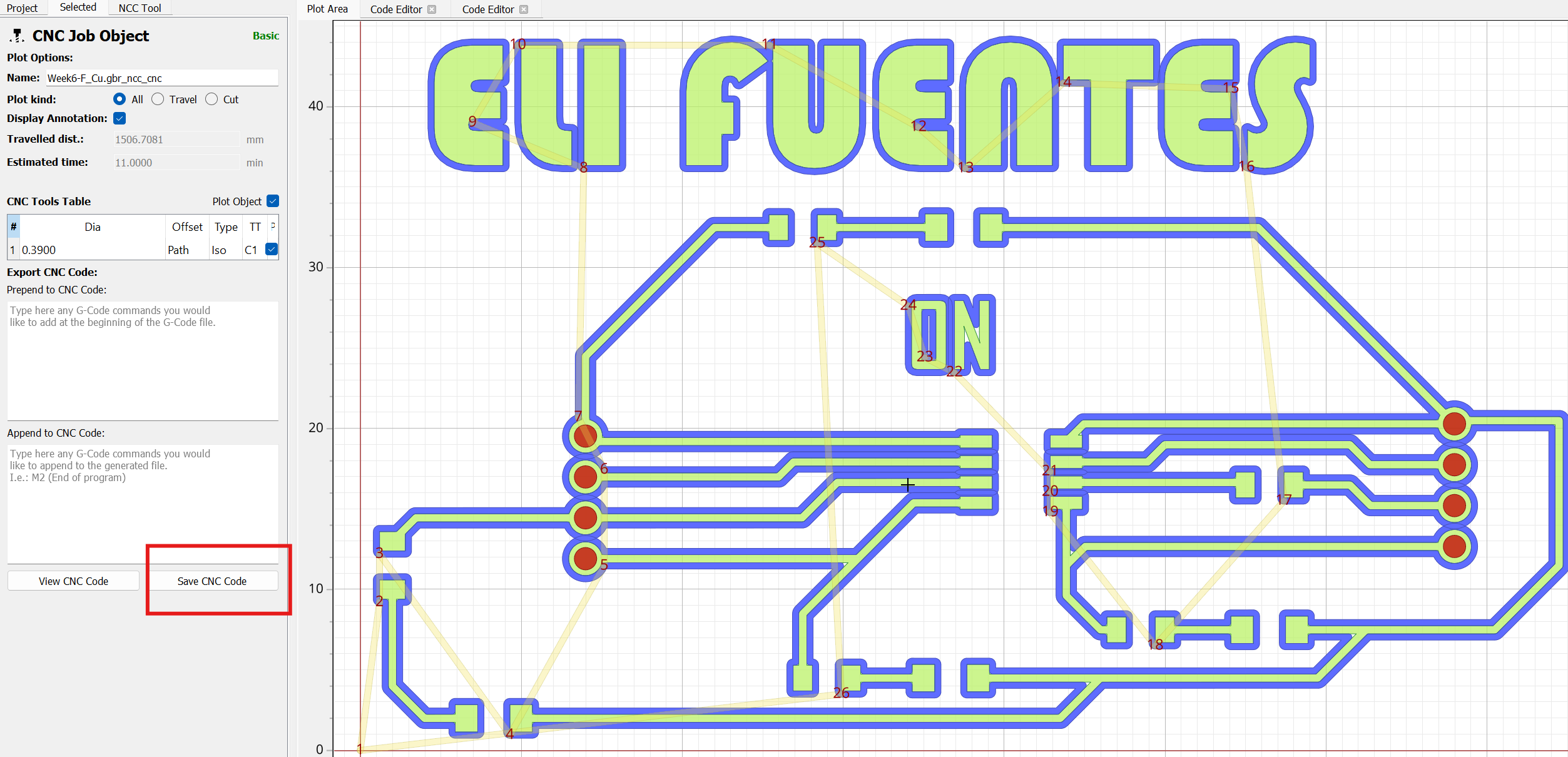
After configuring the parameters, we generated and saved the G-code for the electronic traces.
Figure 5. Saving the PCB trace G-code
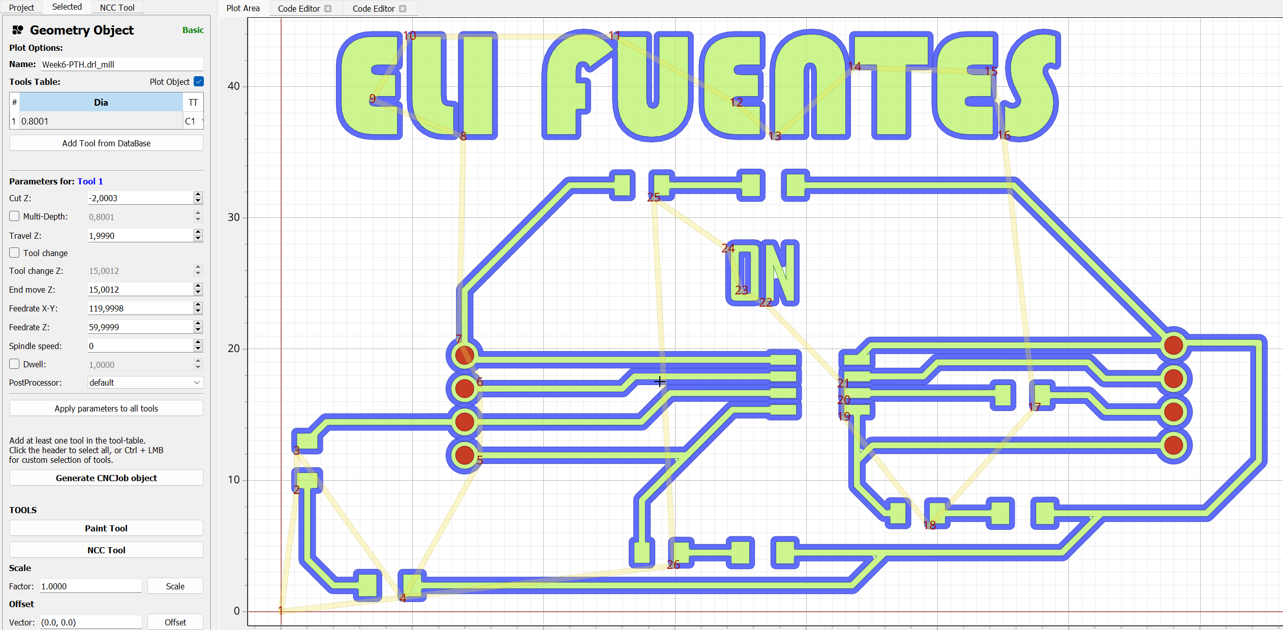
Next, we configured the tool for drilling the holes using a 1/32” end mill. We generated and saved the corresponding G-code.
Figure 6. Generating G-code for PCB drilling
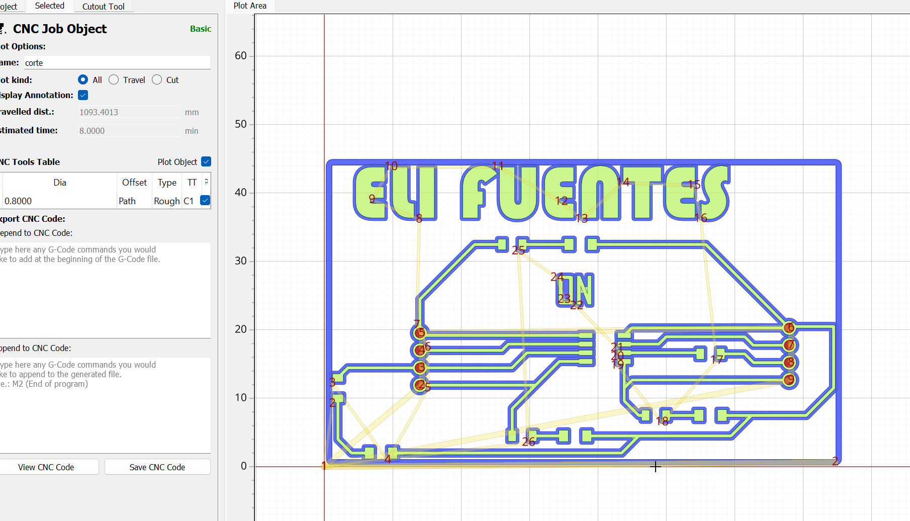
Finally, we generated the board outline to cut only the required section of the PCB.
Figure 7. PCB outline generation
Than the copper board is placed on the milling machine, ensuring the material dimensions were sufficient for the machining process. In this case, we required an area of 8 × 5 cm.Later on, We connected the Roland SRM-20 milling machine to the computer and powered it on. Then, we opened the software used to control the machine.
Figure 9. Connecting the SRM-20 milling machine
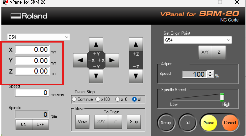
We set the machine origin according to the copper board position.
Figure 10. Setting the machine origin
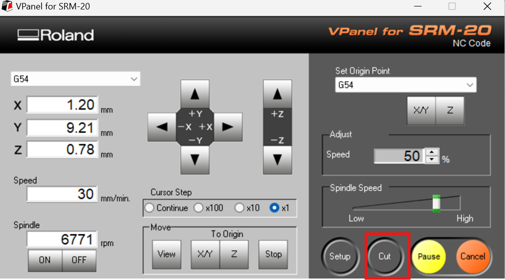
We adjusted the machining speeds, selected the corresponding G-code file, and started the milling process.
Figure 11. PCB milling process
We verified that the milling process was performed correctly. It was necessary to change the milling bit when machining the drill holes and the board outline.
Video 12. PCB milling verification process
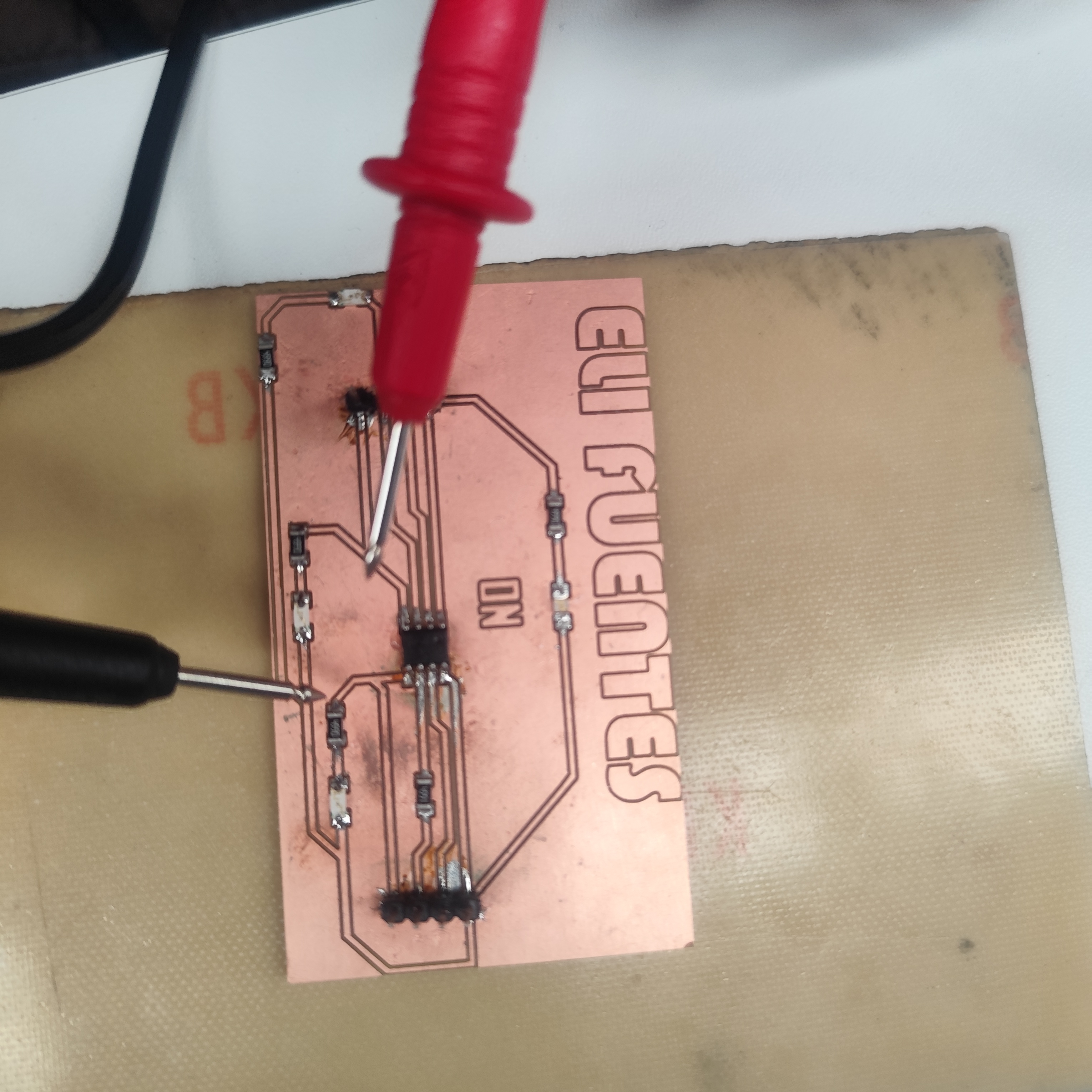
We checked that all traces were correctly fabricated using a multimeter to verify that there was no unwanted continuity between traces. Then, we soldered all electronic components and verified their correct positioning using the multimeter.
Figure 13. Soldering and continuity testing
In the Arduino IDE, under File → Preferences → Boards Manager URLs, we added the following link:
http://drazzy.com/package_drazzy.com_index.json
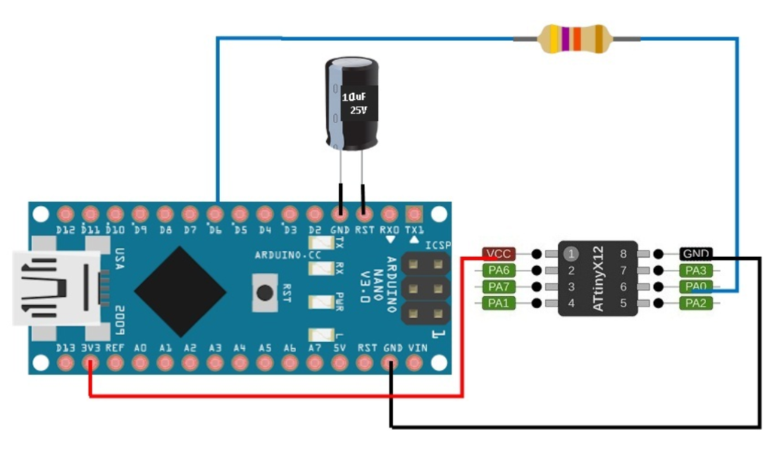
This allowed us to install additional board packages. Then, we installed the megaTinyCore library. After that, we uploaded the jtag2updi code from the GitHub repository to the Arduino Nano. Finally, we connected our PCB to the Arduino in order to upload programs to the board.
Figure 14. Programming setup using Arduino IDE
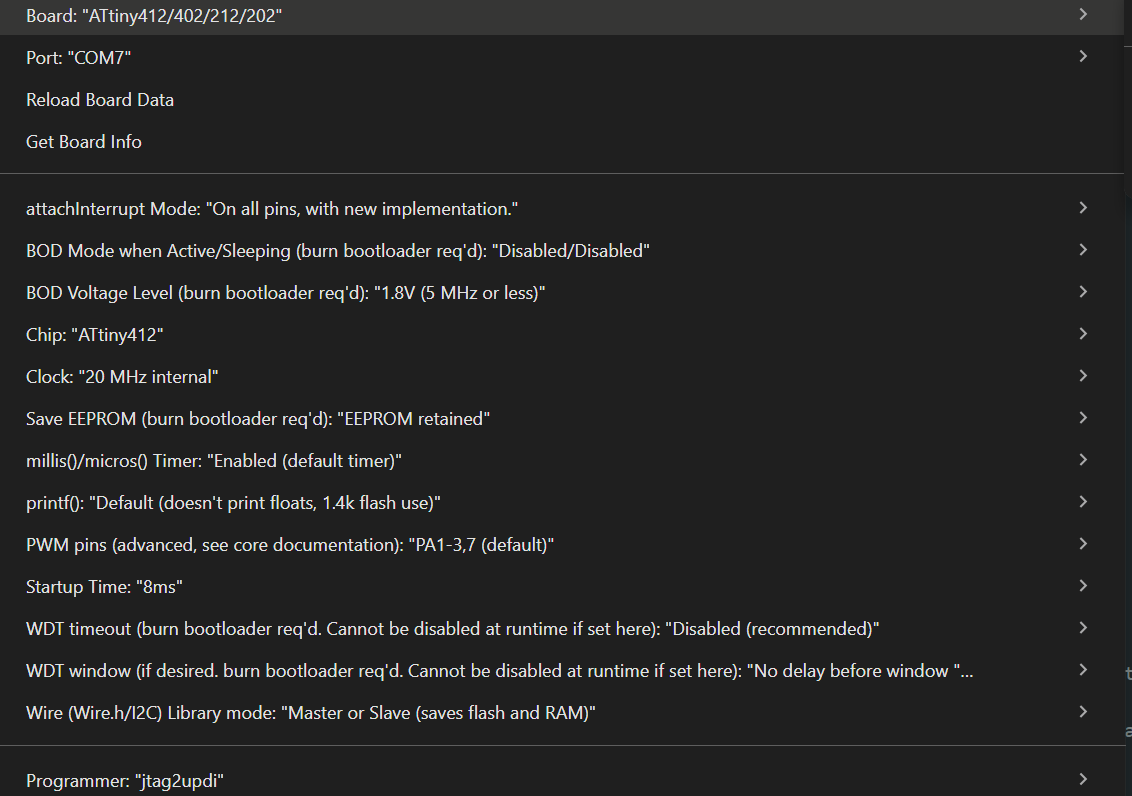
We wrote our program and ensured that the correct board and configuration settings were selected before uploading the code.
Figure 15. Uploading the program to the PCB
Finally, we uploaded the program to the board and verified that it functioned correctly.
Video 16. Final functional test of the PCB
Results
As a result, we successfully fabricated, soldered, programmed, and tested our electronic board. We learned how to prepare manufacturing files, generate G-code, operate the SRM-20 milling machine, solder electronic components, and upload programs using Arduino IDE and UPDI programming methods.
Conclusions
This week was particularly challenging because electronics production is outside our main academic background as architecture students. Understanding PCB fabrication, electronic components, programming workflows, and machine calibration required developing completely new technical skills. However, this experience allowed us to expand our knowledge beyond architecture and understand how digital fabrication and electronics can be integrated into interdisciplinary design processes.