
Week 08: Electronics Production
Assignments:
Group Assignment
- Characterize the design rules for your in-house PCB production process
- Submit a PCB design to a board house
- Document your work to the group work page and reflect on your individual page what you learned
Individual Assignment
- Make and test an embedded microcontroller system that you designed
Things to Complete This Week
- Re-design Final Project PCB with updated components
- Document design process of the object
- Learn how to use the CNC machine
- Include design files!
Here is my schedule for this week.
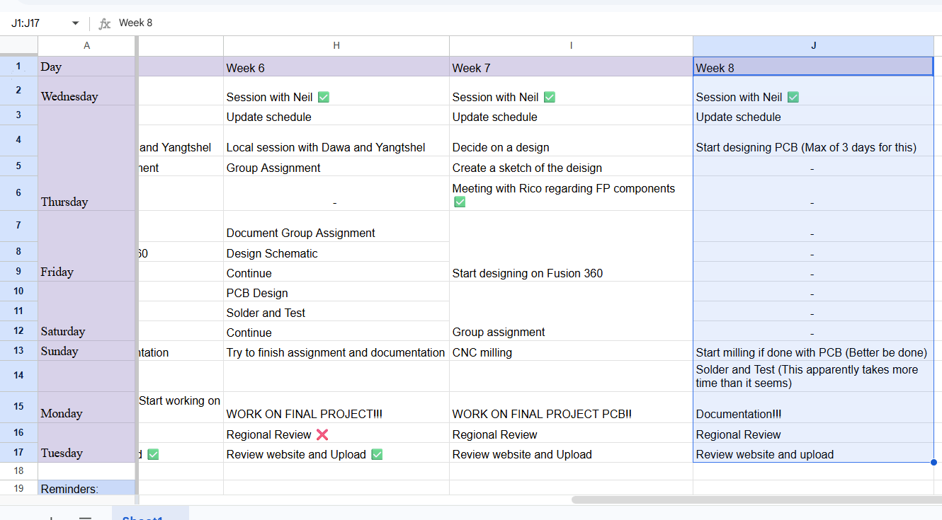
Here is the link to my schedule
Group Assignment
You can access our group assignment here.
Individual Assignment
I started this week by re-designing my Final Project's PCB 😮💨. Based on feedback (From Sir Rico and Sir Anith) and research, I’ve made these three changes:
1. Reducing pin usage
Connect all ultrasonic "Trigger" pins to a single pin on the microcontroller. This reduces the number of pins used - YAYYY! 😄.
2. Signal-Based Navigation
I’ve decided to move away from the whole "camera tracking a specific colour marker" and am planning to implement a Bluetooth following system 💙. I want to design a small wearable device that will continuously send Bluetooth signals so that the backpack can follow that signal. I feel like this will be more reliable than the camera, because in the camera's case, I'd have to consider a lot of other factors like lighting.
3. Microcontroller
To support these new changes and keep the project realistic, I am switching to the XIAO ESP32-C3 😁
XIAO ESP32-C3
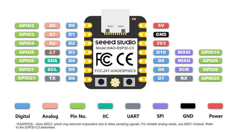
The XIAO ESP32-C3 will read distance data from three HC-SR04 Ultrasonic Sensor modules placed at the front, left, and right to detect obstacles. I will also use the built-in Bluetooth on the C3 to communicate with a small device carried by the user, allowing the backpack to follow the Bluetooth signal.
The backpack will move using two DC gear motors controlled by a TB6612FNG motor driver. By changing the motor directions, the backpack can move forward, reverse, or turn. The motor speed is controlled using PWM from one GPIO pin.
I will also connect a DFPlayer Mini MP3 Module through UART so the backpack can play audio from a microSD card through a small speaker. Since all nine usable GPIO pins on the C3 are used, there are no spare pins left.
Designing the PCB
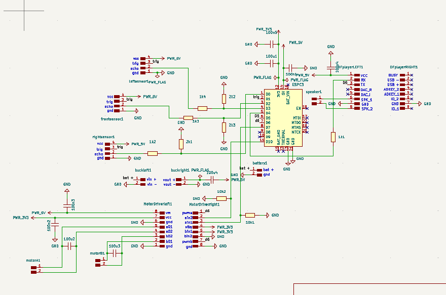
Note: I have not included the full steps of designing a PCB on this page. You can view the full process in my week 6 (Electronics Design) page.I first started with the schematic design. I ran the Electrical Rules Checker and came across a few errors. Most of them were because I had not assigned footprints to the symbols, and the others indicated that an input pin was not being driven by any output pin.
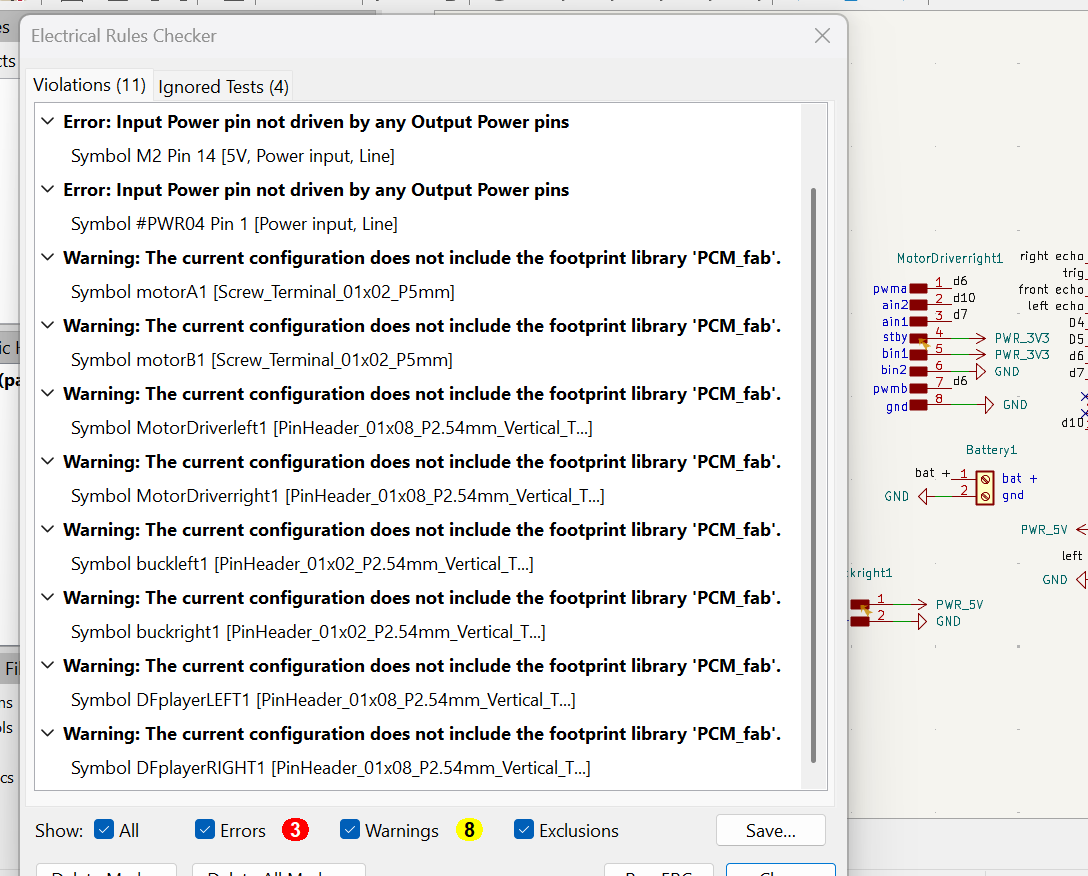
To resolve this issue, I added power flags to indicate that the nets were being powered.
What is a power flag?
A Power Flag is a small marker you add in a PCB schematic (like in KiCad) to tell the software that a wire really has power on it.
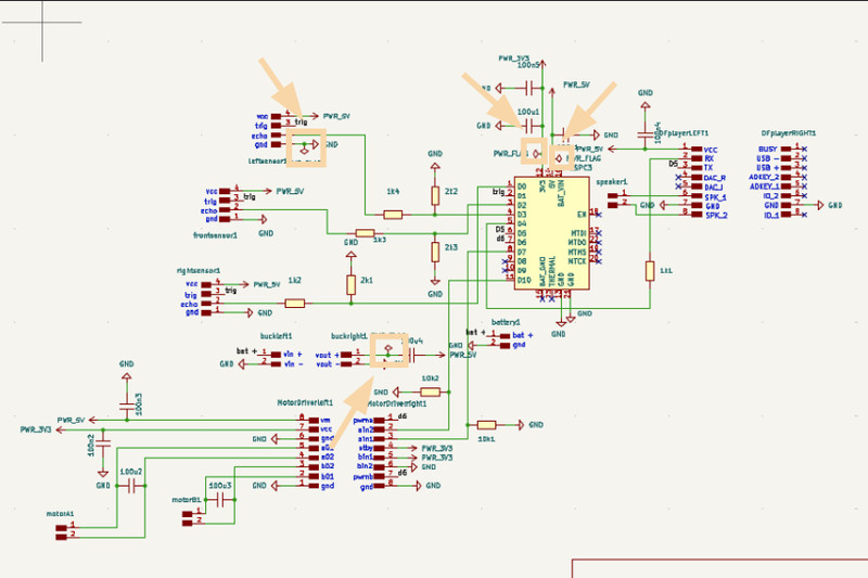
Here is the complete design with no errors 😁:
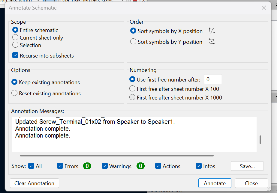
After completing the schematic design, I annotated it. Annotation assigns reference numbers (such as R1, C1, and U1) to the components so they can be properly identified in the PCB layout.
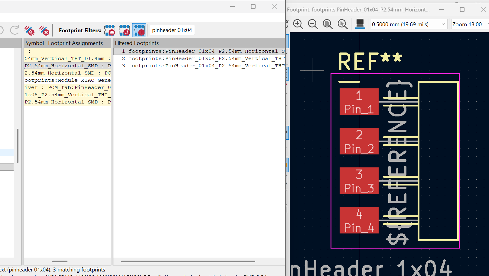
I then started assigning footprints to the components.
Now for the routing part. These were all the components that I had to route.
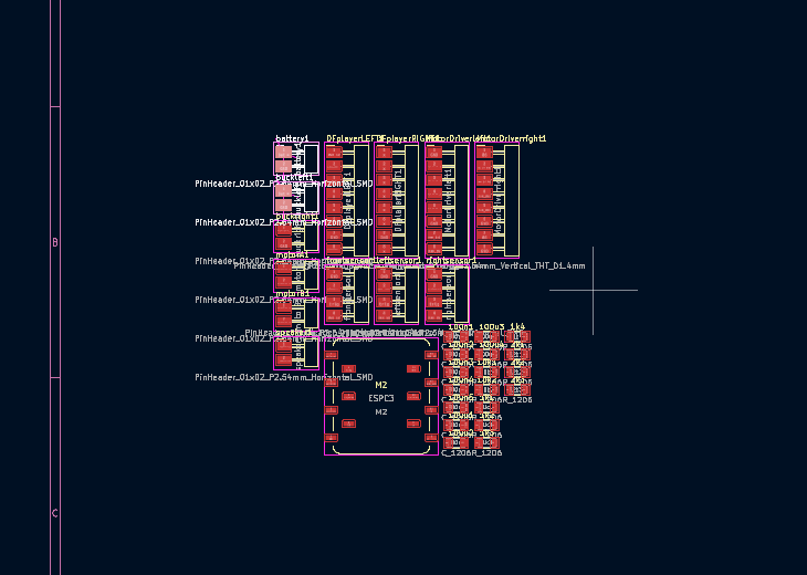
This was my first attempt, and it was nowhere near ready for routing. 🥲
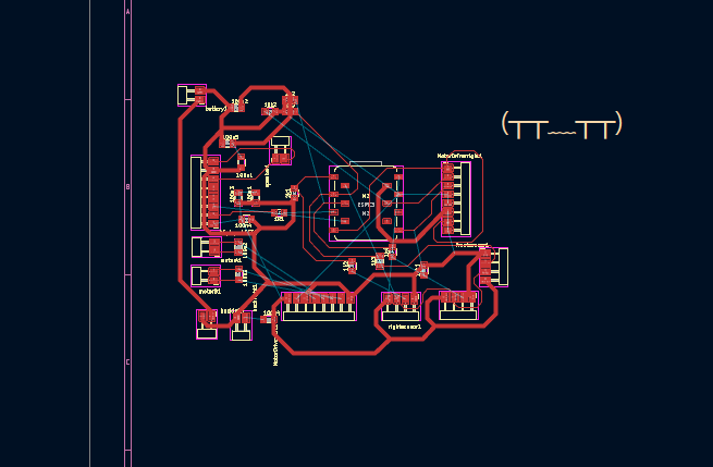
My second try turned out much better than the first, and I thought it might just work. 🤔
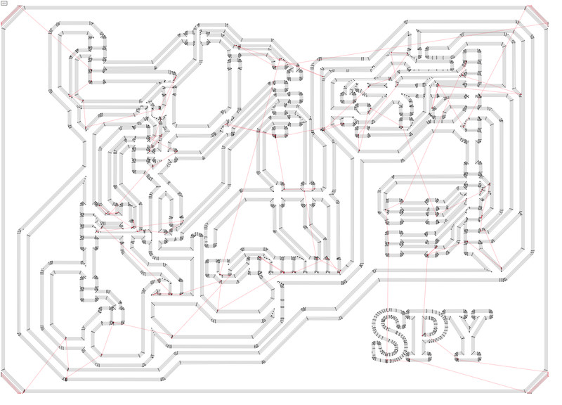
I still had to connect some ratsnest lines. 🙂
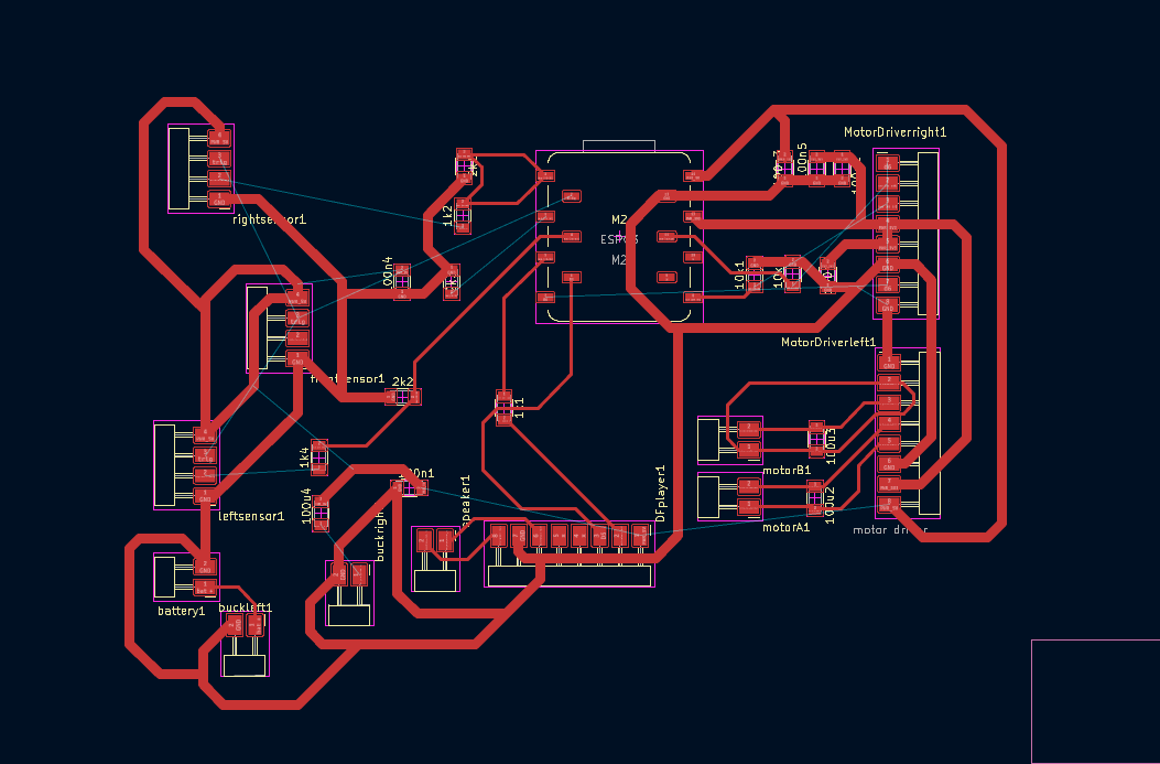
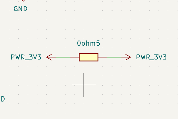
I did not know how to resolve this connection because placing a 0Ω resistor in one of the power nets created additional connections. Sonam Tshering helped me and suggested adding a 0Ω resistor with both ends connected to the 3.3V rail, which solved the issue. Thank you, Sonam Tshering!
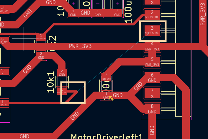
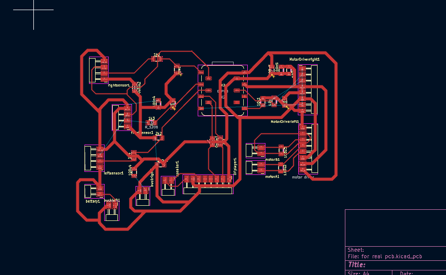
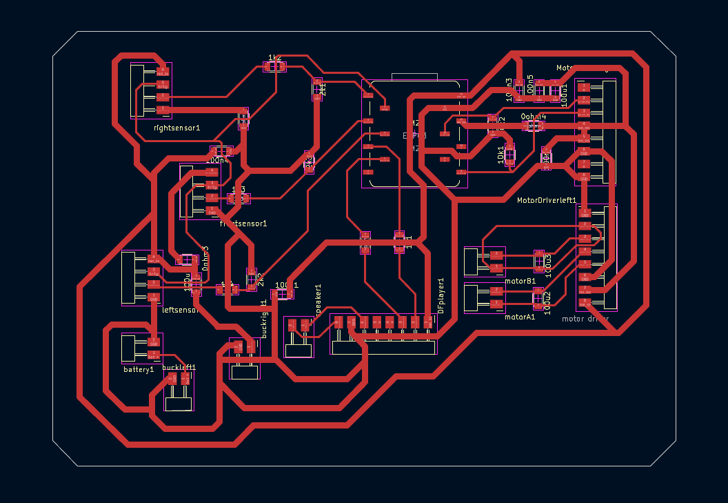
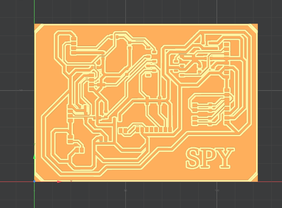
Here is the final PCB layout! 😁
Generating toolpath in MODS CE
After designing the PCB from the schematic, I used Mods CE to generate the toolpath. Detailed steps can be found in my Week 6 documentation. Even though generating the toolpath was not required for Week 6, I had already completed this step earlier, which made this week’s process much easier.
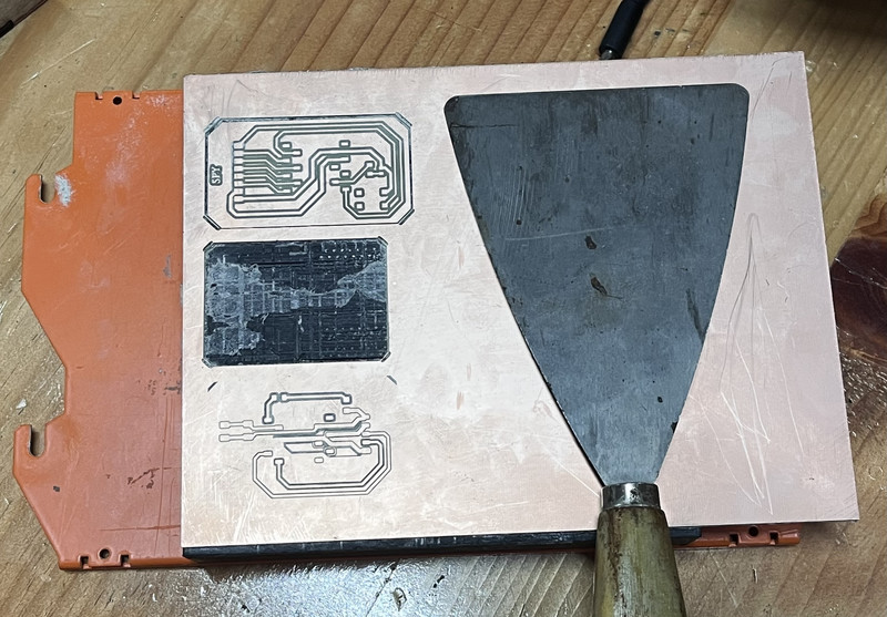
After coming this far, I found out that my PCB had a LOT of short circuits (Thank you Sir Anith for helping me identify them). I also realized that I need to reduce the thickness of my power traces from 1.2 mm to 0.8 mm. Because of these issues, I might just have to re-route the whole thing again 😮💨🤗😫.
This process took up most of my week, so I do not have enough time to redo everything for my final project right now. Therefore, for this week’s assignment, I will focus on designing and fabricating a XIAO ESP32-C3 “hello button blink” board with additional pin headers. I am really sad about not being able to mill out my final project pcb, but I HAVE TO finish the assignment first. 😉
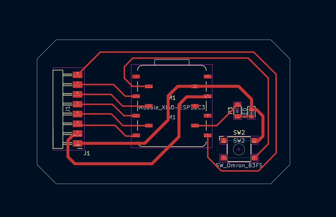
Hello Button Blink Board
I checked out the Fab Academy site and found this reference image on their embedded programming page:
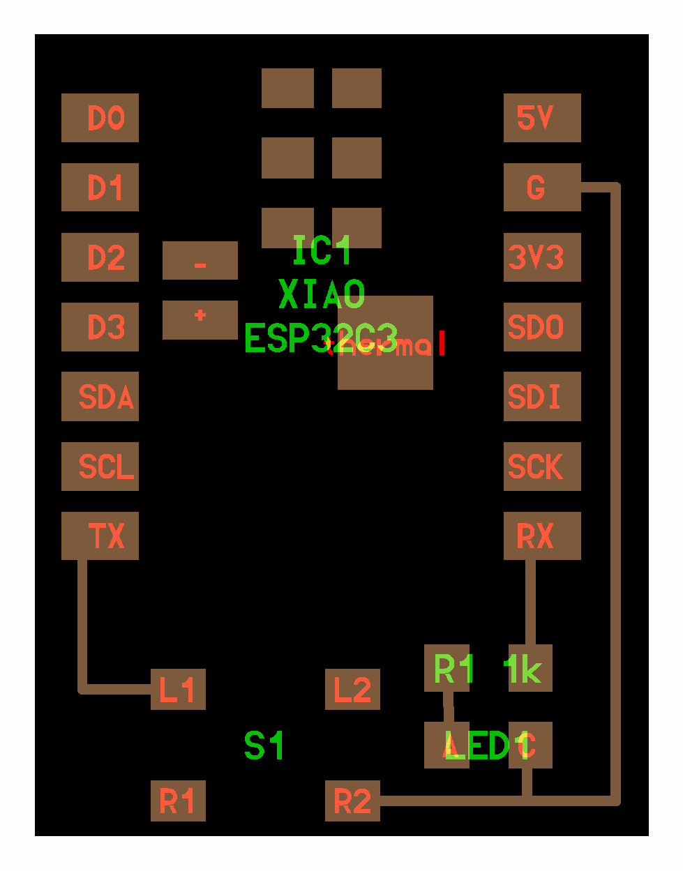
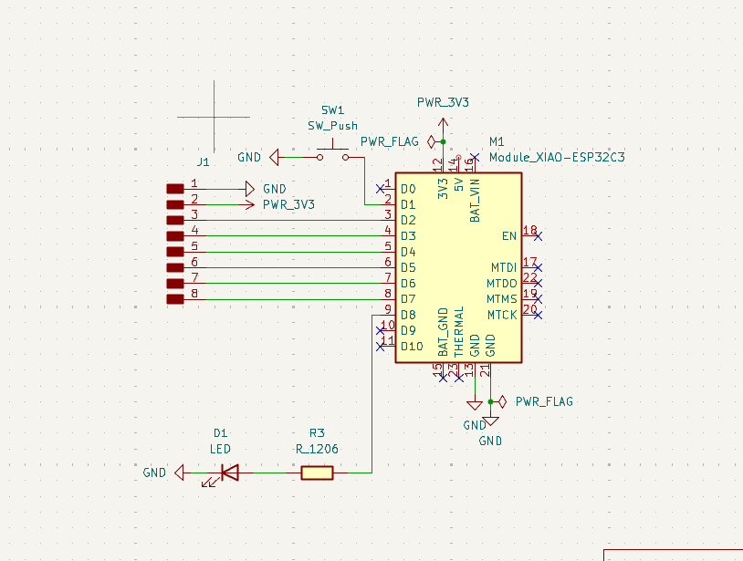
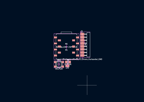
I first started with the schematic design and here is the final layout:
I had less components to route this time so it didn't take a long time 😄 (Thank god)
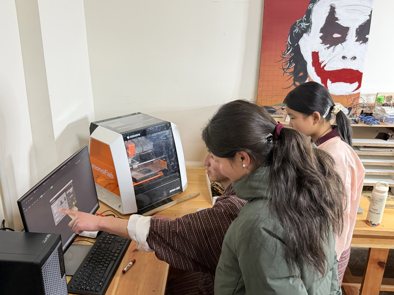
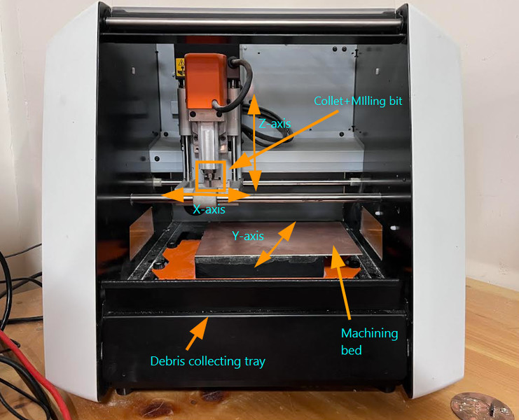
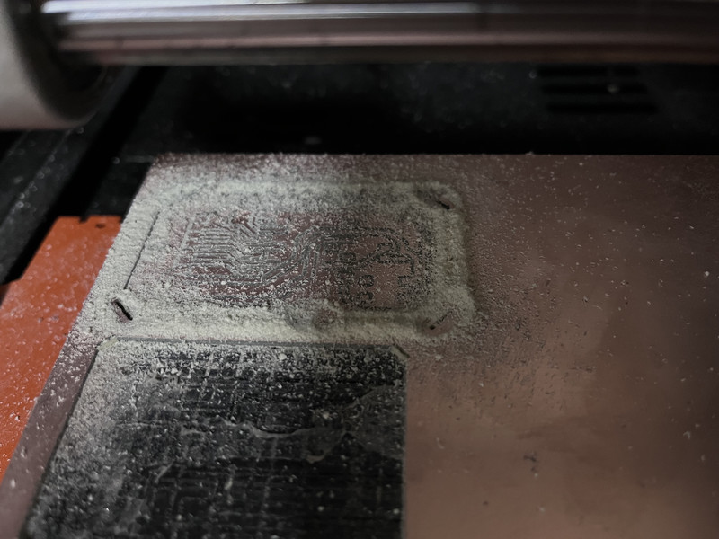
Milling
After I was done creating my rml file using MODS CE, I started with the milling process. The milling machine that we have in our Lab is the monoFab SRM-20. For a more detailed understanding, you can refer to the SRM-20 User Manual .
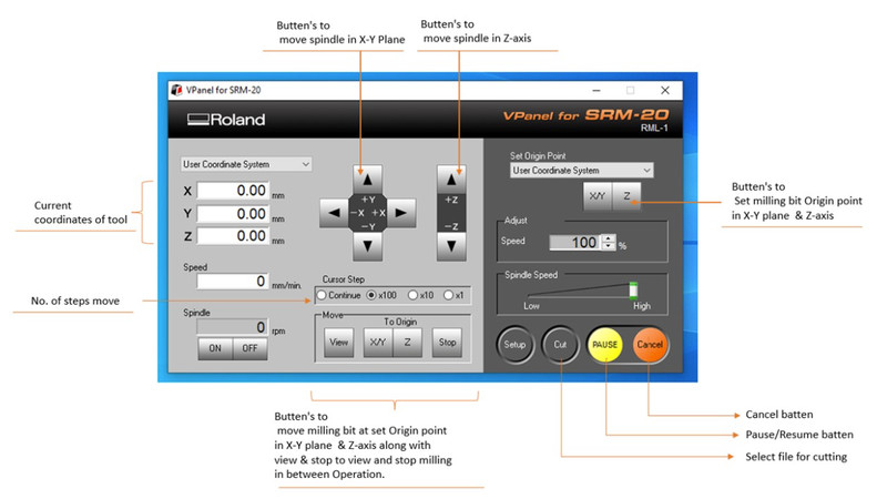
The software used for operating the machine is VPanel for SRM-20
For the PCB, I used FR-1 material. To hold the board in place on the Roland SRM-20, I attached double-sided tape to the back of the PCB and pressed it firmly onto the machine bed so that it does not shift during the milling process.
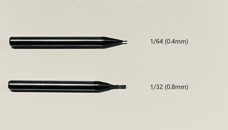
1. Selecting the endmill
First, the circuit traces have to be milled using a 1/64 (0.4 mm) end mill. After that, the tool was replaced with a 1/32 (0.8 mm) end mill to cut the edge cut outline. To change the tool, I loosened the collet, removed the smaller endmill, and then replaced it with the larger one (I made sure that it was screwed properly). The X and Y positions remained unchanged, while only the Z axis is adjusted to match the new tool height.
Since we're doing traces first, I used the 1/64 (0.4 mm) end mill.
2. Setting the X and Y origin
I started by opening the software and ensuring the machine is powered on and connected. I used the control arrows to move the tool head to the position where I wanted the milling to begin. Once it was in the correct spot, I set that location as the X and Y origin using the Set Origin Point ([X/Y]) option.
3. Setting the Z origin
I slowly lowered the tool using the controls until it was just above the surface of the board. Then, I carefully adjusted it by hand using an Allen key until the tool lightly touched the surface. After setting the correct height, I saved this position as the Z origin by clicking on [Z] .
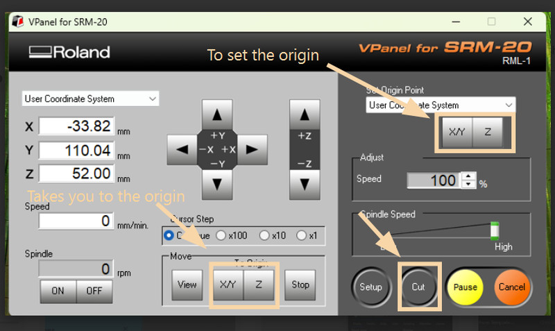
4. Start cutting
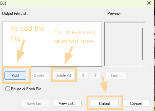
I clicked on Cut and selected my rml file. Don't forget to delete any previously selected files before opening the actual one. You can then click on output and the spindle will start spinning. 🤓
It was so fascinating to watch the spindle move 😄.
Soldering
Soldering is the process of joining 🙏 electronic parts together using melted metal.
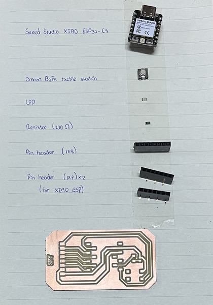
These are the components that I'll be working with 🧑🏭
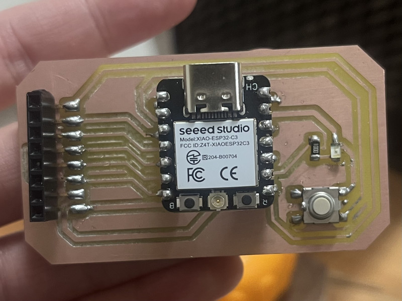
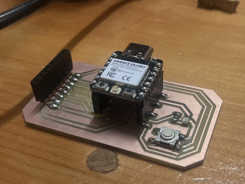
Here is how it looks now! 😄
Soldering Tips & Precautions
- Heat both the PCB pad and the component leg before adding solder
- Apply solder to the joint, not directly to the iron
- Use a small amount of solder (avoid big blobs)
- Keep the soldering iron tip clean
- Don’t overheat components (2–3 seconds is enough)
- Keep the component still while the solder cools
- Check for solder bridges between nearby pins
- Reheat (reflow) joints if something is loose
- Use flux for cleaner and smoother joints
- Make sure connections look shiny and smooth
Programming
I will be using Arduino Ide to program my PCB. I also used it during week4 (Embedded programming week) 🤠
I asked ChatGPT to generate a code for my board. This was the prompt I used: Can you write a basic program where an LED blinks whenever a button is pressed?
const int buttonPin = D1;
const int ledPin = D8;

void setup() {
  pinMode(buttonPin, INPUT_PULLUP);
  pinMode(ledPin, OUTPUT);
}

void loop() {
  if (digitalRead(buttonPin) == LOW) {  // button pressed
    digitalWrite(ledPin, HIGH);
    delay(200);
    digitalWrite(ledPin, LOW);
    delay(200);
  } else {
    digitalWrite(ledPin, LOW);  // off when not pressed
  }
}
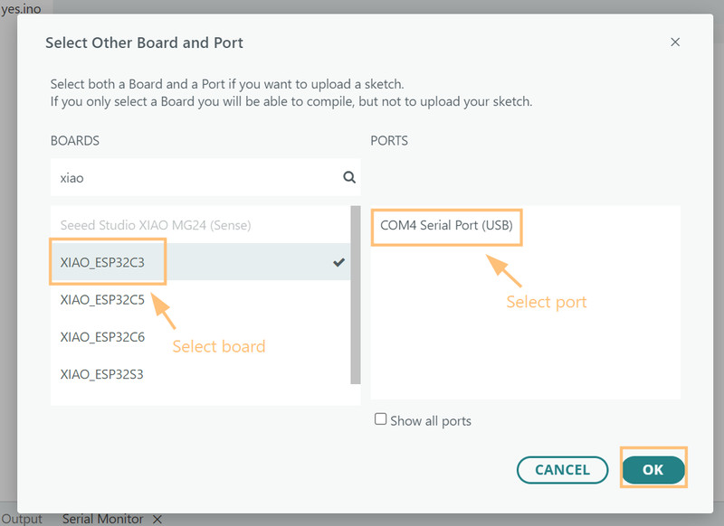
I pasted the code and selected my board, then selected the port.
After that, all I had to do was upload the code 😃
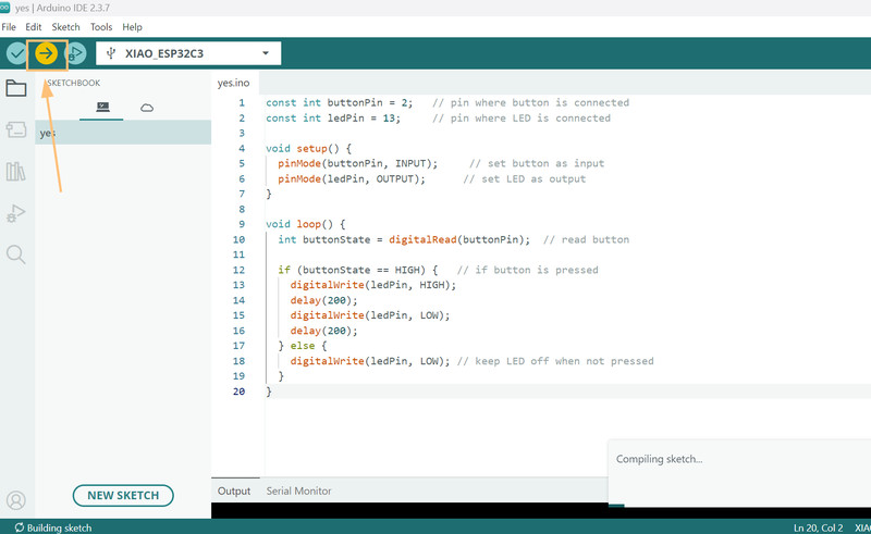
IT WORKED!!! 🥳🥳🥳
Original Design File: Download Week 8 PCB
This week, I felt real panic and and genuinely though that I wasn't going to finish my assignment on time 😅. Even with everything feeling rushed, I still managed to learn a lot. I’m now much more comfortable using the milling machine, which makes me really happy. However, I still need to make some changes to my Final Project PCB. 🫠