
Week 06: Electronics Design
Assignments:
Group Assignment
- Use the test equipment in your lab to observe the operation of an embedded microcontroller (as a minimum requirement, you should demonstrate the use of a multimeter and oscilloscope)
- Document your work to the group work page and reflect on your individual page what you learned.
Individual Assignment
- Use an EDA tool to design a development board that uses parts from the inventory to interact and communicate with an embedded microcontroller
- 3D scan an object (and optionally print it)
Things to Complete This Week
- Document group assignment
- Choose a board to design
- Designing schematic, creating PCB layout, soldering components, and testing the circuit
- Include design files!
Here is my schedule for this week.
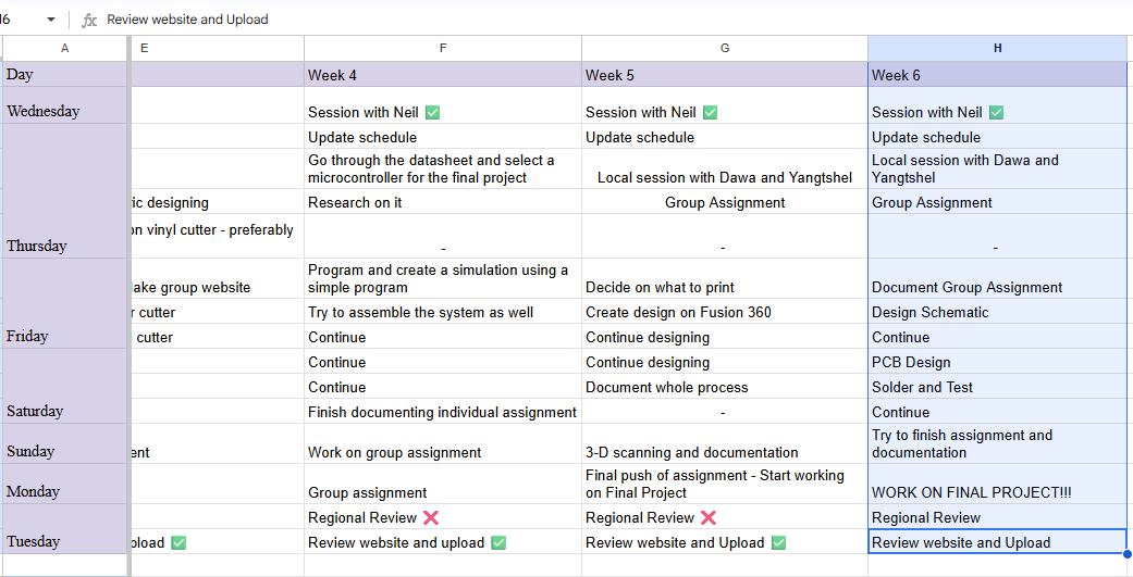
Here is the link to my schedule
Group Assignment
You can access our group assignment here.
This week, we explored the various features and capabilities of the oscilloscope and the multimeter. With the help of our local instructors (Yangtshel and Dawa), not only did we learn a lot, but we also had a lot of fun throughout the whole process 😄.


Individual Assignment
Using Kicad
I have some experience with Kicad (Due to Pre-Fab), so I will be using this software for my assignment this week. Kicad is a free and open-source software tool that is used to design electronic circuits and printed circuit boards (PCBs).

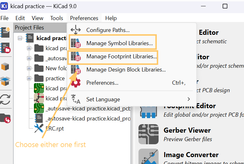
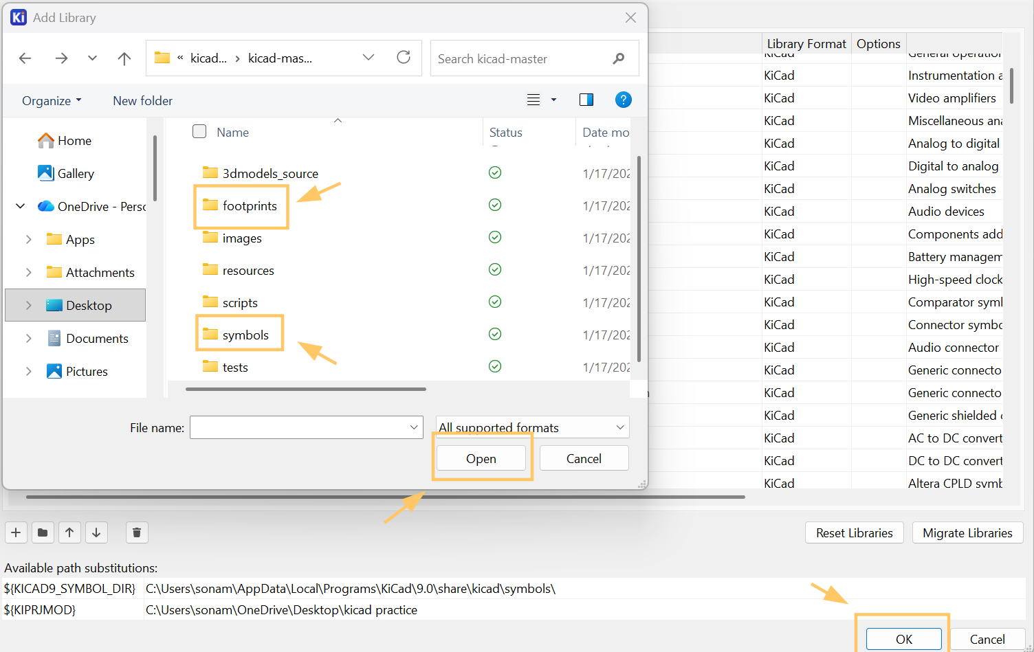
1. Adding libraries in Kicad
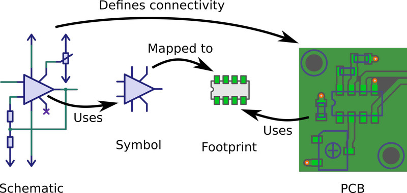
Note: In electronic designing, a symbol is a graphical representation of a component used in a schematic. A footprint, on the other hand, is the physical representation of the same component that is used in the PCB layout.
2. Schematic Designing
This week, I began designing the PCB for my final project 🙂. The ESP32-WROOM-32 will be the main microcontroller of my project.
My goal during this stage was to start developing a reliable and well-organized board that can support all the necessary components for my project.
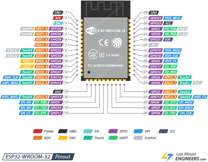
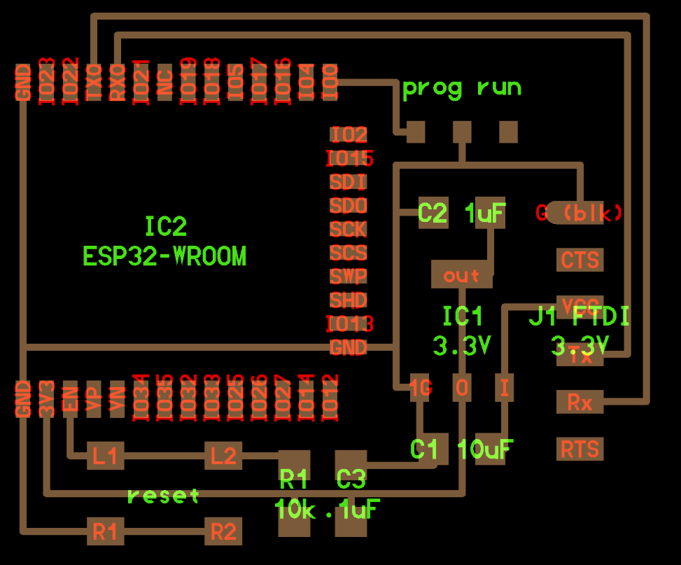
I checked out the Fab Academy site and found the ESP32-WROOM-32's board connection (on their embedded programming page).
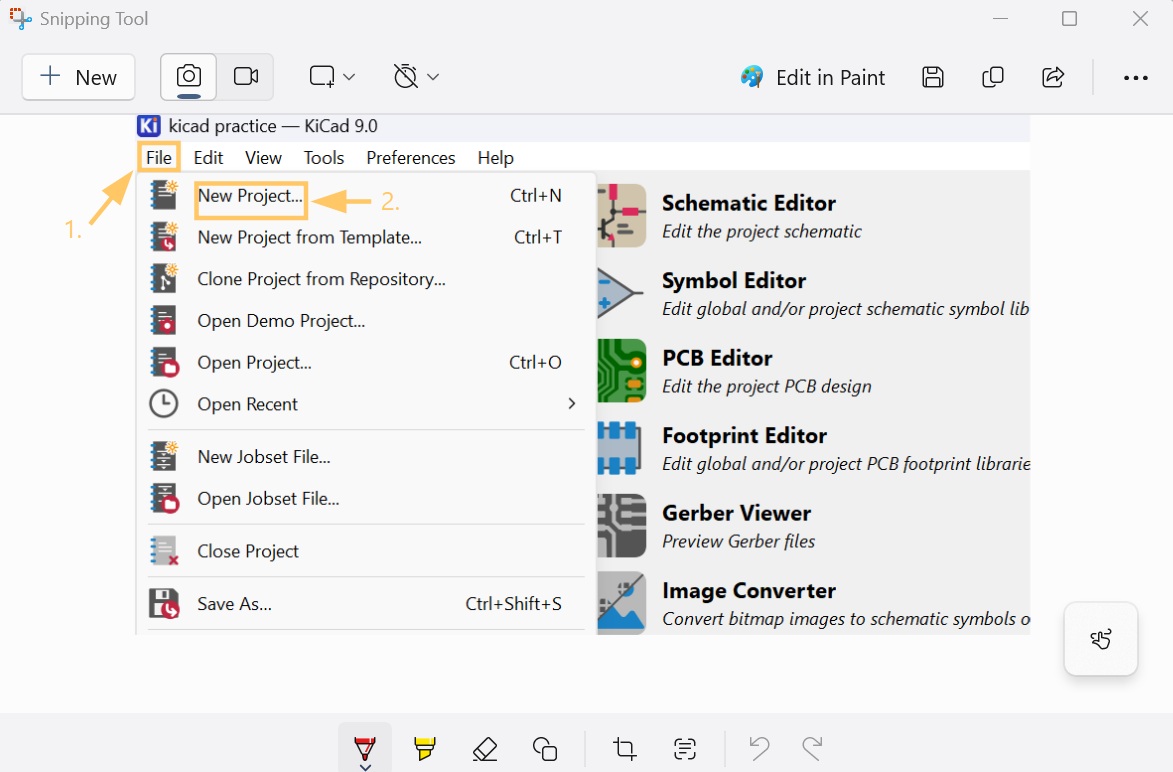
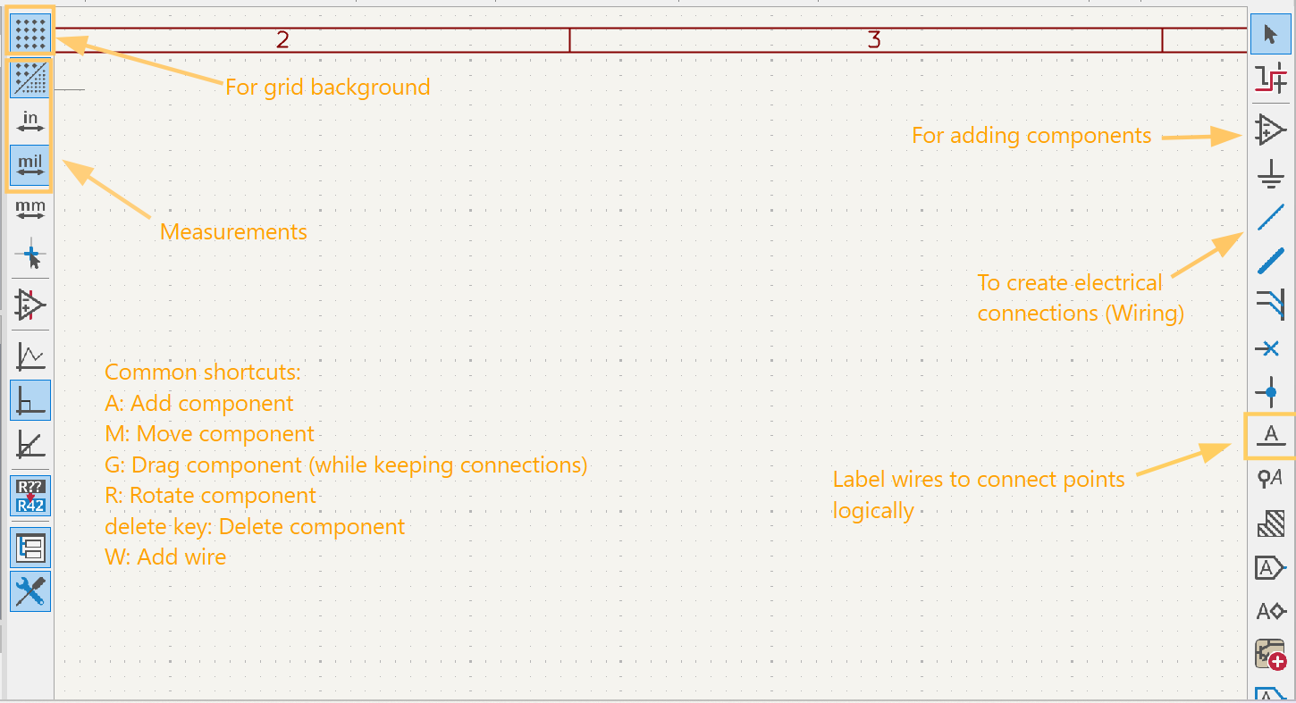
I created a new project and opened the schematic editor. Here are some basic tools and shortcut keys that you can use in Kicad.
I started by designing the circuit connections for the board. Each component in the reference image above is of great importance because the ESP32-WROOM-32 can't operate properly wihtout them. 🤗
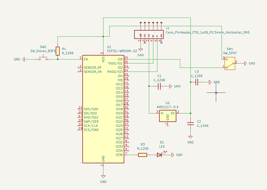
These are the components that I used for the board connections:
| No. | Component Name | Package/Footprint | Quantity |
|---|---|---|---|
| 1 | ESP32-WROOM-32D | Module SMD | 1 |
| 2 | AMS1117-3.3V-1A | SOT-223-3_TabPin2 | 1 |
| 3 | FTDI Header | 1x06 P2.54mm Horizontal SMD | 1 |
| 4 | Push Button | Omron B3SN 6x6mm | 1 |
| 5 | Standard LED | 1206 SMD | 1 |
| 6 | Resistor (100 Ω) | 1206 SMD | 1 |
| 7 | Resistor (10k Ω) | 1206 SMD | 1 |
| 8 | Capacitor (1uF) | 1206 SMD | 2 |
| 9 | Capacitor (10uF) | 1206 SMD | 1 |
I then added the components that I'll be using for my final project. Here is the final schematic look!

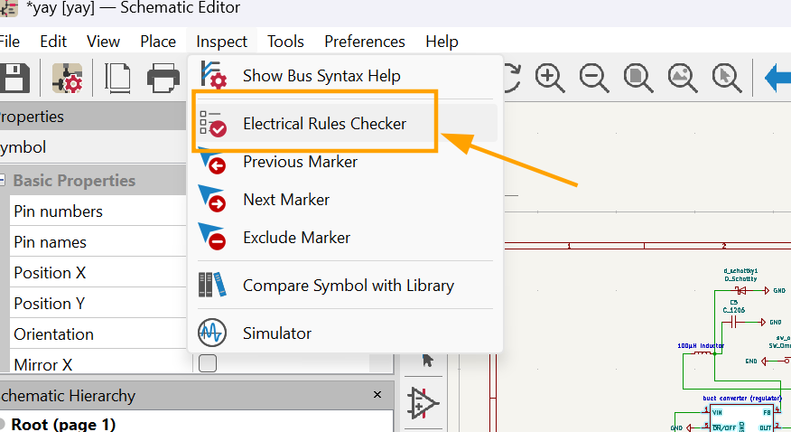
After finishing my schematic design, I ran the Electrical Rule Checker (ERC). The ERC is a tool in Kicad that checks the schematic for electrical mistakes, like unconnected pins or conflicting nets, to ensure the circuit is correctly designed before making the PCB.
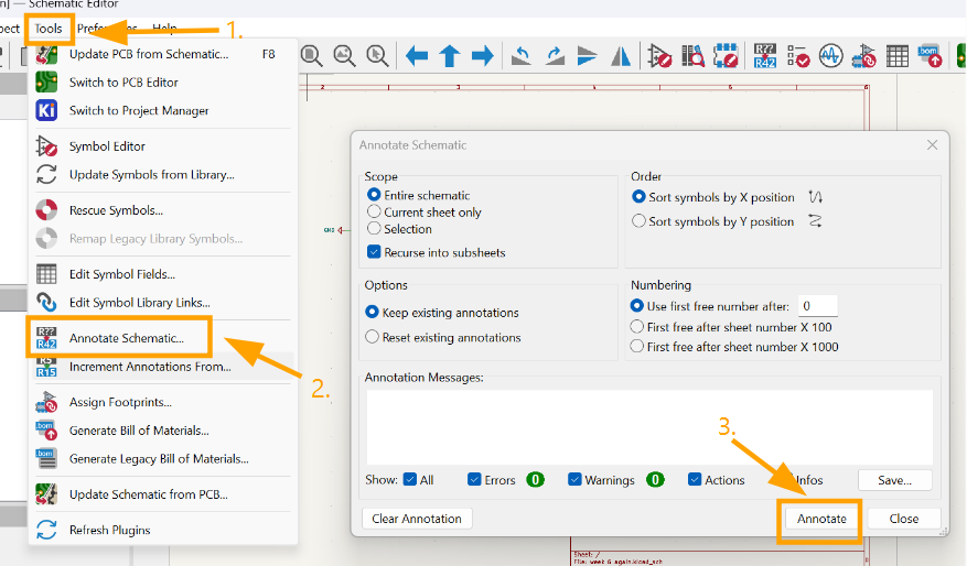
Since I didn't come across any errors, I went ahead and annotated my schematic. Annotation in schematic means assigning unique names to each component so that identifying and organizing them becomes easier 😉.
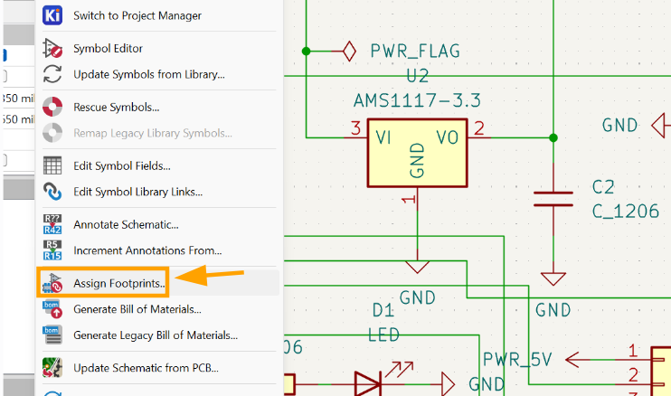
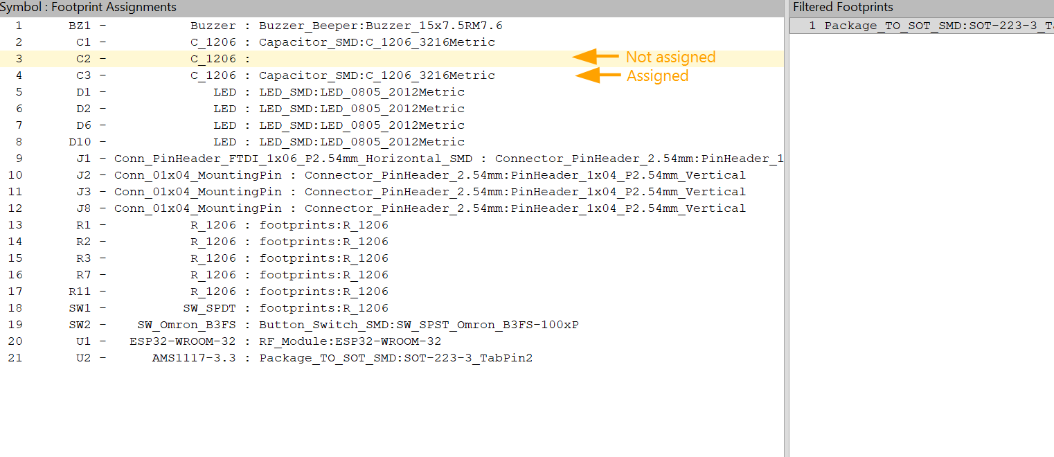
Next I clicked on "Tools" > "Assign footprints" and assigned the respective footprints of each component.
2. PCB Designing
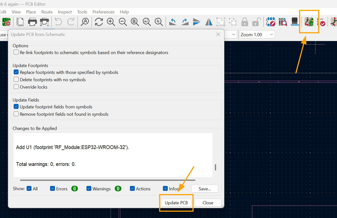
I switched to the PCB editor and updated my pcb.
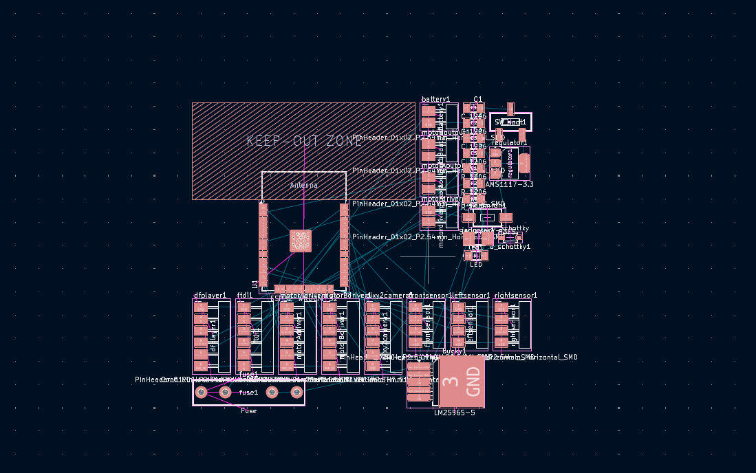
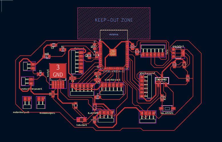
Here is how the PCB layout looks in the editor before the wires are connected. So many components to route!!😱
Routing the board was not at all like what I had anticipated. I thought that as long as I had my schematic design ready, working on the pcb would be a breeze, but it ended up being the hardest part (I underestimated this big time 😭). I also had to use a ton of 0ohm resistors. 😮🙃
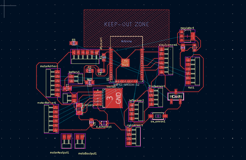
My first try was an absolute disaster. 🙃
My second try turned out to be better than the first, but I still had to work on the placement of some components for better connections.
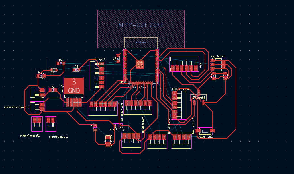
I think the third try came out pretty okay so here is the final look! I had to make use of 10 0ohm resistors 😅, so I'll definitely have to work on modifying this during the weeks that follow.
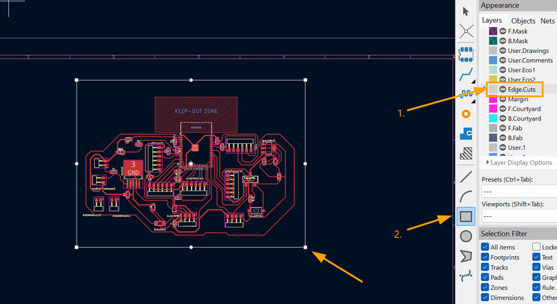
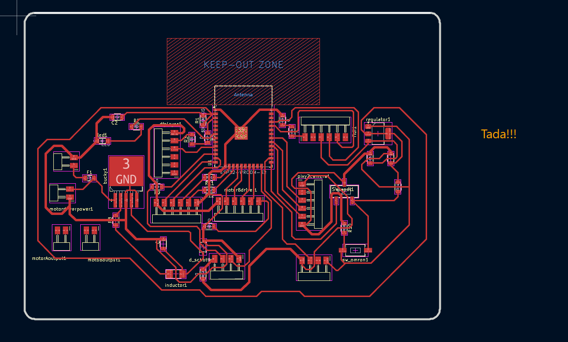
I then edge cut my design.
What is an edge cut?
In PCB designing, an edge cut is the outline that tells the machine where to cut your PCB. It is what defines the final shape of the board.
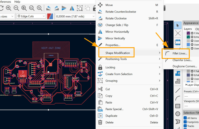
For the edge cut, it is recommended to use rounded corners because they make the board stronger, safer and easier to manufacture. Sharp 90° corners can cause the board to crack easily 🤕. Therefore adding curves allows the board to be cut more smoothly and accurately. To do that, I selected the rectangular outline and right-clicked. Then I clicked on "Shape Modification" and added a fillet of 3mm.
3. MODS CE
Once the schematic and PCB design are complete, the design needs to be converted into RML files. This is done because the Roland SRM-20 milling machine can only read the Roland Milling Language (RML) format. PCB design software like KiCad creates files in the Gerber format (Contains design information about the circuit board), which describes the layout of the circuit board. These files must be converted into RML so that the milling machine can understand the instructions and manufacture the PCB.
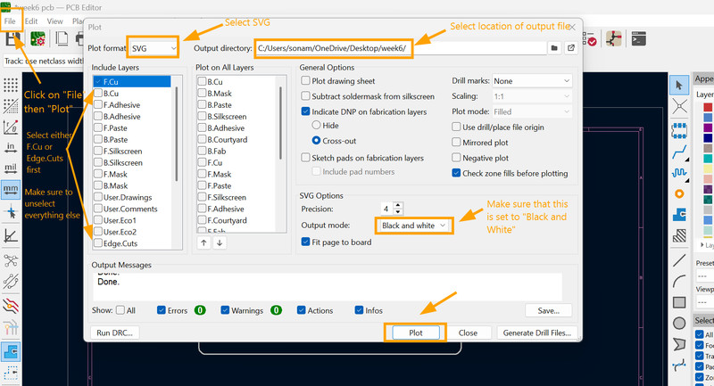
1. I first started by clicking on File > Plot and then used these settings to export my board as an svg file.
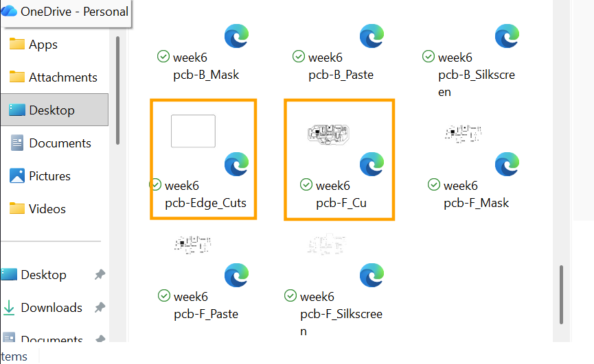
2. Instead of one SVG file, the output is split into multiple different files like this. Only two of the files will be used though.
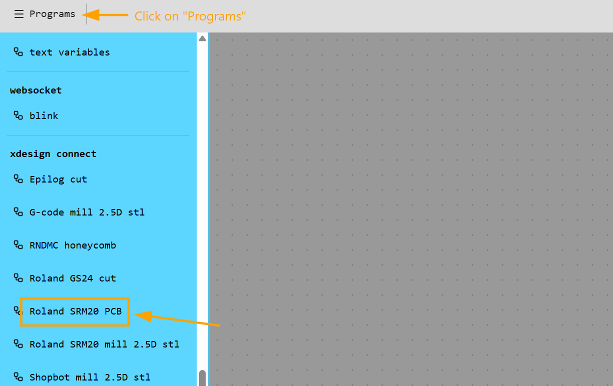
3. I then went onto MODS CE, which is a simple software tool that is used to prepare designs for machines like PCB milling machines. You can use it by clicking on this link. I clicked on Programs and selected Roland SRM20 PCB
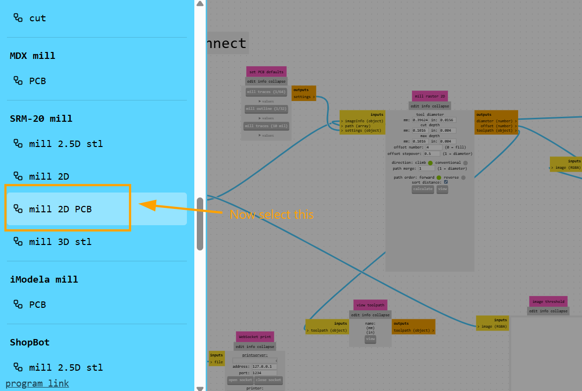
4. After that I clicked on Programs again and clicked on mill 2D PCB
5. I used these settings:
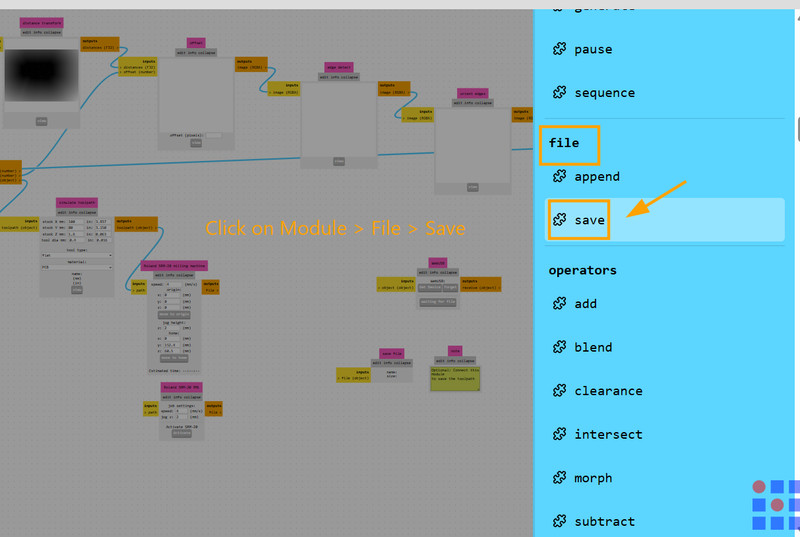
6. Next I clicked on Module and under File, I clicked on Save
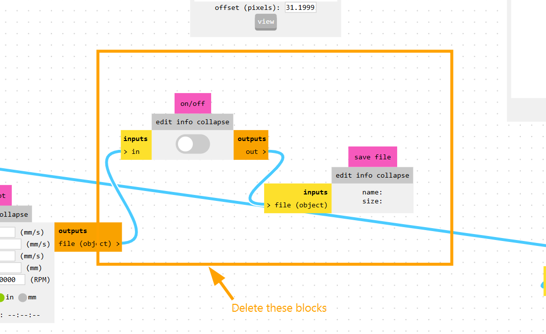
7. I then deleted some unnecessary blocks.
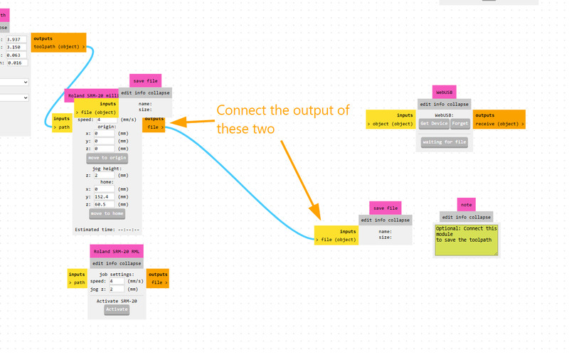
8. After the deletion, I connected the output file to the input file.
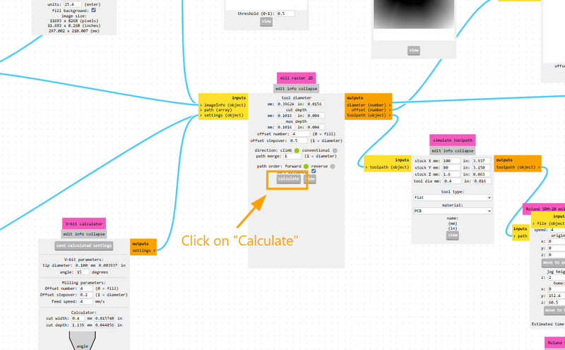
9. Once the settings were adjusted, I clicked on Calculate.
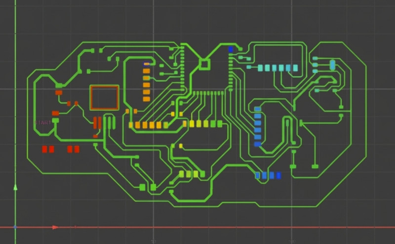
10. Here is how my board looks!!! 😄
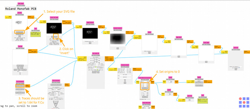
Here are the same steps in order:
1. Insert the SVG or PNG file (I used anSVG file).
2. Invert the image. Inverting means switching the black and white areas of the image.
- This is important because the software treats black areas as parts to keep and white areas as parts to remove during milling.
- By inverting the image, the PCB traces stay protected, while the extra copper around them is milled away.
3. Select “Mill traces by 1/64 inch” since I will be using a 1/64-inch endmill to cut the copper traces.
4. The same process is used for edge cuts, but in Step 3 select “Mill with 1/32 endmill”, since that tool is used to cut the board outline.
5. Set the X, Y, and Z axes to 0.
6. Delete the two unnecessary on/off elements (you can remove them by clicking Edit > Delete). Then right-click and select Add Module.
7. Go to Files, click Save, and connect it to the Outputs file.
8. Finally, press Calculate, and the RML file will be ready for milling.
The board is now ready to be milled!!! 🥳
Note: My initial plan was to mill out the PCB and test it out, but I didn't have enough time 🥲. For this reason, I'll have to do it during WEEK 8 (Electronics Production) or even next week if I can.I feel like this week was the most challenging so far. I definitely underestimated PCB designing 😭 but I have to say that these challenges were exactly what helped me to learn and understand the process so much better. So even though I came to a point where I felt like I would rather program 20 microcontrollers than make one PCB, I am still happy with what I was able to achieve this week.