Electronics Production
Group Assignment
1. Characterize the design rules for your in-house PCB production process
Individual Assignment
1: Make an in-circuit programmer that includes a microcontroller
2: Mill and stuff the PCB
3: Test it to verify that it works
Group Assignment
1. Characterize the design rules for your in-house PCB production process
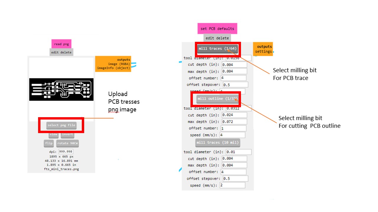
This week we started with group assignment. Our instructor instructed us about PCB milling machine, its setup and modprojects.Details of group assignment are available here.
In our Fab lab, we have Roland Make SRM 20 milling machine. We are using this machine for PCB milling. Fabacademy has given the sketches - Line test and Interior for the precision testing of the PCB milling machine. Using modsproject, we have generated the toolpath. The tool path is uploaded in VPanel. Vpanel is the dedicated software for controlling Roland SRM 20.
We have cut the PCB copper sheet into a size of 150mmx120mm. Double-sided Adhesive tape sticks to the backside of the copper sheet and is placed on the Bed of the milling machine. Leveling of the Bed is ensured with the iPhone level feature. Then we have set up a 1/64" end mill flat tool in the collet to trace the path in the PCB. Using gravity technique, we have ensured that the tool's tip is touched to the top of the copper plate. And we set the tool position [X,Y,Z]=[0,0,0] local coordinate system.
After finishing tracing operation, 1/32" tool is employed in the collet and again using gravity test procedure, we set coincident tooltip position with the copper plate as the origin for this tool path. After finishing the operation, the material removed taken out with a vacuum cleaner. And with the help of a scrapper, the final part is removed from the Bed of the milling machine.
.png)
Conclusions of group Assignment
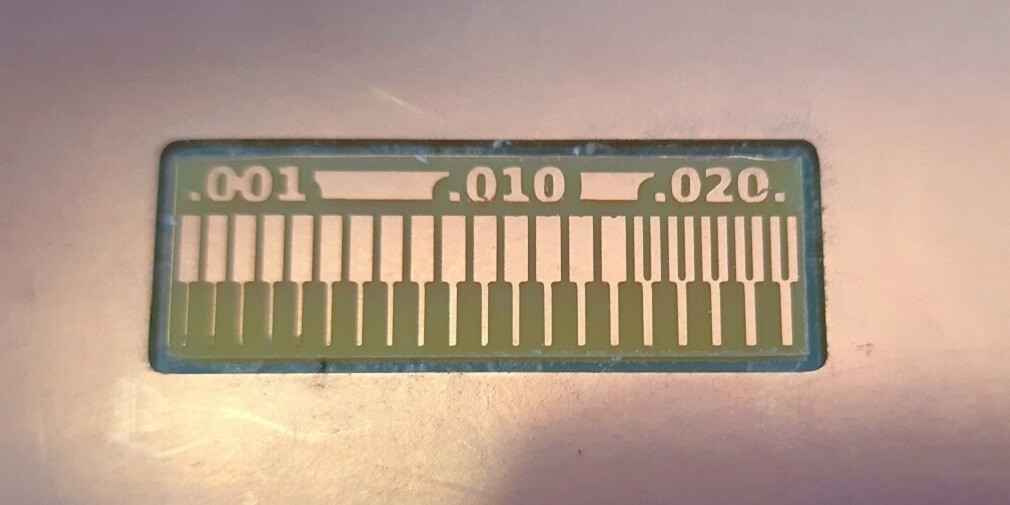
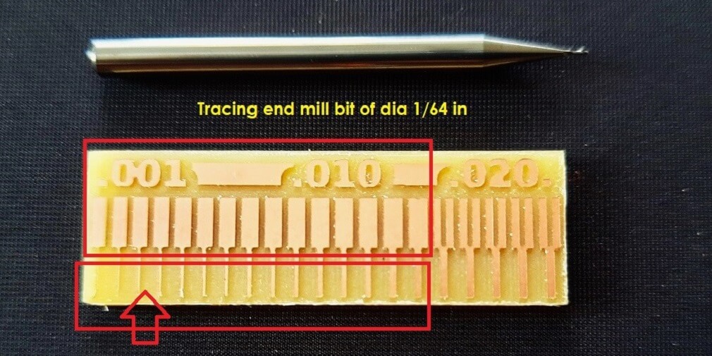
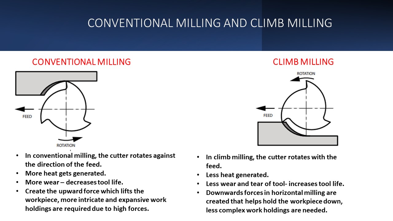
1. The gap between two traces has to be more than the tool diameter. In our case, the tool diameter was 1/64 inch, i.e. 0.0156 inch, the tool did not create traces, where the gap between two traces was less than 0.0156 inch. The CAM software itself does not create the tool path, where the gap between two traces is less than the tool diameter.
2. The minimum width of the trace has to be little more than the tool diameter. In our case, the tool diameter was 1/64 inch, i.e. 0.0156 inch. The traces were not cut properly, where the trace width is less than 0.0156 inch. Towards the left side of the board, where the trace widths are gradually decreasing, the tool could not cut the trace properly. The traces were removed off of the surface, which is not a good practice of machining PCB.
In this week our task is to make fabisp and to program it. As a Mechanical Engineer and because of very little awareness about electronics, I thought this would be challenging. I have not even soldered any component before coming here. But our instructor encouraged and guided all of us to complete this week's assignment.
Some basic concepts
This week, my task was to manufacture the PCB for the in-system programmer consisting of a Microcontroller. All the terms ISP, Microcontroller and PCB are new to me. So I started learning about these terms.
In-system programming (ISP)
In-system programming (ISP) is the ability of some programmable logic devices, microcontrollers, and other embedded devices to be programmed. At the same time, they are installed in a complete system, rather than having to program the chip before it is installed. It also simplifies design work by allowing firmware upgrades to be transmitted to the on-chip memory of microcontrollers and similar processors without the need for specialized programming hardware on the circuit board.
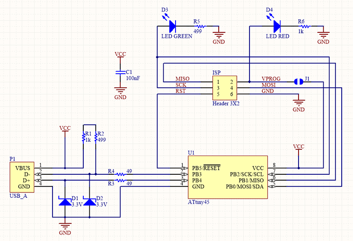
In this week, we have choices to develop any ISP. I have decided to FABISP by Brian. This ISP consists of an ATtiny45 microcontroller.
ATtiny45 Microcontroller
ATtiny (also known as TinyAVR) are a subfamily of the popular 8-bit AVR microcontrollers.AVR is a microcontroller family created by Atmel in 1996. These are 8-bit RISC single-chip microcontrollers with a modified Harvard design. AVR is one of the first microcontroller families to employ on-chip flash memory for program storage.
ATtiny45 Specifications
The high-performance, low-power Microchip 8-bit AVR® RISC-based microcontroller combines 4 KB ISP Flash memory, 256B EEPROM, 256B SRAM, six general purpose I/O lines, 32 general purpose working registers, one 8-bit timer/counter with compare modes, one 8-bit high-speed timer/counter, USI, internal and external Interrupts, 4-channel 10-bit A/D converter, programmable watchdog timer with internal oscillator, three software selectable power saving modes, and debugWIRE for on-chip debugging. The device achieves a throughput of 20 MIPS at 20 MHz and operates between 2.7-5.5 volts.
PCB
A printed circuit board, or PCB, is used to support mechanically and electrically connect electronic components using conductive pathways, tracks, or signal traces etched from copper sheets laminated onto a non-conductive substrate. Components are generally soldered onto the PCB to both electrically connect and mechanically fasten them to it.
PCB Manufacturing Techniques:
Chemical Etching
The chemical PCB etching is a subtractive manufacturing process in which material is removed to generate the requisite electrical separation and ground planes.
With chemical etching, high-quality circuit boards can be created for different applications. In the chemical etch process, the precision and quality of the mask used to shield the copper from the chemicals and the condition of the etching chemicals determine the quality of the circuit board. This process is suitable for Large production.
Milling
Printed circuit board milling is the manufacturing process of removing copper from a sheet of printed circuit board material to reconstruct pads, signal lines, and structures based on patterns from a layout file.
PCB milling, unlike chemical etching, is usually a non-chemical operation that may be conducted in a conventional office or lab setting without exposing workers to dangerous chemicals. The milling accuracy and control of the system and the condition of the milling bits and their corresponding feed/rotational rates affect the quality of a circuit board in PCB milling. PCB milling is suitable for prototype Application
Machining any component on a milling machine can be machined in two ways. 1. Climb Milling 2. Conventional Milling.
CONVENTIONAL MILLING AND CLIMB MILLING
PCB Milling Machine
Vigyan Ashram is having Rolland make SRM 20 CNC milling Machine.
An SRM-20 milling machine is a compact machine with excellent capability at an economical price. Creating realistic components and prototypes is straightforward and comfortable with a device that fits into any workplace, home, or school environment. The SRM-20 is the most accessible and precise CNC mill in its class for consumers searching for sophisticated milling capabilities without professional operating skills.
Machine Specifications
| SRM 20 CNC milling Machine Specifications. | ||
|---|---|---|
| MODEL | SRM-20 | |
| Cuttable Material | Modeling Wax, Chemical Wood, Foam, Acrylic, Poly acetate, ABS, PC board | |
| X, Y, and Z Operation Strokes | 203.2 (X) x 152.4 (Y) x 60.5 (Z) mm | |
| Workpiece table size | 232.2 (X) x 156.6 (Y) mm | |
| Distance From Collet Tip to Table | (130.75mm) | |
| Loadable Workpiece Weight | 4.4 lbs (2kg) | |
| X-, Y-, and Z-Axis Drive System | Stepping motor | |
| Operating Speed | 6 – 1800mm/min | |
| Software Resolution | 0.01 mm/step (RML-1), 0.001mm/step (NC code) | |
| Mechanical Resolution | 0.000998594 mm/step | |
| Spindle Motor | DC motor Type 380 | |
| Spindle Rotation Speed | Adjustable 3,000 – 7,000 rpm | |
| Cutting Tool Chuck | Collet method | |
| Interface | USB | |
| Control Command Sets | RML-1, NC code | |
| Power Requirements | Machine: DC24V, 2.5A, Dedicated AC adapter: AC 100-240V ±10%, 50/60Hz | |
| Power Consumption | Approx. 50W | |
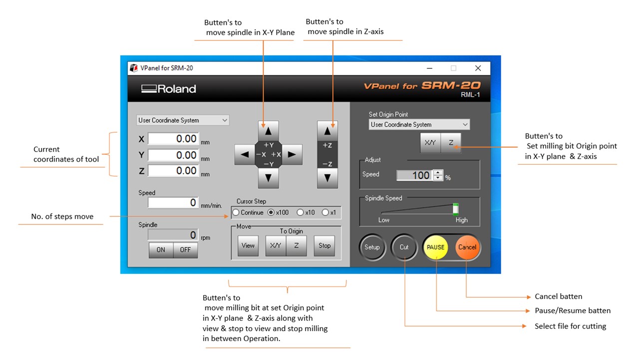
VPanel Dashboard
Vpanel is the dedicated software for controlling Roland SRM 20. The machine is connected to the computer through the USB connection, and the machine is controlled by Vpanel software. With the help of this software, we can come the spindle in X/Y/Z direction, control tool rotation and tool transverse speed, move the spindle along the local co-ordinate system, and program the machine to move the spindle with the specified path.
Source: https://www.rolanddg.co.in/products/3d/srm-20-small-milling-machine/features
Accessories required to set up the machine
Individual Assignment
This week, we have the option of developing any ISP. I've chosen to FABisp Brian's work. All of the information on Brian's FabISP is available here.
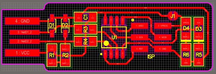
Because this week is all about PCB manufacturing, Fab Academy has already provided the PCB design.
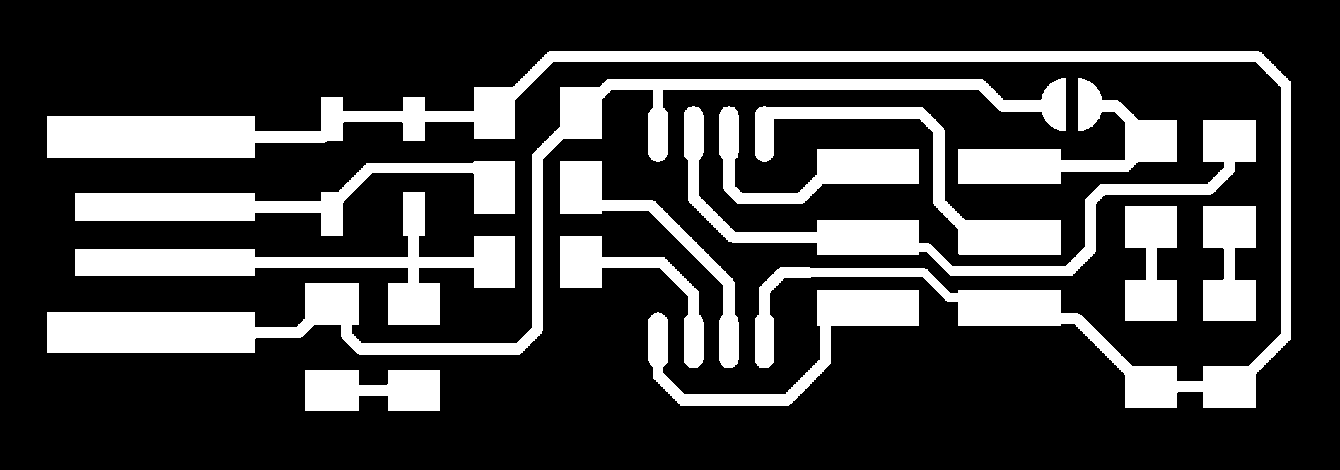
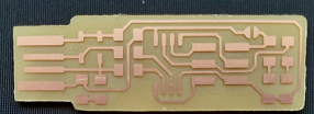
.png)
.png)
Original sketches can be download here.
PCB Traces
PCB Cutout
Tool Path Generation
After having the sketches, the next task is to generate the tool path or NC code. Here we are using a modsprojects web-based application recommended by Fab Academy.
modsprojects have inbuilt libraries for different machines used in Fab Labs, and it interfaces with the machine to perform tasks like Milling, Vinyl cutting etc.
Here I am generating the tool path using modsprojects for Roland SRM 20 Milling machine to trace the path and cut the outline of the PCB.
I have entered the http://modsproject.org/ link in the my Microsoft edge browser. And then, I have selected the SRM 20 machine with the PCB Absolute program.
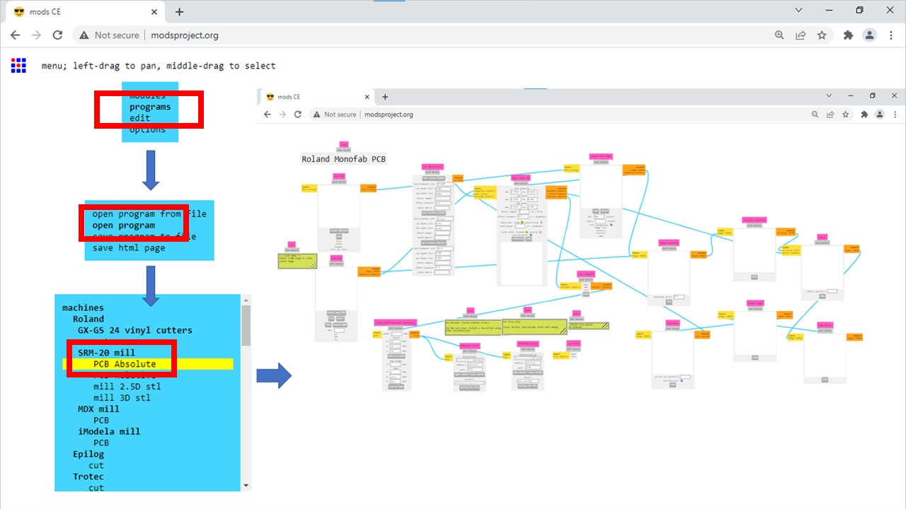
Then I have selected and uploaded the PCB trace file using the select png tab.
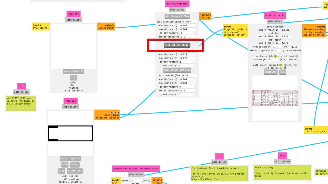
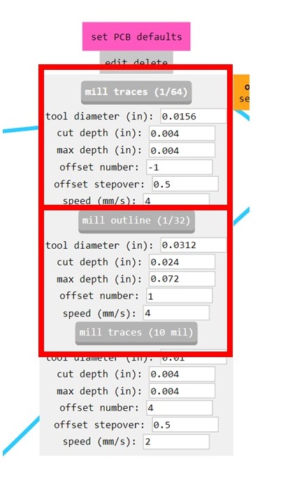
Then I have selected the Mill traces (1/64) option to trace the path in the PCB.
Next, the Save file block was added to save the tool path (NC code).
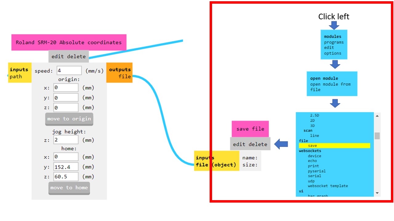
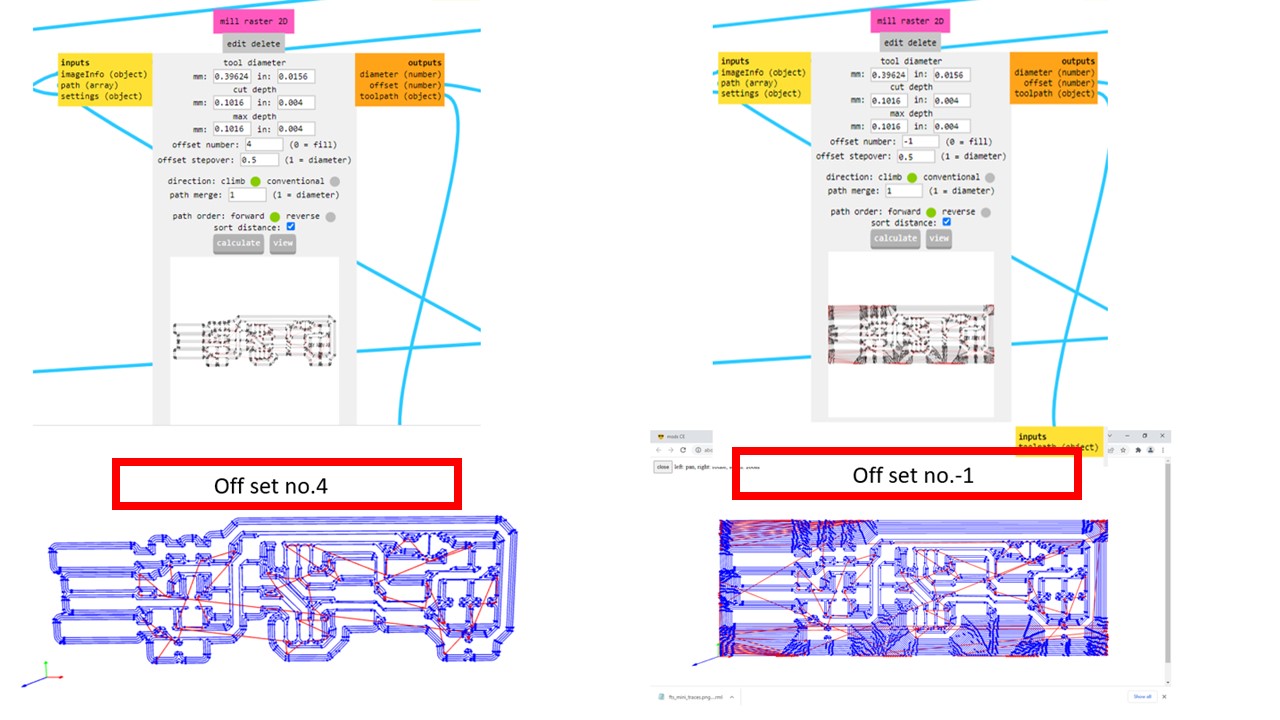
Offset number -1 is selected to get the required trace without any other mark of copper clad on the PCB except traces.
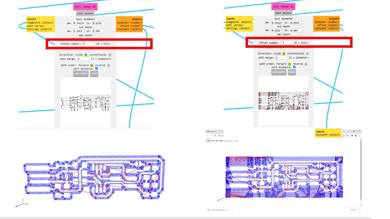
And at last, I clicked on Calculate tab to download the toolpath as a .rml file.
To cut the PCB from Copper FR1 Phenolic plate mounted on PCB milling machine. Now, .png file was elected to cut the outline of the PCB.
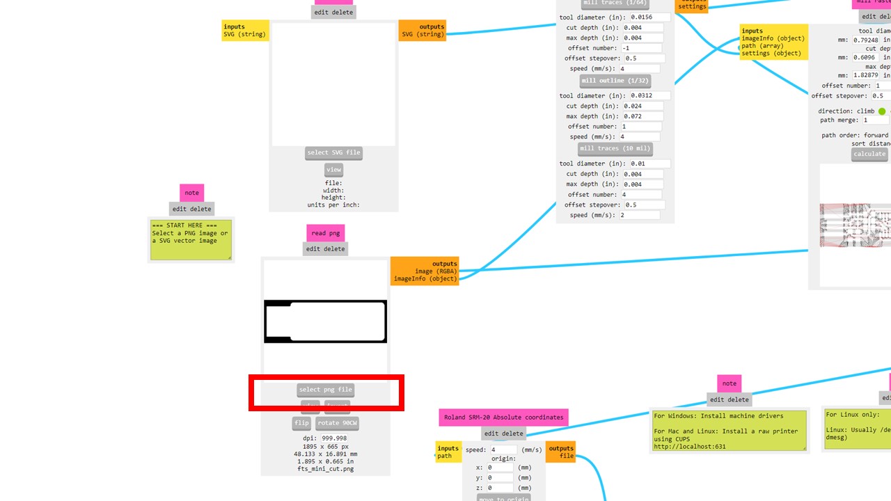
Then the clicked on Mill outline (1/32) tab and selected parameters for the workpiece.
Nect, clicked on the calculated and automatically .rml file is generated and downloaded in computer.
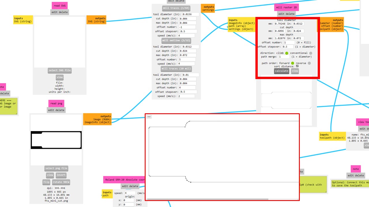
Parameters selected for cutting and tracing are shown here.
Detailed Description of group assignment can be found here
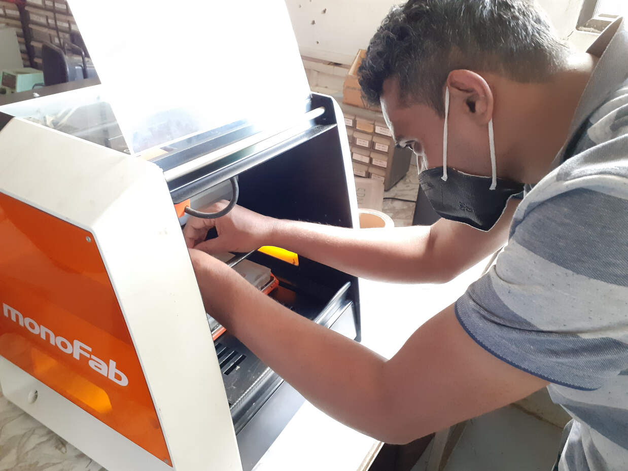
Machine Setup for PCB Milling
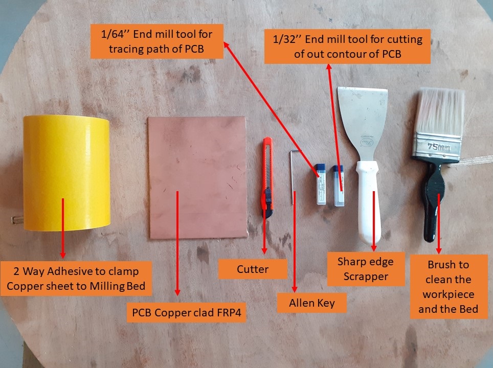
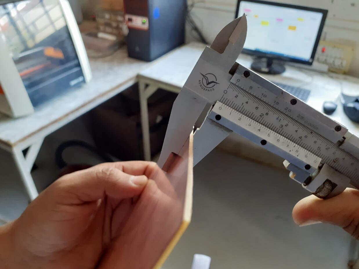
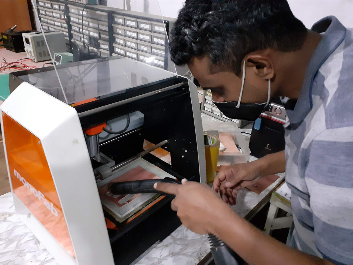
After the generation of the tool path, next, I started to set up PCB MILLING MACHINE. I have cut the FR1 copper clad sheet of 100mmx100mm, which will fit the bed size of the milling machine. I have measured the thickness of the sheet. Because sheet thickness may vary with the manufacturer. Measure sheet thickness was 1.8mm
Next, I have set up the 1/64'' diameter, end mill flat milling tool to mark the traces on the Copper clad plate.
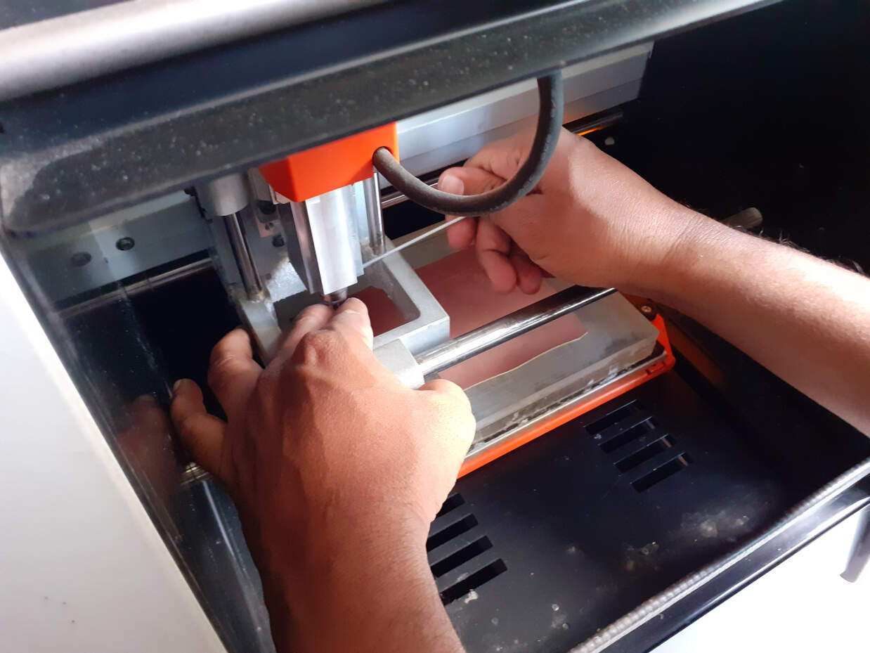
There are two types of the coordinate system used in the Milling machine. Machine Coordinate System (MCS) (Global Co-ordinate system) Local Coordinate system. Machine Coordinate System (MCS) represents an abstract coordinate system. It is not bound to a fixed point of the machine. All other coordinate systems refer to this coordinate system. But when we want to perform any operation on the workpiece at a specific location, we need to move the tooltip to that position set it to all the X/Y/Z coordinates (0,0,0). This point will be the origin of a particular part. We developed the program from the same position with an absolute position system
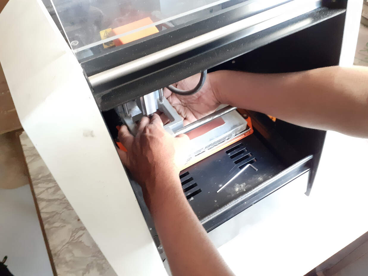
Then with the VPanel, spindle moved to the required position and set (X, Y) origin. This is the point from where the machine will start milling operation. Then Machine Setup Gravity test. We required 3-4 operations that required different tool bits set up to make the PCB. As this is a manual process, we need to make sure that the tip of the tool bit touches the PCB plate to make it local origin from which we wish to start machining, and we have already set up the tool path from the same position. For this purpose, we need to gravity drop procedure: Change the tool bit Move tool X/Y -set X/Y origin position ON VPANEL. Move Z-Axis till the tool bit is just away from the PCB plate. Then release the tool bit from the collet allow the tooltip to touch the top of the plate. Then SET this position is Z- origin position ON VPANEL We need to follow the same procedure whenever we change the tool.
Using the cut feature of the Vpanel, the program file generated from modprojects uploaded in the system And started the operation for PCB tracing shown in the video.
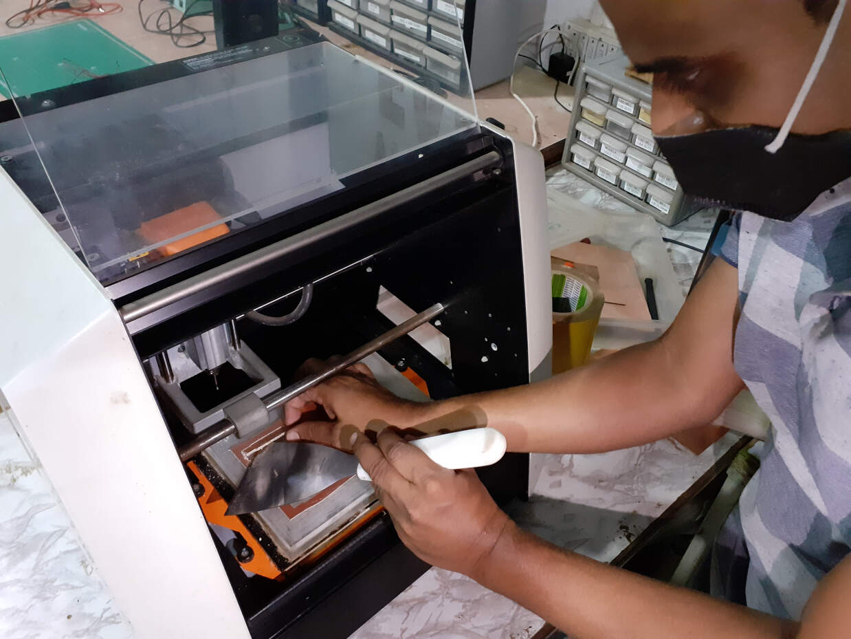
Next to clean the bed and workpiece with vacuum cleaner.
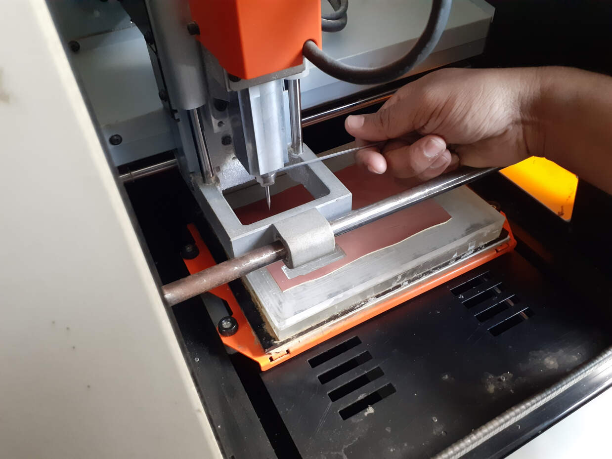
This is the final PCB tracing operation.
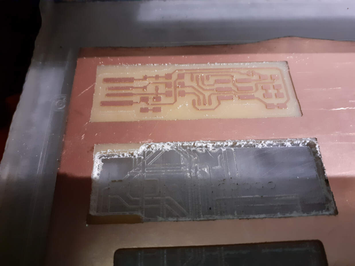
Then new 1/32" tool is set up to remove traced PCB from the workpiece. Again followed the procedure of Gravity test, (X, Y, Z)=(0,0,0) and uploaded cutout program. Start the contouring operation. The following image is the image after performing the cutout operation.
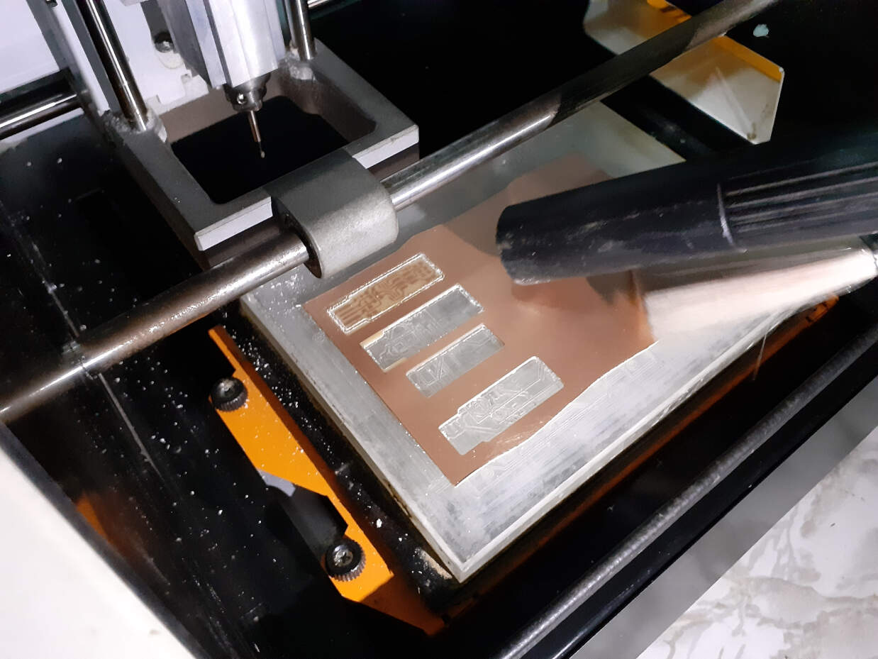
Excessed material removed from the copper-clad cleaned with the Vacuum cleaner and brush. And final traced PCB is removed from the bed with the spatula shown here.
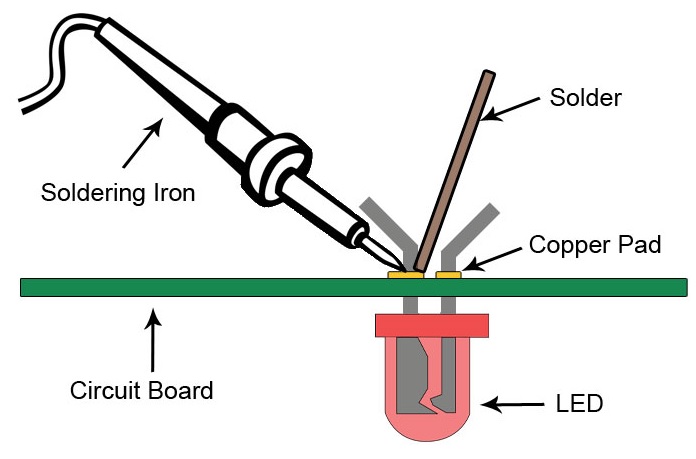
Soldering
Soldering is a metal-to-metal joining procedure in which solder is melted and used to connect different types of metals. Solder is a tin and lead-based metal alloy that is melted with a hot iron. The iron is heated to above 600 degrees Fahrenheit and then cooled to form a strong electrical connection.
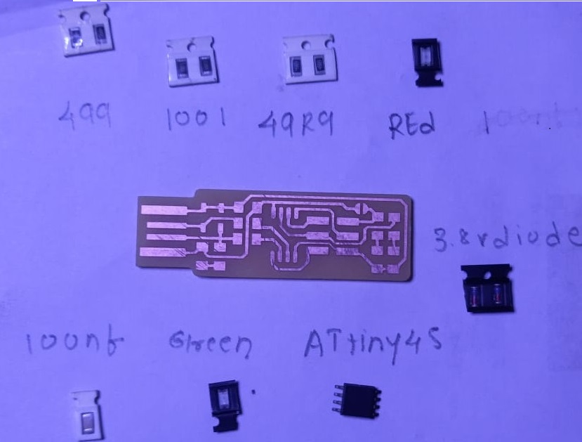
List of components required for FABISP. The list is already given by FAB Academy.
1x ATtiny45
2x 1kΩ resistors
2x 499Ω resistors
2x 49Ω resistors
2x 3.3v zener diodes
1x red LED
1x green LED
1x 100nF capacitor
1x 2x3 pin header
Soldering Operation
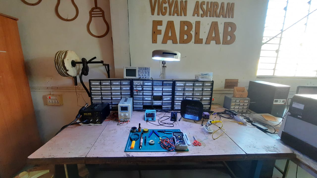
Fab Lab Vigyan Ashram has state of art Soldering Station facility.
Soldering station consist of All the essential equipments required for the soldering.
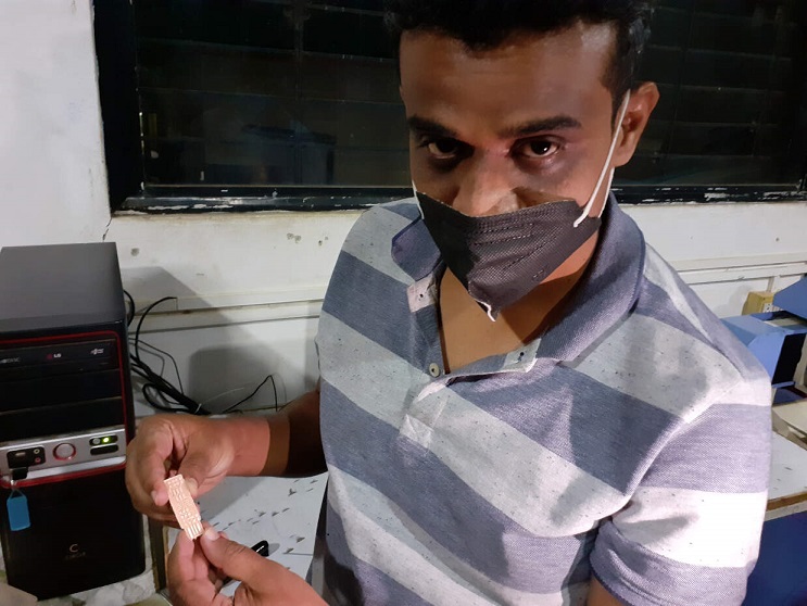
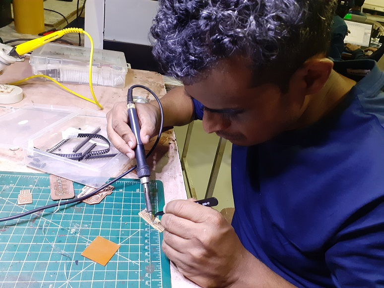
I was handling solder Gun SMD's for the first time, so it was a mixed reaction for me. I want to learn something new and get scared about the failure of soldering. But Instructor has given very nice training in soldering. So we got some confidence in soldering. Initially, we tried to do soldering of SMD's on trial PCB, and After gaining some confidence, I tried on my FABISP PCB.
To mount the component's incorrect orientation, I referred to brian documents where I got the circuits to design both schematic and PCB design. Using this design, I can stuff my components correctly with proper polarity.
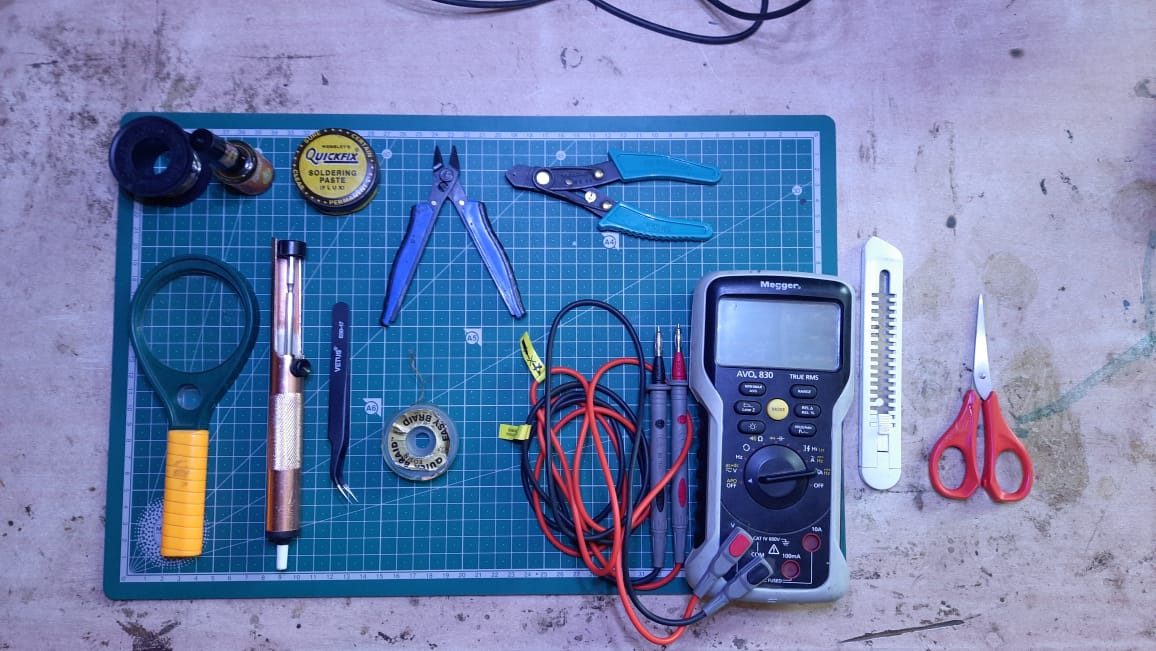
The soldering workstation consists of a Weller make soldering station with a temperature controller, solder wire, flux, Hot gun, Stripper, tweezer, Multimeter, cutter, etc.
It takes some time time to settle with the gun. I tried solder SMDs on trial pieces given by our instructor, which helped build confidence during soldering. During soldering, also I failed to solder a lot of time. By practicing and with patience, I could complete the PCB soldering.
And my final job is ready to test.
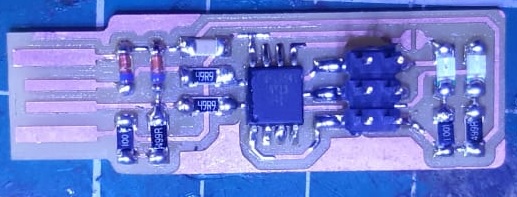
I used the multimeter to check all the connections and verified no dry solder. Luckily everything was working perfectly.
Software Installation
I needed to set up my development environment before compiling and programming the firmware into my board. This is where I'll be doing all of my AVR programmings for the lesson. The setup varies slightly per platform, but it should work similarly on all platforms once the program is installed.
I have used Brians Document Brians Document to install the software in the system.
Install Git- GIT
Install the Atmel GNU Toolchain-Atmel GNU Toolchain
Install GNU Make-GNU Make
Install avrdude -AVRDU
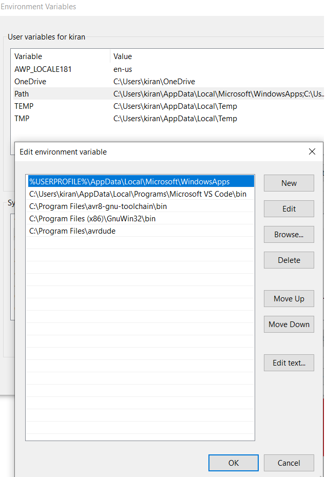
Update your PATH-
The three values to add are:
C:\Program Files\avr8-gnu-toolchain\bin
C:\Program Files (x86)\GnuWin32\bin
C:\Program Files\avrdude
Install Drivers for your Programmer -Zadiag
Sanity Check
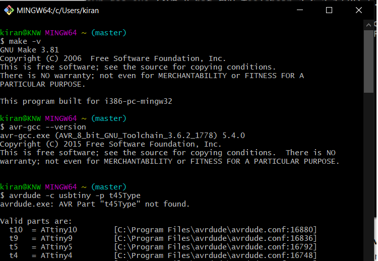
This shows that everything is installed in the system.
Programming the programmer
Week Outcomes:
Get and Build the Firmware: Download the firmware source code, click here and extract the zip file (fts_firmware_bdm_v1.zip). Open your source code directory and open Git bash from this folder.
Run 'make' command in Git bash. This will build the hex file that will get programmed onto the ATtiny45. When the command completes, you should now have a file called fts_firmware.hex.
plug the board into a USB port:
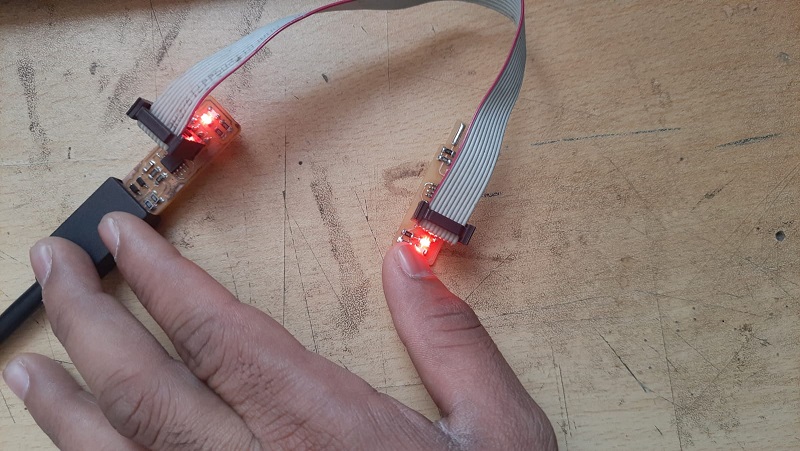
plug the board into a USB port:Red LED lit up means soldering connections are ok.
Run make flash. This will erase the target chip, and program its flash memory with the contents of the .hex file you built before. You should see several progress bars while avrdude erases, programs, and verifies the chip.
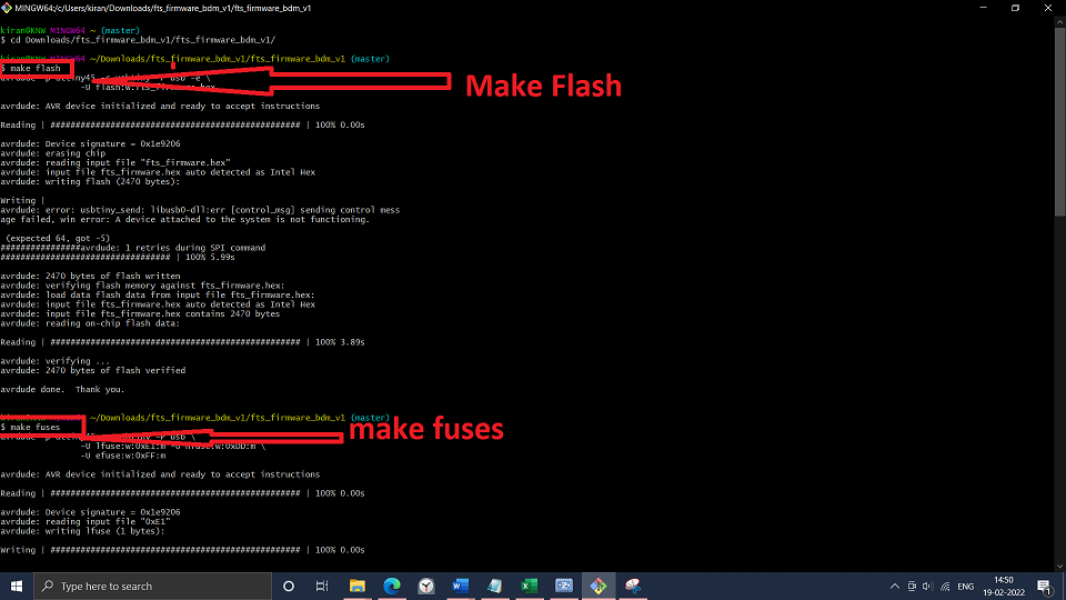
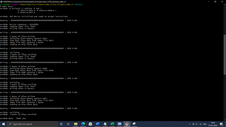
Run the make fuses command. This will set up all of the fuses except the one that disables the reset pin.
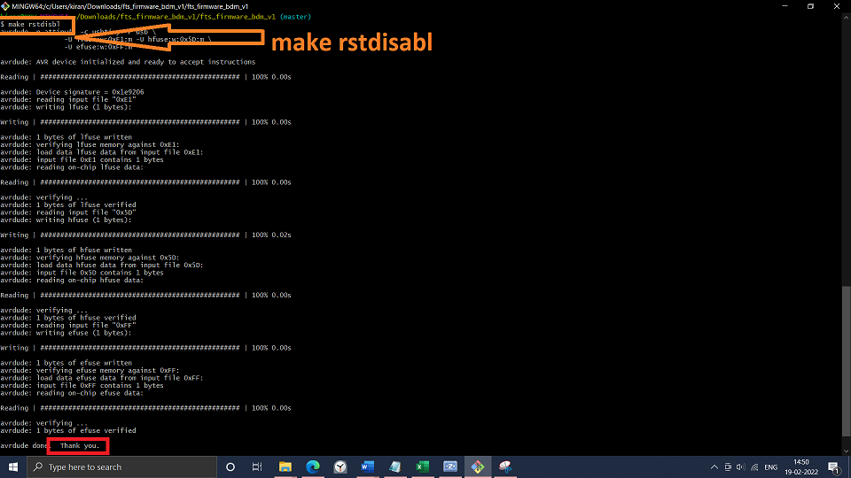
Run make rstdisbl. This does the same thing as the make fuses command, but this time it's going to include that reset disable bit as well. You should see some progress bars, and with that, avrdude will never be able to talk to this chip again through the ISP header.
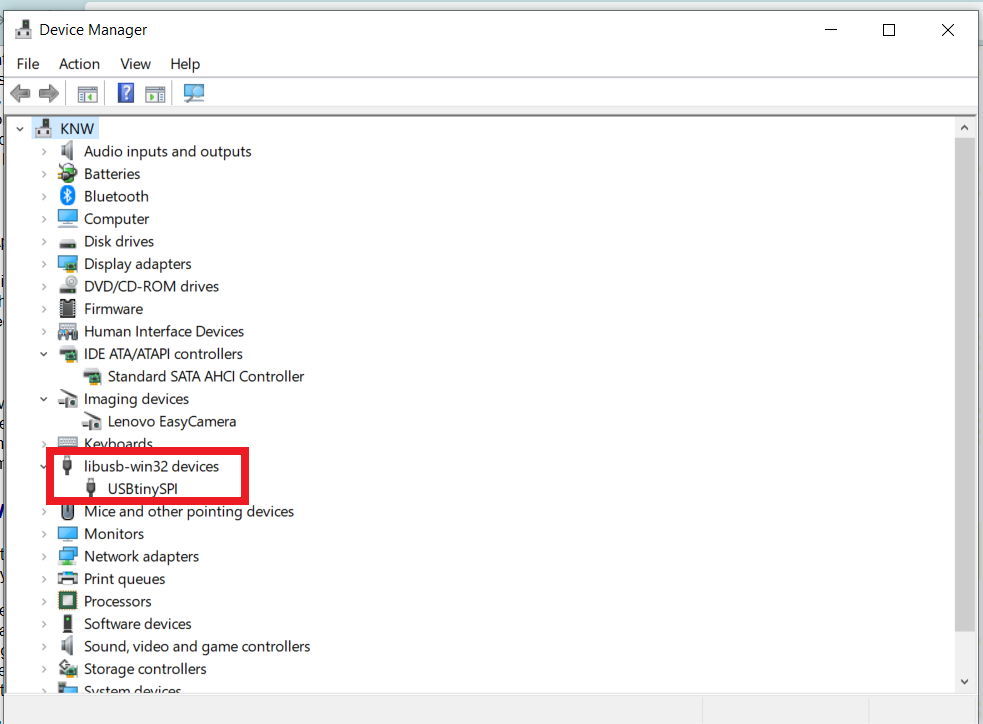
Windows lists USB devices in Device Manager (Start → Control Panel → System → Device Manager), and I found USBTiny- means my Programmer is successfully installed and ready to program other microcontrollers.