6. Electronics Design
This page documents my Week 6 workflow based on the Electronics Design assignment: from project setup in KiCad to schematic, PCB layout, manufacturing outputs, and production-oriented updates.
Group assignment page: Chaihuo Lab Week 6 Group Assignment
Assignment checklist
- Linked to the group assignment page and reflected on group work
- Used EDA tool (KiCad) for schematic and board layout
- Documented electronics design workflow
- Exported production files (Gerber)
- Included design files
Self Reflection (Based on Group Work)
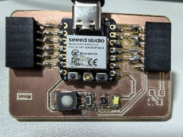
In the Week 6 group assignment, we practiced using a multimeter and an oscilloscope to measure real circuits instead of only drawing them in KiCad. Measuring 5.00 V between GND and VCC on an ESP32 made the power net on my schematic feel concrete — a labeled rail is not the same as a verified supply at the board edge.
Measuring current in series (about 2.78 mA between a GPIO pin and GND) helped me understand why current paths matter when I route traces and choose resistor values. The meter has to break the circuit to read current, which is a useful reminder that every return path through GND is part of the design, not an afterthought.
On the oscilloscope, we captured the servo PWM waveform while the ESP32 moved the horn to 90°, 0°, and −90°. Seeing pulse width change on the screen connected firmware timing to physical motion. That made me think more carefully about header placement, signal routing, and ground reference when I laid out my Hello World board — debug access and clean grounds are easier to design in than to fix after milling.
My main takeaway is that schematic design and bench measurement support each other. KiCad tells me what the circuit should do; the multimeter and scope confirm whether the built board actually behaves that way. I will carry that habit into Week 8 production and later embedded weeks: design with test points in mind, verify power first, then check signals before assuming a layout problem is a software bug.
How to Complete Week 6
- Collect and organize links to your circuit source files and PCB layout outputs. HelloWorldWeek6-F_Cu.gbr HelloWorldWeek6-Edge_Cut.gbr
- Install and launch KiCad.
- Download and unzip the Fab Academy KiCad library.
- Use this command if needed:
git clone https://gitlab.fabcloud.org/pub/libraries/electronics/kicad.git.
- Create a new KiCad project.
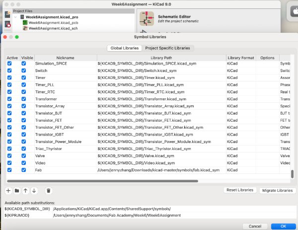
- Import the symbol library in
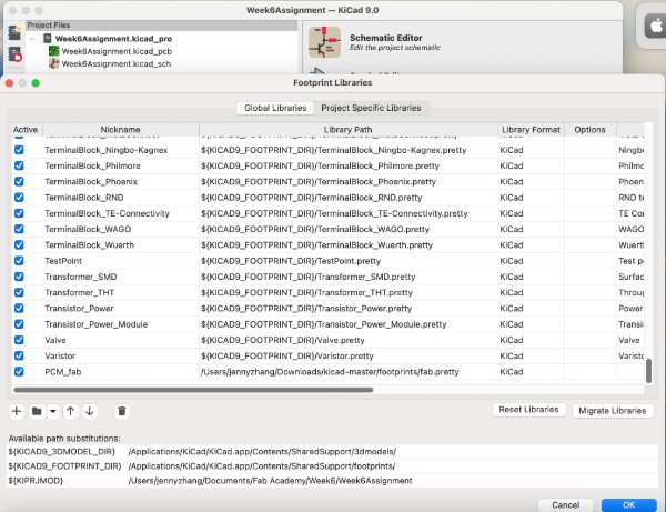
Manage Symbol Libraries. - Import the footprint library in
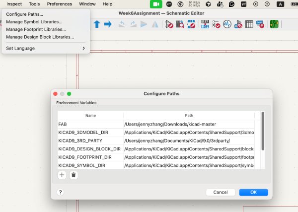
Manage Footprint Libraries. - Set the library path in
Settings -> Configure Pathsso 3D models load correctly.
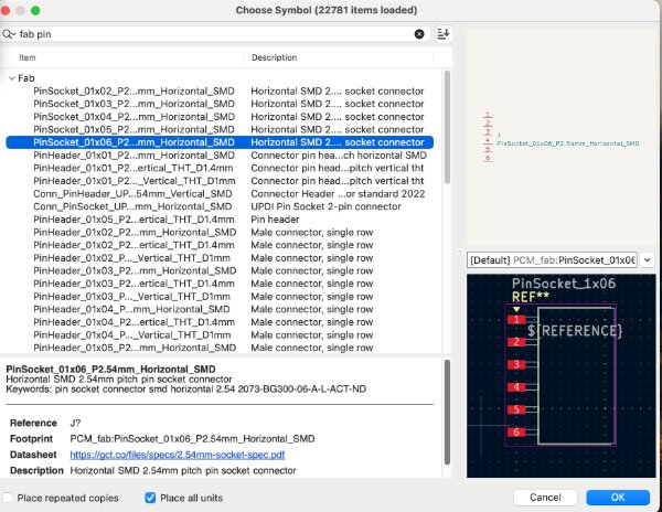
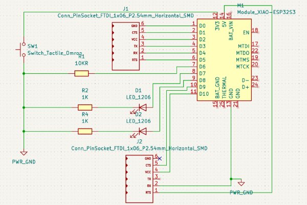
- Place the main MCU.
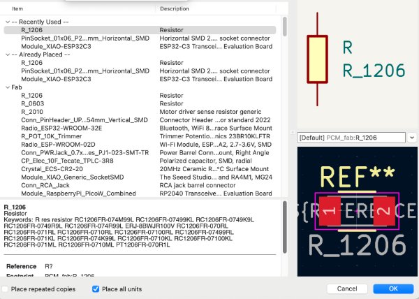
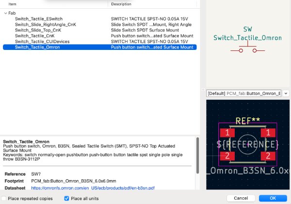
- Add required components such as an LED, switch/button, headers, and resistors.
- Create the switch-resistor logic (for example, a pull-down resistor setup).
- Complete wiring and verify all net connections.
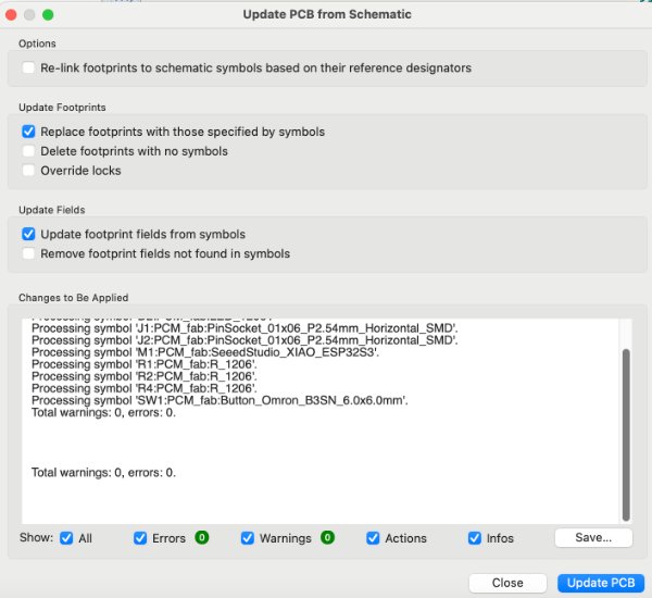
- Use
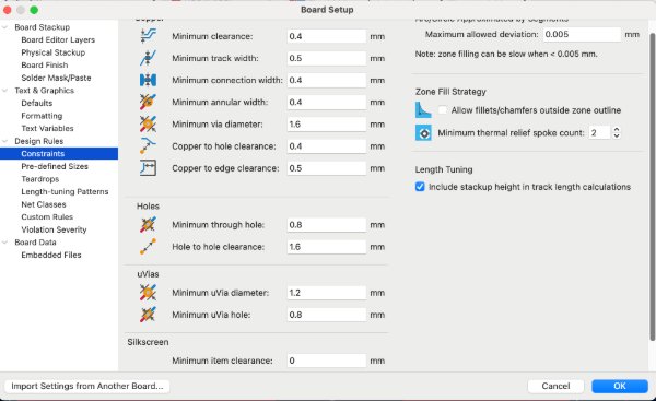
Update Schematic to PCBto transfer the design to board view. - Set board rules (trace width, clearance, and related constraints).
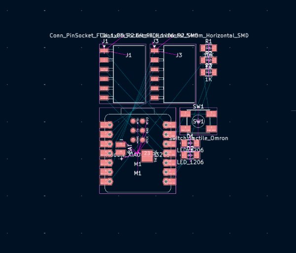
- Place components and route traces.
- Draw the board outline on
Edge.Cuts. - Run DRC and resolve all reported issues.
- Review the board in 3D Viewer.
- Round board corners on
Edge.Cuts(for example, 3 mm radius). - Add teardrops via
Edit -> Add Teardrops. - Add a copper fill on
F.Cuusing netGND, then refill zones withb. - Keep safe spacing between copper zones and signal traces.
- Export Gerber files from KiCad.
- Convert
F_Cu.gbrandEdge_Cut.gbrto PNG using Gerber2Png. - Import PNG files into Mods to generate CNC toolpaths / G-code (trace and cut).
- Publish final screenshots and output files in your documentation.