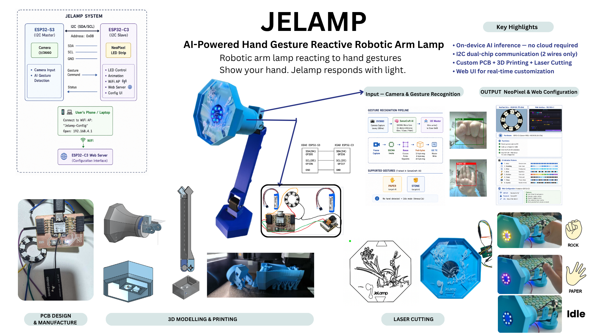
Final Project: JeLamp — AI Gesture Reactive Desk Lamp
JeLamp is an AI-powered desk lamp that recognizes hand gestures through an onboard camera, runs inference on-device with SenseCraft AI, and responds with coordinated NeoPixel lighting. The arm is a fixed mechanical structure — three Feetech STS3215 housings (Week 12) serve as joint connectors only, not as actuators. The project combines custom PCB fabrication (Week 8 design), 3D-printed mechanics, laser-cut lamp panels, dual-MCU I2C communication, and a Wi-Fi web interface into one desk companion.

JeLamp system overview — PCB, mechanical fabrication, AI pipeline, and final assembly.
Documentation Sections
Project Overview
JeLamp combines a static Luxo-inspired arm structure, dual ESP32 controllers, and on-device gesture AI into one desk lamp. The mechanical structure is modeled in Onshape and fabricated through 3D printing and laser cutting; STS3215 servo bodies define joint geometry but are not wired for motion. Electronics reuse the Week 8 custom PCB (XIAO ESP32-C3) as the lighting slave, paired with an ESP32-S3 Sense module for camera vision and I2C master control.
An onboard camera runs a SenseCraft AI hand-gesture model on the ESP32-S3 Sense; detected gestures (paper / stone) are sent over I2C to the ESP32-C3 board, which drives a NeoPixel ring with matching colors. A Wi-Fi web interface allows manual LED control when gesture mode is not active.
Key Features
- On-device AI: SenseCraft pretrained gesture model — no cloud required.
- Dual-MCU I2C architecture: ESP32-S3 master (vision) + ESP32-C3 slave (lighting + web UI).
- Custom PCB: Week 8 Hello World board design, milled and populated for the lamp head electronics.
- Fabrication: 3D-printed arm structure, laser-cut acrylic lamp panel, hand-soldered PCB.
- Interactive lighting: Paper (布) → blue wave; Stone (石头) → red pulse; idle → warm breathe.
Who is it for?
- Desk workers and students: A smart lamp that responds to hand gestures for quick mood or mode changes.
- Tech and design enthusiasts: A complete maker project combining ML, embedded systems, and mechanical design.
- Makers and educators: Fully documented workflow from KiCad PCB to SenseCraft AI deployment.
Research and References
Apple’s ELEGNT research on expressive and functional movement for non-anthropomorphic robots informed the lamp’s form language and interaction design. In the final build, expression comes through NeoPixel colour and pattern — the arm itself stays fixed.
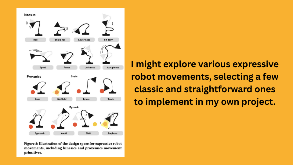
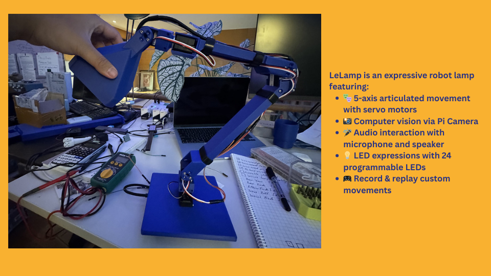
I also studied open-source projects such as LeLamp and other Luxo-inspired robotic lamps. These references helped with joint layout, STS3215 mounting geometry, and reproducible maker workflows — even though my final lamp does not actuate its joints.
Modeling and Prototyping
Early prototyping referenced open-source projects such as LeLamp for joint layout and connector sizing. The final mechanical arm was modeled parametrically in Onshape starting in Week 2, with integration planning and concept sketches documented in Week 16.
JeLamp Concept Rendering
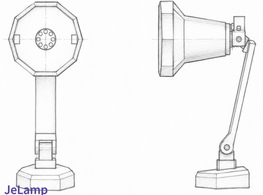
Concept sketch from Week 16 — arm segments, lamp head, and base layout.
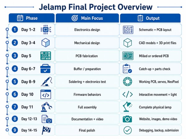
Integration overview — mechanical, electronics, AI, and assembly timeline.
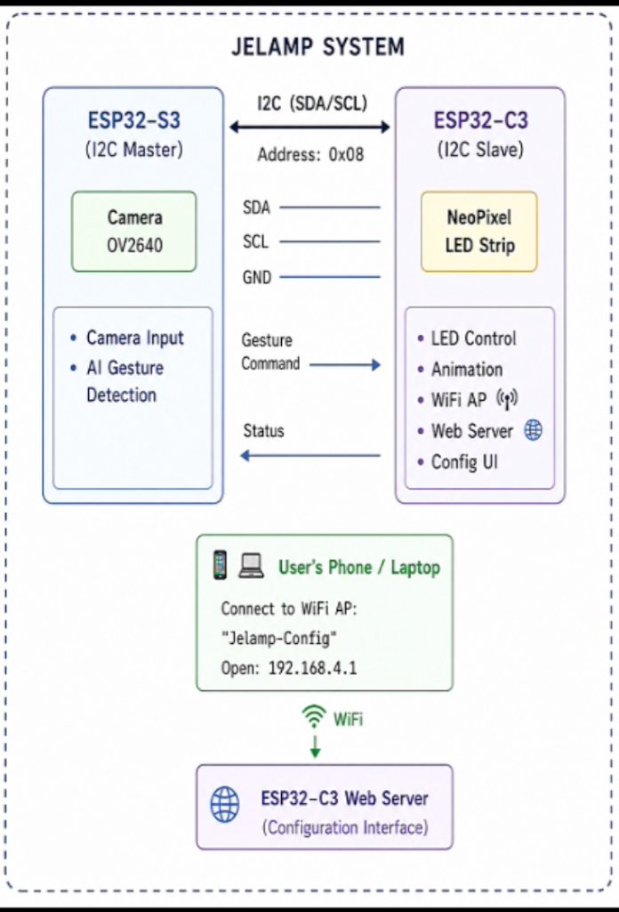
JeLamp system block diagram — ESP32-S3 (AI + I2C master) and ESP32-C3 (NeoPixel + web UI).
Hero Video
One-minute overview of JeLamp: fabrication steps, gesture recognition demo, and final operation. Full presentation materials are also on Week 20.
presentation.mp4 (~1 min) — fabrication, gesture demo, and final operation.
Summary slide: presentation.png.
Final System Architecture
JeLamp uses a dual-microcontroller architecture. The ESP32-S3 Sense (master) handles camera input, on-device AI inference, and I2C command output. The ESP32-C3 on the Week 8 custom PCB (slave) drives the NeoPixel ring, hosts a Wi-Fi access point, and serves the configuration web UI.
                    +---------------------------+
                    |   User (hand gesture)     |
                    +-------------+-------------+
                                  |
                                  v
+------------------------------------------------------------------+
|  MASTER: XIAO ESP32-S3 Sense                                     |
|  - OV2640 camera + SenseCraft AI gesture model                     |
|  - I2C Master  SDA(D4)/GPIO5, SCL(D5)/GPIO6                       |
+----------------------------+-------------------------------------+
                             | I2C @ 100 kHz, GND + SDA + SCL
                             v
+------------------------------------------------------------------+
|  SLAVE: XIAO ESP32-C3 on Week 8 custom PCB                       |
|  - I2C Slave @ 0x08  SDA(D4)/GPIO6, SCL(D5)/GPIO7               |
|  - NeoPixel x8 on D3 + Wi-Fi config web UI @ 192.168.4.1         |
+------------------------------------------------------------------+

Gesture mapping (SenseCraft model):
  target=0 Paper (bu)   -> blue wave
  target=1 Stone (shitou) -> red pulse
  no detection (2 s)    -> warm idle breathe
- Input: OV2640 camera → SenseCraft AI pretrained hand-gesture model (on-device, no cloud).
- Communication: I2C between S3 master and C3 slave; Wi-Fi HTTP for manual control.
- Output: NeoPixel ring color and pattern (gesture-mapped lighting only — arm is static).
- Mechanical: 3D-printed arm segments + laser-cut hexagonal lamp head panel.
Detailed integration planning: Week 16 System Integration.
1. PCB Design & Manufacture
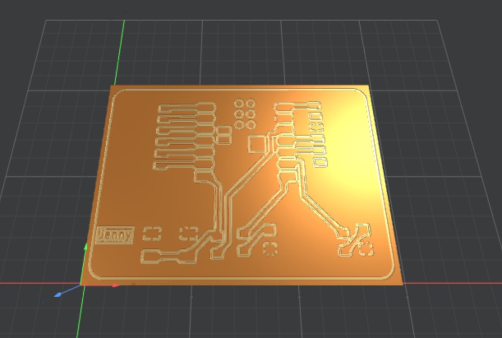
JeLamp's custom electronics board reuses the Week 8 Hello World design — a KiCad carrier for the XIAO ESP32-C3 with breakout headers, button, and LEDs. I designed the schematic and PCB layout in Week 6, milled it on the KEXU CNC in Week 8, then revised and validated the populated board. In the final project this board acts as the I2C slave and NeoPixel driver in the lamp head.
Full step-by-step PCB documentation (schematic, layout, milling, soldering, testing) lives on the Week 8 assignment page. Below is the process summary for the final project.
Step 1 — Schematic Design (KiCad, Week 6)
- Create project
HelloworldNewin KiCad 8 with Fab Academy library (fab.kicad_sym,fab.pretty). - Place XIAO ESP32-C3 module (U1), two 1×6 pin headers (J1, J2), tactile switch (SW1), two 1206 LEDs (D1, D2), and current-limiting resistors.
- Add 10 kΩ pull-up on the button input net (revised after first test).
- Run ERC until zero errors; annotate components and assign SMD footprints (1206 resistors, SMA diode if used).
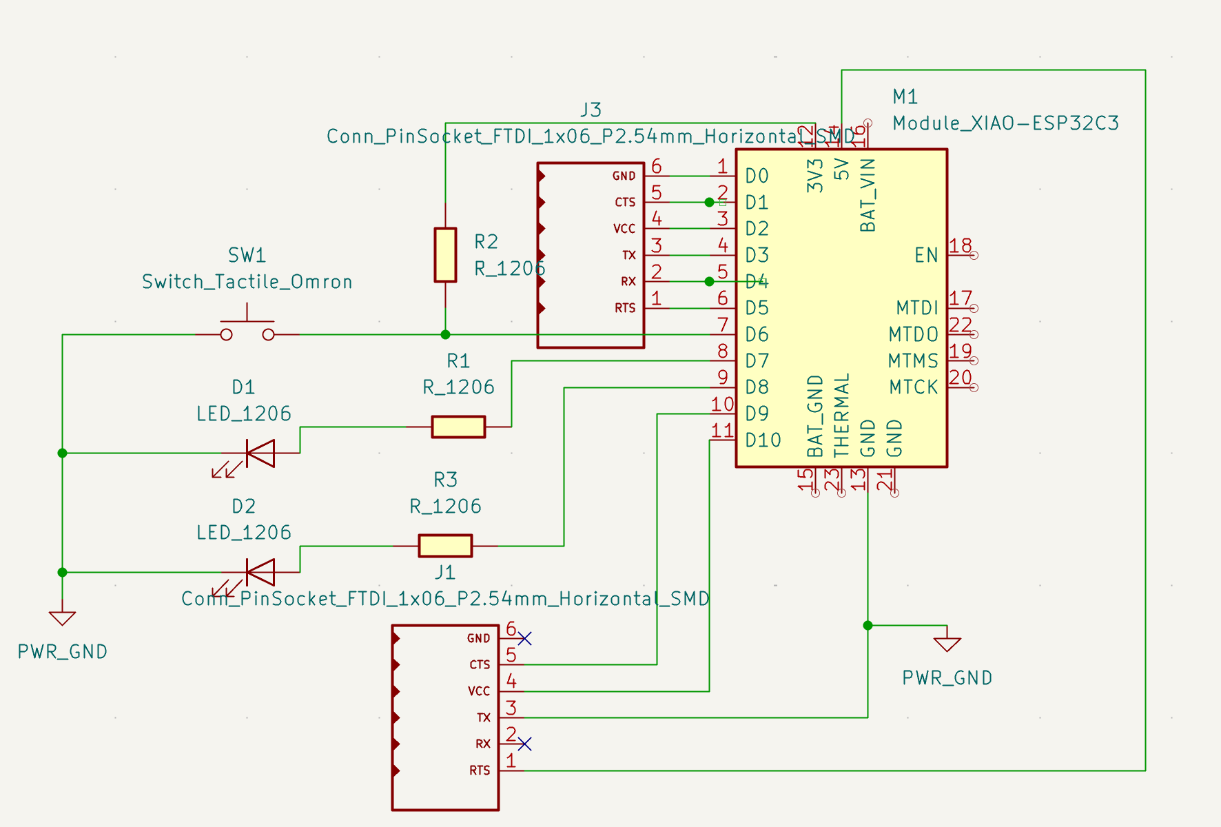
Revised schematic with pull-up resistor on button input — from Week 8.
Step 2 — PCB Layout
- Update PCB from schematic; set board outline to match XIAO module + header breakout area.
- Set design rules for in-house milling: ≥ 0.38 mm trace/space, ≥ 0.5 mm preferred for power paths.
- Place XIAO with USB-C edge accessible; route signal traces at 0.4 mm, keep ground pour on copper layer.
- Add silkscreen labels for pin functions and board title.
- Run DRC; export Gerbers (
F.Cu,Edge.Cuts) for milling.
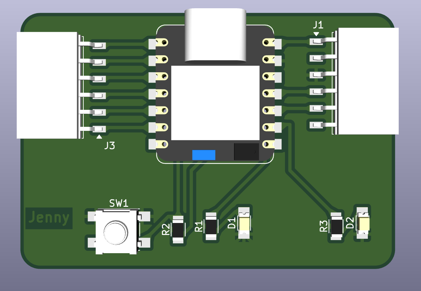
KiCad 3D view — XIAO footprint, pin headers, and breakout traces.
Top-layer layout with ground pour and silkscreen labels.
Step 3 — G-code Generation (Mods CE)

Gerber2PNG — white traces on black background.
Mods CE — V-bit trace pass and outline cut presets.
3D toolpath preview before cutting — verify isolation paths and outline.
- Convert Gerber to PNG via Gerber2PNG — white traces on black background.
- Open Mods CE in Chrome → program → Open Program.
- Load
traces_toplayer_0.png; set 40° #502 V-bit preset; calculate and save trace G-code. - Reload outline PNG; use 1.5 mm ball-end mill preset; calculate and save outline G-code.
- Simulate 3D preview before cutting — verify no stray dots or missing isolation paths.
Step 4 — CNC Milling (KEXU)
- Secure 1.6 mm FR-4 copper-clad on sacrificial plate with double-sided tape.
- Install V-bit; set X/Y origin at front-left corner; Z zero with paper-drag test.
- Run trace G-code at 14,000 rpm, 4 mm/s feed, 0.23 mm cut depth.
- Swap to ball-end mill; re-zero Z; run outline pass to cut board free.
- Deburr with sandpaper; wash board with soap and water before soldering.
Trace isolation pass on the KEXU CNC — from Week 8.
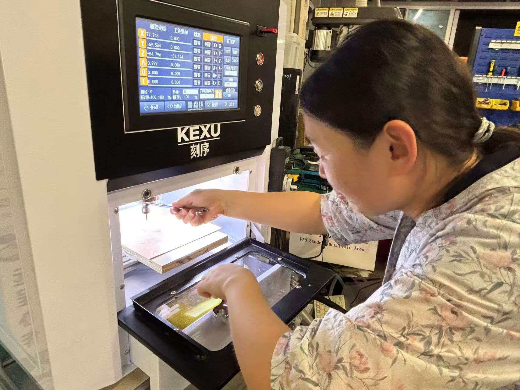
Board secured on sacrificial plate; V-bit trace pass.
Milled board after deburring — ready for component placement.
Step 5 — Soldering & Board Test
- Solder SMD passives first (resistors, LEDs, switch), then pin headers, then XIAO module last.
- Inspect joints under magnification; check no bridges on castellated pads.
- Multimeter: no short between 5 V and GND.
- Flash HelloWorldWeek8.ino — button on D7 toggles LEDs on D8/D9.
- After pull-up fix, order revised board from JLCPCB for reliable production units used in JeLamp.
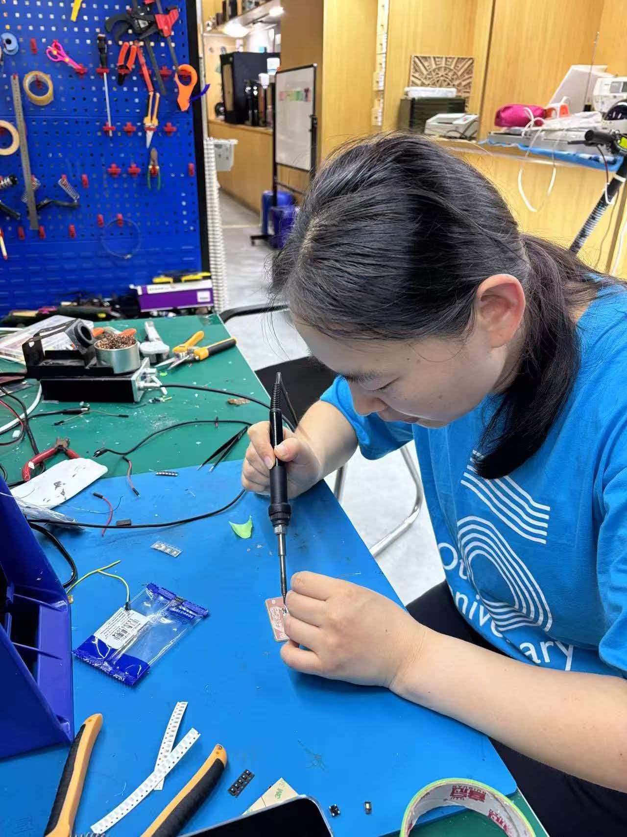
Hand-soldering passives and pin headers before mounting the XIAO module.
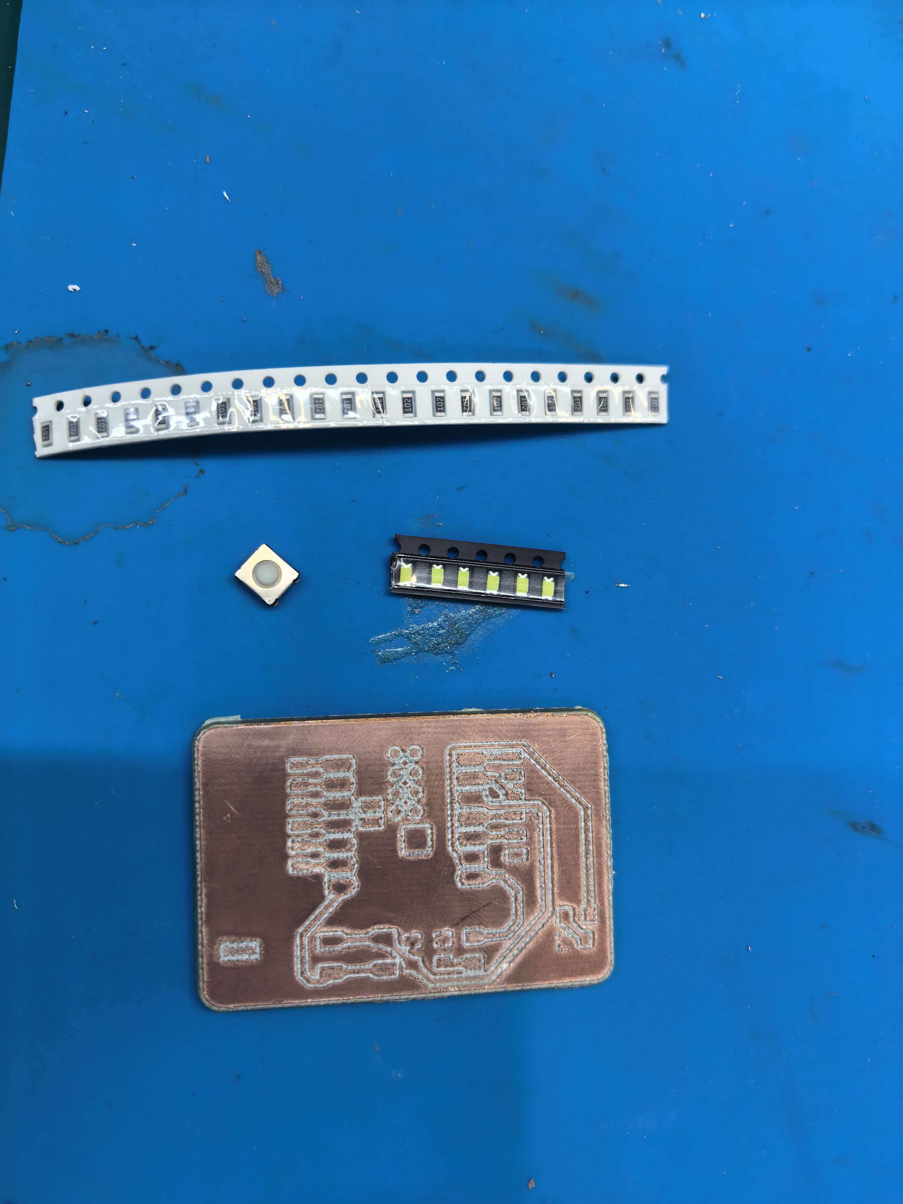
Completed solder joints — XIAO module and headers mounted.
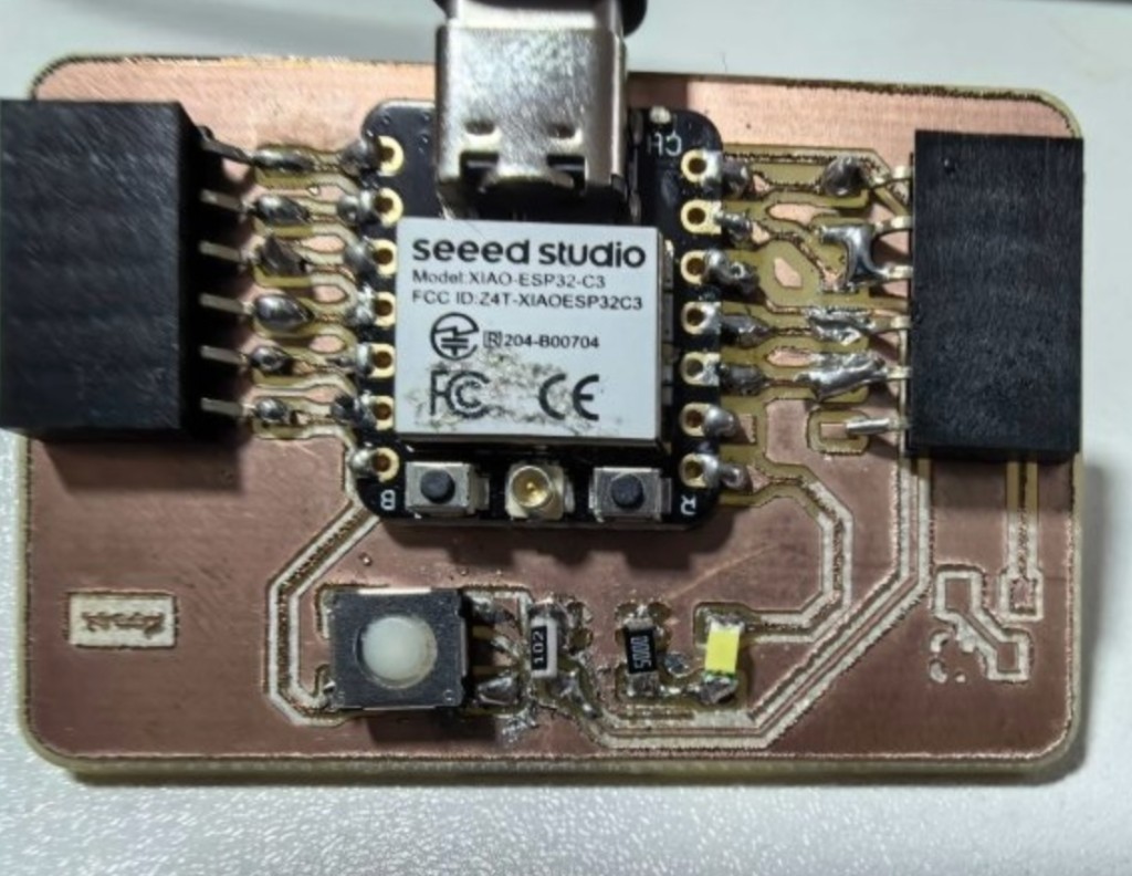
Populated carrier board running HelloWorldWeek8 test firmware.
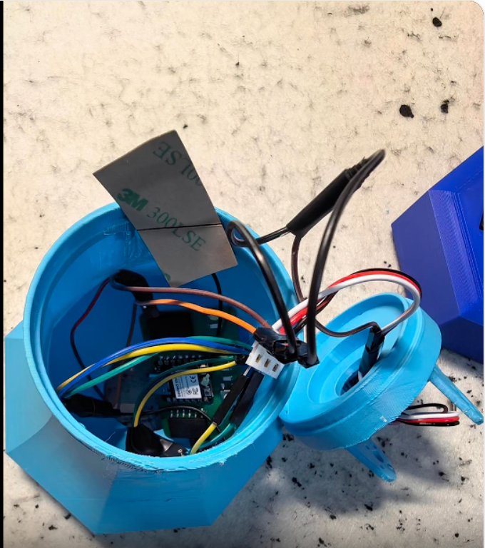
Final project wiring: In JeLamp assembly the ESP32-C3 board connects to the NeoPixel ring and receives gesture commands from the ESP32-S3 over I2C (SDA/SCL + common GND). See Week 8 for pin maps and test firmware.
2. 3D Modelling & Printing
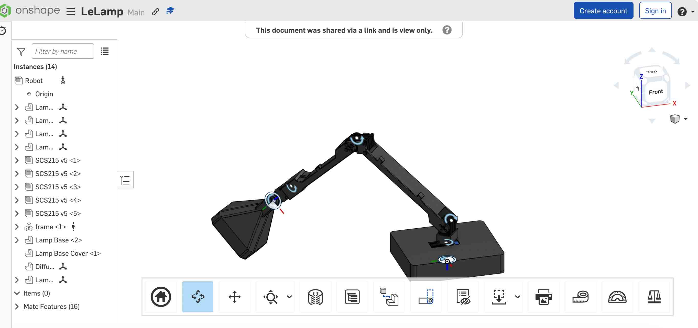
The JeLamp mechanical structure is a fixed Luxo-style arm designed in Onshape. Three Feetech STS3215 bodies (Week 12) are used as structural joint connectors — horns and housings lock arm segments together, but the servos are not powered or programmed to move. Each custom part is built around the imported STS3215 STEP model; joint positions come from Assembly → Mate connectors, not fixed sketch numbers. Parts are FDM-printed in PLA at Chaihuo Fab Lab. Live model: Robotic Arm document.
Step 1 — CAD Design (Onshape)
1. Import STS3215 motor model as reference
- Create a new Onshape document (
Jelamp); set workspace units to mm (File → Units). - Download or import the Feetech STS3215 STEP model into the document (appears as
SCS215 v5in the parts list). - Insert the servo into an Assembly tab — do not redesign the motor body; treat it as a fixed reference volume.
- Add a Mate connector at the output horn center (Z along shaft axis) — this becomes the anchor for every joint above it.
- Measure horn bolt circle, body width, and shaft height from the imported model before sketching any custom plastic.
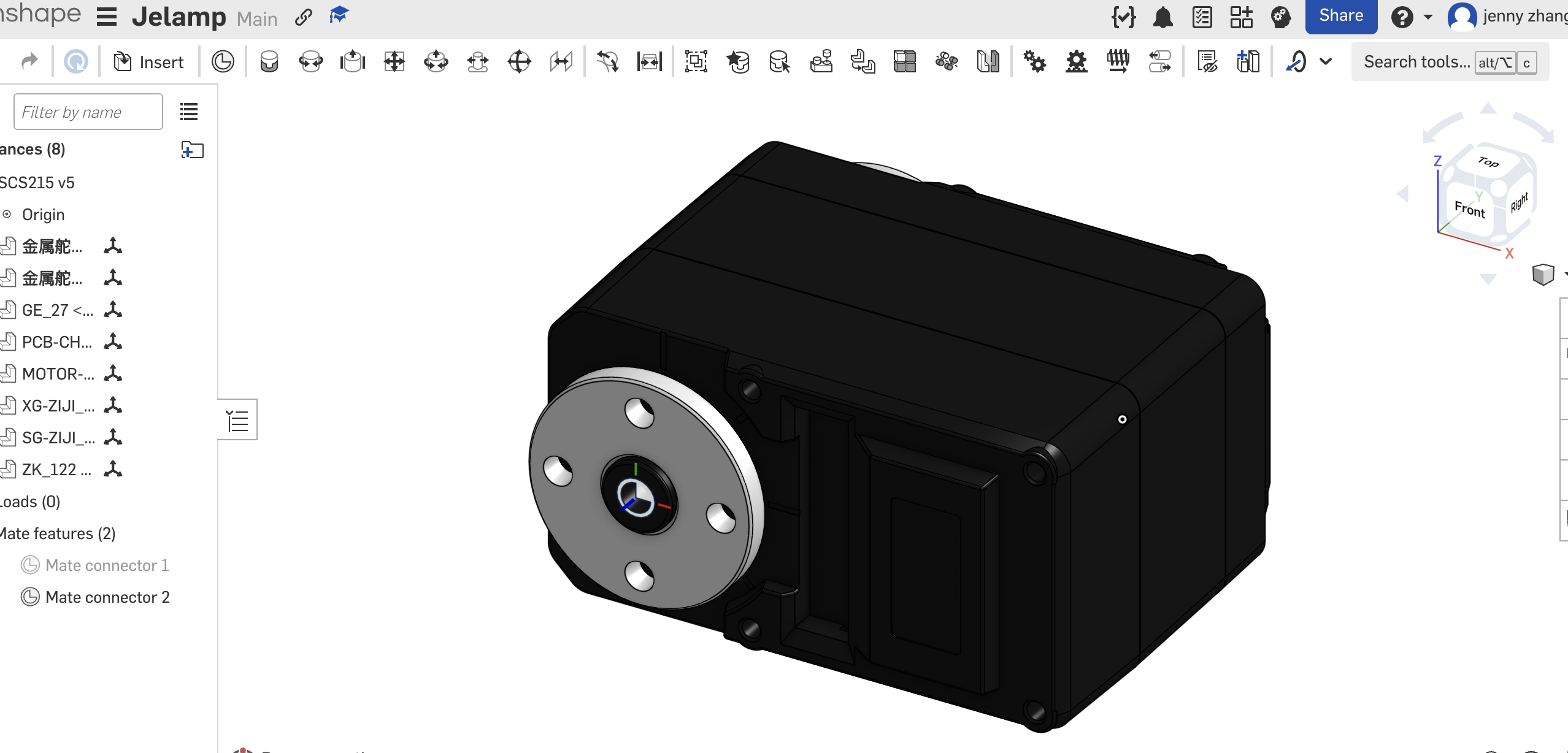
Imported STS3215 reference in Assembly — mate connectors at horn centers (SCS215 v5 in instances list).
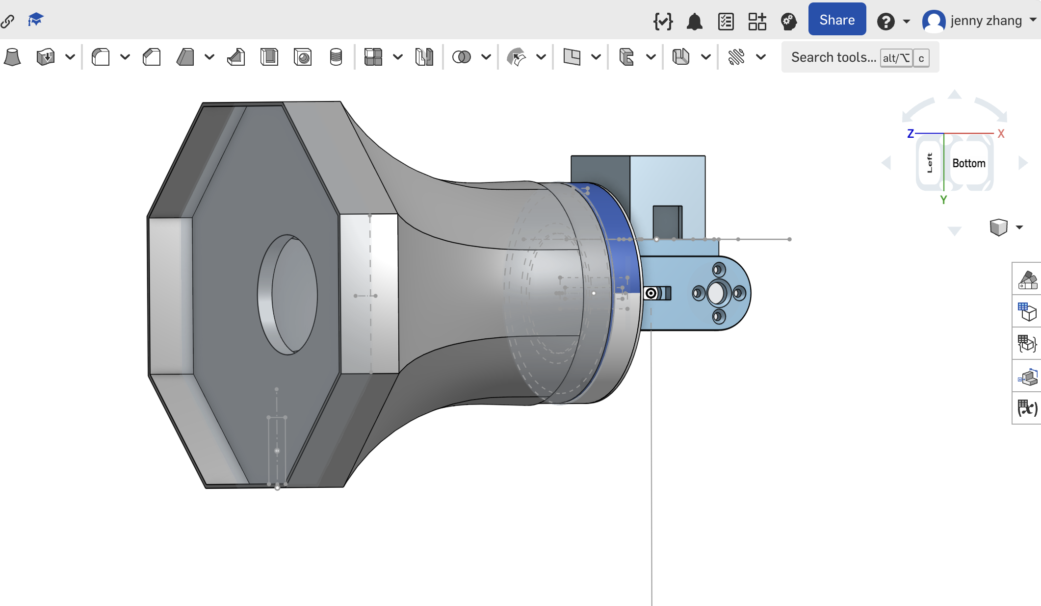
2. Lamp base — Assembly mates define placement
- Switch to a new Part Studio for the base; sketch the footprint on the Top plane using projected servo edges from the assembly.
- Extrude / revolve the base shell with a central pocket that clears the STS3215 body and exposes the mounting ears.
- Model horn-adaptor features (circular boss + 4× M2 holes) that match the mate connector orientation from Step 1.
- Return to Assembly; insert the base part and Fasten it to the bottom servo mate connector — adjust offset until the base sits flush on the desk plane.
- Add cable pass-through slots for I2C wiring before exporting STL.
Base joint geometry — circular pocket sized to the STS3215 horn adaptor; fillets added before print.
3. Lamp arm connections — sized to STS3215 interface
- For each joint, create a separate part (lower arm, upper arm, neck) with its own mate connector at the STS3215 horn center.
- Sketch horn-adaptor profiles by projecting the STS3215 top face — match the 4-hole pattern and splined bore clearance.
- Extrude arm tubes with Up to vertex / Up to face so link length updates when mate offsets change in Assembly.
- Mate each arm segment to the next STS3215 instance in Assembly; verify clearance and that the fixed pose matches the intended lamp silhouette.
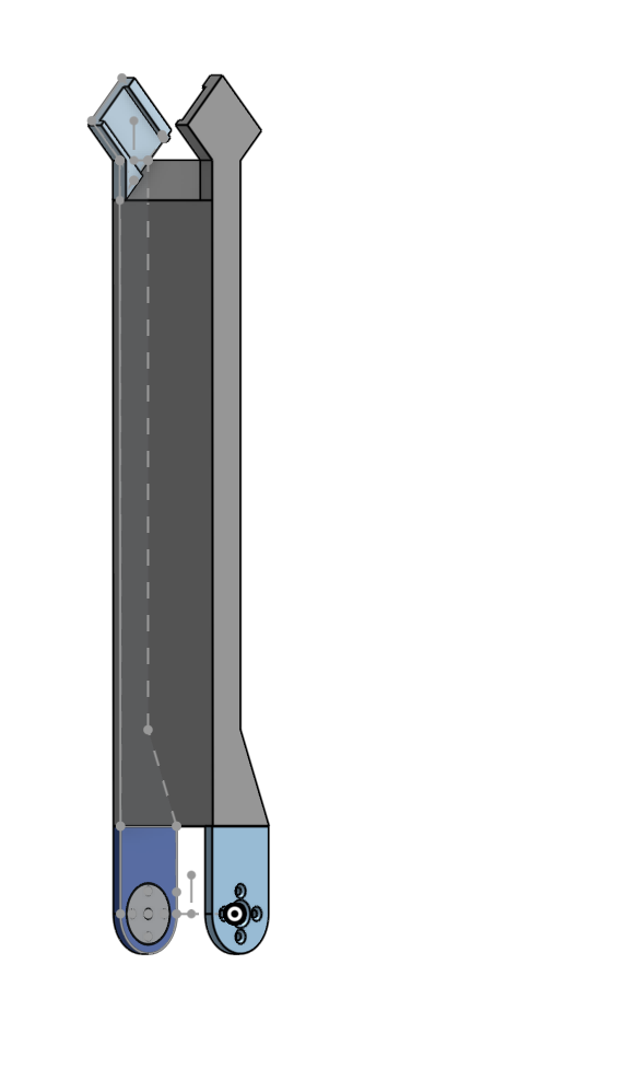
Arm coupling — extrude-to-vertex link tied to mate connector position, not a fixed length value.
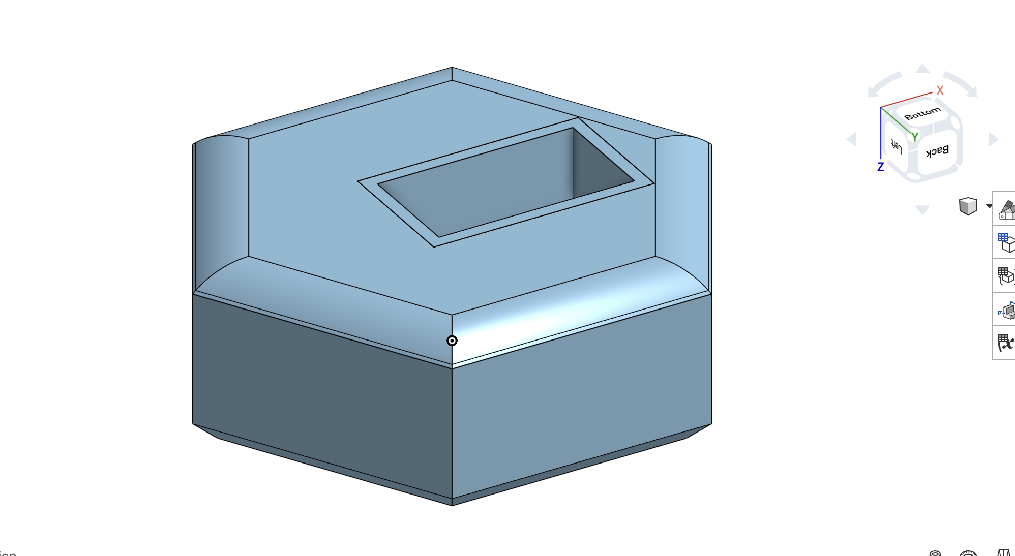
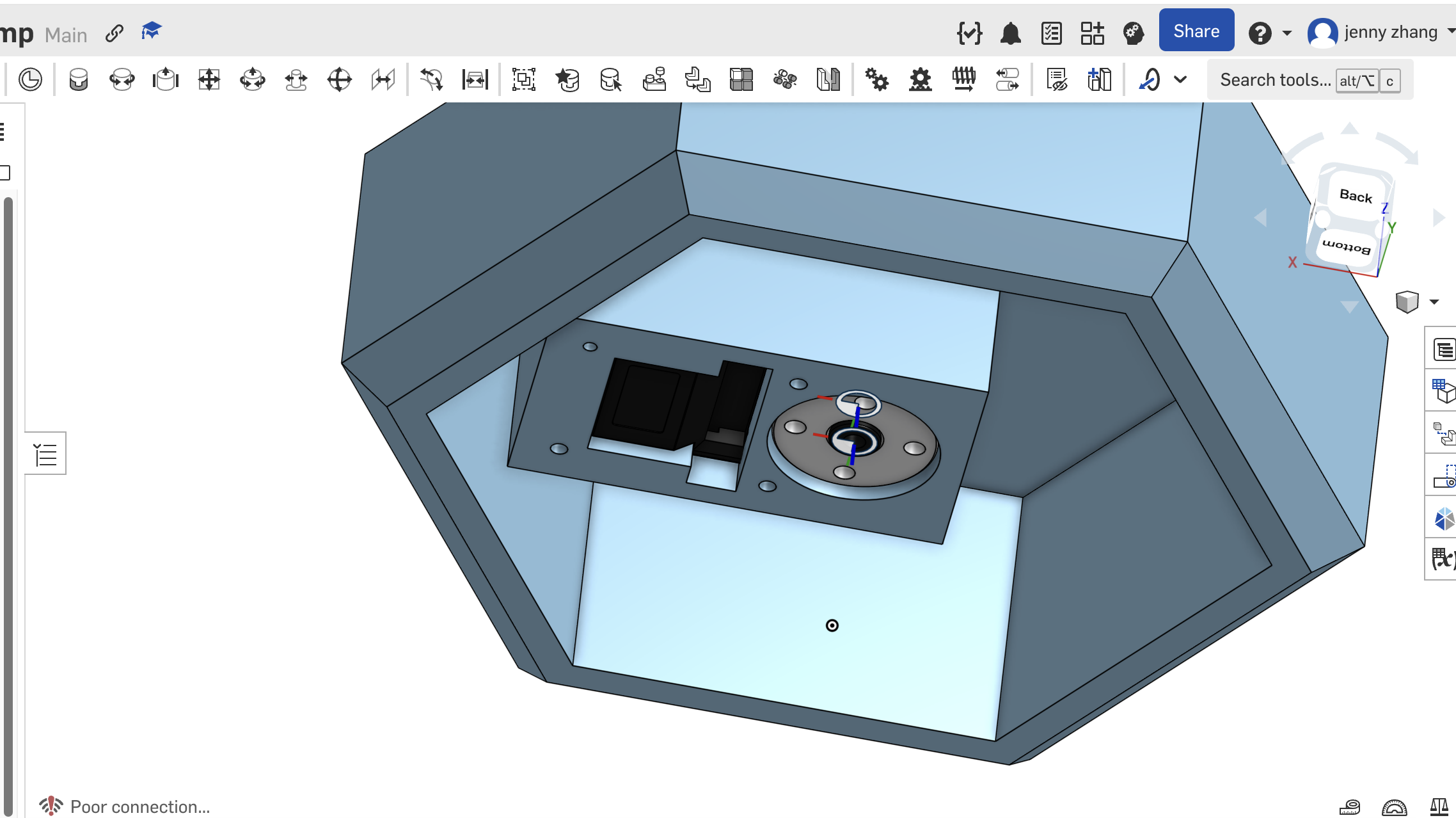
4. Lamp head — measure electronics, then set dimensions
- Measure physical parts with calipers: XIAO ESP32-S3 Sense module, Week 8 / carrier PCB, NeoPixel ring OD, and camera lens field-of-view cone.
- Import or sketch simplified envelope solids for each board; place them inside a head Assembly to find required cavity length, width, and height.
- Design the hex shell with internal shelf for the PCB, ring recess for NeoPixels, and a front opening aligned to the OV2640 camera.
- Add a sloped face or light pipe gap for the acrylic laser-cut panel; mate the head to the top STS3215 via horn adaptor + mate connector.
- Run interference check in Assembly; adjust wall thickness until all boards fit with ≥ 1 mm clearance, then export STLs.
Step 2 — Slicing & Print Settings
- Import STLs into PrusaSlicer / Bambu Studio; orient parts to minimize overhangs on servo pockets.
- Layer height 0.2 mm; infill 20–30% for structural parts, 15% for decorative shell.
- Enable supports only where bridging exceeds ~ 10 mm (e.g. under lamp head overhang).
- Print brim or raft on tall narrow parts to reduce warping on the heat bed.
- Group small parts on one plate only if they share material and layer time.
Step 3 — FDM Printing
- Load PLA filament (blue for arm segments; white optional for lamp shade).
- Level bed and verify first-layer adhesion before long prints.
- Print base and arm segments sequentially; monitor first layers for warping.
- Remove support structures carefully; deburr servo pocket edges with a small file.
- Dry-fit STS3215 connectors and laser-cut panel before final assembly.
3. Laser Cutting — Design & Cutting Process
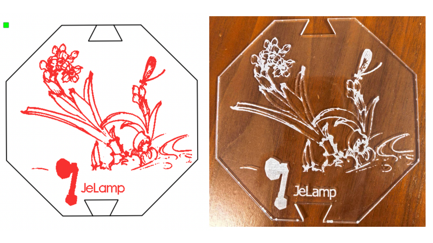
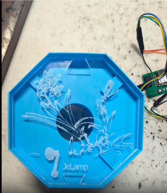
The lamp head front panel is a hexagonal piece with floral etching and the JeLamp logo, cut from translucent blue acrylic on the Thunder Laser Nova 51. Laser cutting skills from Week 3 were applied to kerf compensation and power/speed tuning.
Step 1 — Vector Design
- Create hex outline in an Onshape sketch (derived from lamp head opening dimension) or Inkscape; size to press-fit into the 3D-printed recess.
- Add decorative floral pattern as vector paths for raster engraving (not cut-through).
- Place "Jelamp" logo text at bottom of panel; convert text to paths.
- Assign cut layer (hex perimeter) vs engrave layer (decorative lines) in separate colors for the laser job.
- Export as SVG or DXF; verify stroke widths and closed paths.
Vector layout with cut vs engrave layers — same workflow as Week 3.
Step 2 — Laser Job Setup
- Material: 3 mm translucent blue acrylic (verify no PVC / chlorine content).
- Focus lens to material surface; enable fume extraction before starting.
- Cut settings (reference from Week 3 group tests): adjust power/speed for clean edge on acrylic.
- Engrave settings: lower power, higher speed — test on scrap first to avoid melting fine lines.
- Apply kerf offset (~ 0.15 mm per side) so panel press-fits into 3D-printed recess.
Step 3 — Cutting & Post-processing
- Secure acrylic sheet flat on honeycomb bed; run cut pass for hex perimeter.
- Run engrave pass for floral pattern and logo.
- Remove protective film; peel off any smoke residue with mild soap and water.
- Test press-fit into lamp head; lightly sand edges if too tight.
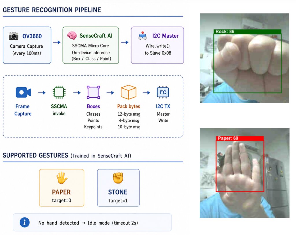
4. AI Model & Gesture Recognition (SenseCraft AI)
JeLamp recognizes paper and stone hand gestures using a pretrained SenseCraft AI model on the XIAO ESP32-S3 Sense. Inference runs on-device (no cloud). Results are packed and sent over I2C to the ESP32-C3 slave, which drives the NeoPixel ring.
Architecture — Dual Board + I2C
Dual-board architecture: ESP32-S3 (Master) → I2C → ESP32-C3 (Slave)

Board 1 — ESP32-S3 Sense (base)
  • OV2640 camera + SenseCraft AI / SSCMA_Micro_Core inference
  • I2C master: sends Box / Class packets to slave 0x08

Board 2 — ESP32-C3 (Week 8 PCB, lamp head)
  • I2C slave @ 0x08
  • NeoPixel ring on D3
  • Optional Wi-Fi web UI (Week 15)
Step 1 — I2C Wiring
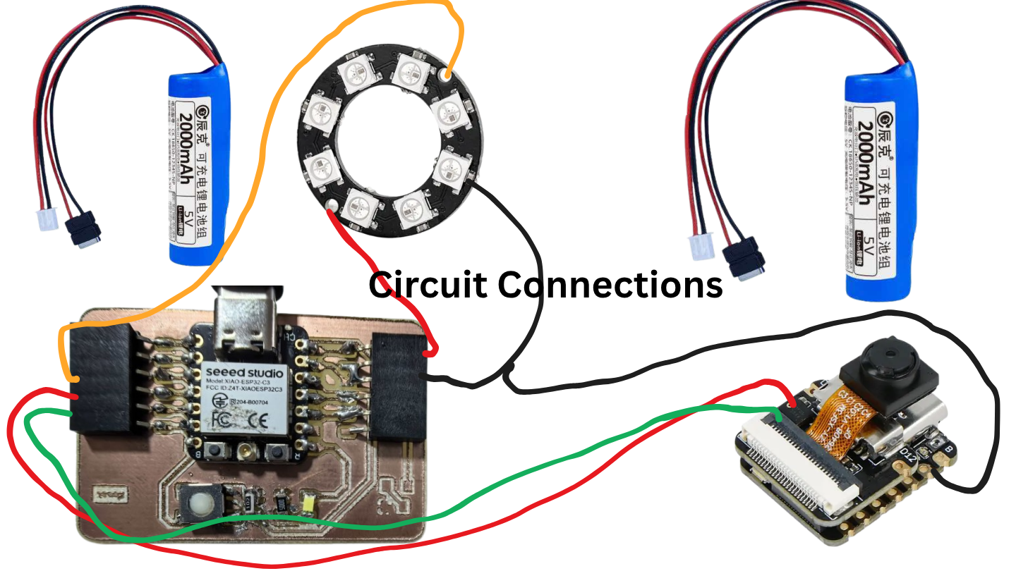
ESP32-S3 (Master) → I2C → ESP32-C3 (Slave)

  XIAO ESP32-S3          XIAO ESP32-C3
  ┌──────────┐          ┌──────────┐
  │ SDA(D4)  ├──────────┤ SDA(D4)  │
  │ GPIO5    │          │ GPIO6    │
  │          │          │          │
  │ SCL(D5)  ├──────────┤ SCL(D5)  │
  │ GPIO6    │          │ GPIO7    │
  │          │          │          │
  │ GND      ├──────────┤ GND      │
  └──────────┘          └──────────┘
| Signal | ESP32-S3 (Master) | ESP32-C3 (Slave) |
|---|---|---|
| SDA | D4 / GPIO5 (Arduino pin 5) | D4 / GPIO6 |
| SCL | D5 / GPIO6 (Arduino pin 6) | D5 / GPIO7 |
| GND | GND | GND (common) |
| Bus speed | 100 kHz (Wire.setClock(100000) on master) | |
| Slave address | 0x08 | |
3-wire cable (GND, SDA, SCL) through hollow arm from base to lamp head.
Step 2 — SenseCraft AI Model Deployment
- Open SenseCraft AI Model Assistant.
- Select board: XIAO ESP32-S3 Sense.
- Choose the pretrained hand gesture model (paper / stone — 布 / 石头).
- Flash the model firmware via USB-C; confirm Serial output shows class labels.
- Install the SSCMA_Micro_Core library in Arduino IDE (bundled with SenseCraft export).
- Merge custom I2C send code (JeLamp_S3_Master.ino) with the inference loop.
SenseCraft AI Model Assistant — paper / stone gesture classes on ESP32-S3 Sense.
Step 3 — I2C Packet Protocol
Master packs SenseCraft inference into byte arrays. First byte = packet type:
| Type | Len | Format |
|---|---|---|
0x01 Box | 12 B | [0x01][x][y][w][h][score][target] — coords ×100, big-endian int16 |
0x02 Class | 4 B | [0x02][score_hi][score_lo][target] |
0x03 Point | 10 B | [0x03][x][y][z][score][target] |
0xFF Perf | 7 B | [0xFF][preprocess][inference][postprocess] ms timings |
SenseCraft class targets → NeoPixel (C3 slave):
| target | Gesture | Default effect |
|---|---|---|
| 0 | Paper (布 bu) | Blue wave |
| 1 | Stone (石头 shitou) | Red pulse |
| −1 | No detection (2 s timeout) | Warm idle breathe |
Step 4 — Source Code
All files in public/files/final-project/. Download links below — full source, not snippets.
| File | Board | Description |
|---|---|---|
| JeLamp_S3_Master.ino | ESP32-S3 Sense | SenseCraft AI + camera + sendBox / sendClass / sendPoint / sendPerf |
| JeLamp_C3_Slave.ino | ESP32-C3 | Basic I2C slave — paper wave / stone pulse / idle breathe |
| JeLamp_C3_Slave_Web.ino | ESP32-C3 | Advanced — web UI for color + pattern + speed; requires types.h |
| types.h | ESP32-C3 | PatternType, GestureConfig, IdleConfig — place next to Web .ino |
Board 1 — ESP32-S3 Master (excerpt)
#include <SSCMA_Micro_Core.h>
#include <Wire.h>

#define C3_SLAVE_ADDR 0x08
#define I2C_SDA       5    // ESP32-S3 D4 / GPIO5
#define I2C_SCL       6    // ESP32-S3 D5 / GPIO6

void sendClass(const SSCMAMicroCore::Class& cls) {
    uint8_t buf[4];
    buf[0] = 0x02;
    int16_t score = (int16_t)(cls.score * 100);
    buf[1] = (score >> 8) & 0xFF;
    buf[2] = score & 0xFF;
    buf[3] = (int8_t)cls.target;
    Wire.beginTransmission(C3_SLAVE_ADDR);
    Wire.write(buf, 4);
    Wire.endTransmission();
}

void setup() {
    Wire.begin(I2C_SDA, I2C_SCL);
    Wire.setClock(100000);
    capture.begin(SSCMAMicroCore::VideoCapture::DefaultCameraConfigXIAOS3);
    instance.begin(SSCMAMicroCore::Config::DefaultConfig);
}

void loop() {
    auto frame = capture.getManagedFrame();
    instance.invoke(frame);
    for (const auto& cls : instance.getClasses()) sendClass(cls);
    delay(100);
}
Board 2 — ESP32-C3 Slave (excerpt)
#define I2C_SLAVE_ADDR  0x08
#define NEOPIXEL_PIN    D3
#define NUM_PIXELS      8

Wire.begin(I2C_SLAVE_ADDR);
Wire.onReceive(onReceive);

// MSG_CLASS: buf[1..2]=score, buf[3]=target
// target 0 -> effectPaper (blue wave)
// target 1 -> effectStone (red pulse)
// timeout 2 s -> effectIdle (warm breathe)
Upload settings
| Board | Sketch | Libraries |
|---|---|---|
| XIAO ESP32-S3 Sense | JeLamp_S3_Master.ino |
SSCMA_Micro_Core (SenseCraft AI) |
| XIAO ESP32-C3 | JeLamp_C3_Slave.ino or JeLamp_C3_Slave_Web.ino + types.h |
Adafruit NeoPixel · Web version also: WiFi, WebServer, DNSServer, Preferences |
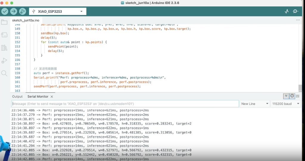
Step 5 — On-device Validation
- Flash C3 slave first; confirm boot animation (blue / red sweep) then idle breathe.
- Connect I2C; flash S3 master; Serial @ 115200 — watch
Class: target=… score=…. - Show paper (target 0) → blue wave; show stone (target 1) → red pulse.
- Remove hand for 2 s → idle warm breathe returns.
- Web version: connect to AP
RPS-XXXX, openhttp://192.168.4.1, tune colors/patterns.
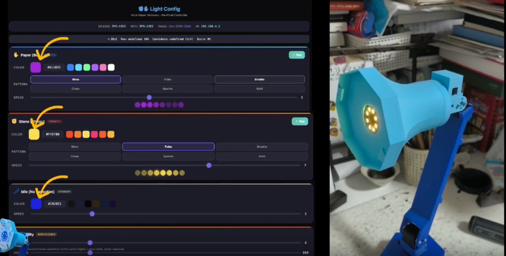
5. Web Interface & Output (Advanced C3 Firmware)
The advanced slave firmware JeLamp_C3_Slave_Web.ino
adds a Wi-Fi access point and browser config UI. SSID is auto-generated from MAC
(e.g. RPS-A1B2); password rps-xx-xx-xx. IP: 192.168.4.1.
Web UI Features
- Per-gesture color picker + hex input + preset swatches (Paper / Stone / Idle).
- Pattern selection: Wave, Pulse, Breathe, Chase, Sparkle, Solid.
- Speed slider (1–10) per gesture; live LED preview bar.
- Save to flash (Preferences), reset defaults, test flash button.
- Captive portal — phone auto-opens config page when joining AP.
Requires types.h in the same sketch folder. Design spec: Week 15.
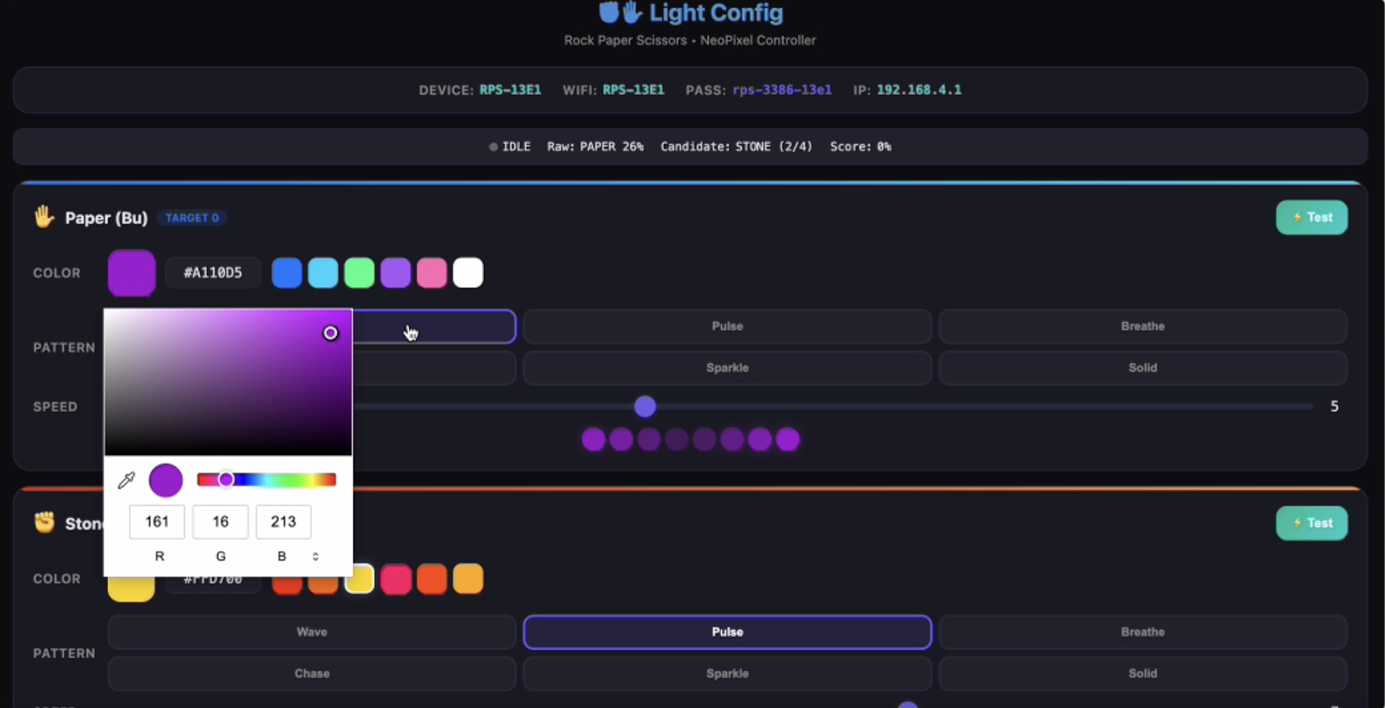
Browser config UI — per-gesture color, pattern, and speed — from Week 15.
6. Assembly & System Testing
After each subsystem is validated independently, all parts are assembled into the complete JeLamp. The assembly order below minimizes rework if a cable or joint needs adjustment.
Step 1 — Pre-assembly Bench Tests
- Flash C3 slave (
JeLamp_C3_Slave.inoor Web version); confirm boot sweep + idle breathe. - Flash S3 master; connect I2C; verify
Class: target=0/1on Serial. - Show paper → blue wave; show stone → red pulse on NeoPixel strip.
Step 2 — Mechanical Assembly
- Install STS3215 housings into 3D-printed base and arm segments as fixed connectors; attach horns and lock segments at the designed pose (no power to servos).
- Route flexible silicone I2C wires through hollow arm; leave 15–20 mm slack at the head joint.
- Mount ESP32-S3 Sense in base with camera facing user; expose USB-C for reprogramming.
- Mount ESP32-C3 PCB and NeoPixel ring inside lamp head; press-fit laser-cut acrylic panel.
- Secure lamp head to upper arm; tighten M3 screws without pinching cables.
- Add base cover; attach ballast weight if needed for stability.
Step 3 — Integrated System Test
- Power on from single 5 V / 7.4 V supply; confirm both MCUs boot.
- Show paper (target 0) → verify blue wave NeoPixel response.
- Show stone (target 1) → verify red pulse response.
- Remove hand 2 s → idle warm breathe returns.
- Web version: join
RPS-XXXXWi-Fi; openhttp://192.168.4.1; test color/pattern save. - Confirm fixed arm pose is stable and I2C cable has no strain at joints.
- Record hero video (
presentation.mp4) showing fabrication, gesture demo, and lighting response.
Full measured results and failure notes are documented in Results & What Didn't Work below.
7. Results & What Didn't Work
During integrated testing I recorded actual numbers against the success criteria from Week 18. The table below replaces the original target checklist with measured outcomes. Evidence comes from Serial Monitor logs, the integrated demo in presentation.mp4, and the bench / assembly photos on this page.
Measured Results vs. Targets
Test setup: XIAO ESP32-S3 Sense + Week 8 ESP32-C3 PCB, SenseCraft pretrained
paper/stone model, JeLamp_S3_Master.ino + JeLamp_C3_Slave_Web.ino,
5 V supply, camera 40–50 cm from hand. For gesture accuracy I ran 20 attempts per gesture
(40 total) in each lighting/background condition below, holding each pose ~1 s.
| Metric | Target (Week 18) | Measured | Verdict |
|---|---|---|---|
| Gesture accuracy (desk lighting) | > 80% correct classification | 85% in the primary test condition — plain wall behind the hand, desk lamp on (~500 lux), no clutter in frame (34 / 40 correct). Accuracy dropped sharply when background or lighting changed; see breakdown table below. Serial confidence in the best condition: 72–86%; with desk clutter in frame, scores fell to 28–43% (see bench photo below). | Pass |
Gesture accuracy by background and lighting
The SenseCraft pretrained model was not retrained for my desk — it assumes a relatively clean view of the hand. Background objects and lighting direction changed results more than gesture type.
Takeaway: the > 80% target is met only when I control background and add a desk lamp pointed at my hand. In everyday use at a messy desk or near a bright window, accuracy falls to roughly 45–70%. For the final demo I cleared the camera view and used the plain-wall setup; the anti-flicker filter (Problem 1 below) reduced false triggers in borderline conditions.
Bench test Serial output — box scores 28–43% with desk clutter in frame (backlit / cluttered condition).
Integrated test — plain-wall setup with desk lamp; web UI anti-flicker at 4 frames / 800 ms hold; lamp head showing stone (yellow pulse) response.
What Broke and How I Fixed It
Problem 1 — Background and lighting destroyed accuracy; LED flickered between paper and stone.
With a plain wall and desk lamp, Serial confidence stayed at 72–86%. But with a cluttered desk,
backlit window, or dim room, scores dropped to 28–55% and the model flipped between
target=0 and target=1 several times per second — the NeoPixel cycled
colours even when my hand did not change.
Fix: For the demo I cleared the camera view (plain wall, no keyboard in frame), added a desk lamp aimed at my hand (~500 lux), and enabled anti-flicker in the web UI firmware — require 4 consecutive frames above threshold with an 800 ms hold before switching patterns. That raised accuracy from ~47% (backlit) and ~65% (cluttered desk) to 85% in the controlled setup, but the filter also slows response in borderline lighting.
Problem 2 — I2C packets lost after routing through the printed arm. On the first
assembled build, the NeoPixel sometimes stayed on idle breathe even though S3 Serial printed
Class: target=0/1. C3 Serial showed gaps in received packets.
Fix: Added 4.7 kΩ pull-up resistors on SDA and SCL at the S3 master
(Week 16 plan), switched to twisted-pair silicone wire, kept the I2C harness away from the 5 V power
line, and left 15–20 mm slack at the head joint. Confirmed with
Wire.setClock(100000) — no missed updates in a 5-minute soak test after the rewire.
Project Materials
| Qty | Description | Use in Final Project | Notes |
|---|---|---|---|
| 1 | XIAO ESP32-S3 Sense | Master controller — camera, AI, I2C | OV2640 camera; SenseCraft AI; I2C master SDA(D4)/GPIO5, SCL(D5)/GPIO6. |
| 1 | Custom PCB (Week 8 Hello World design) | Slave board — NeoPixel + Wi-Fi web UI | XIAO ESP32-C3 carrier; milled in Week 8, revised via JLCPCB. |
| 3 | Feetech STS3215 servo housings | Structural joint connectors (not actuated) | Base, elbow, and head joints — horns lock arm segments; servos not wired for motion. |
| 1 | WS2812B NeoPixel strip (8 LED) | Gesture feedback on D3 | Paper → blue wave; Stone → red pulse; idle → warm breathe. |
| 1 | Translucent blue acrylic (3 mm) | Laser-cut lamp head panel | Hex shape with floral engraving and JeLamp logo. |
| 1 set | PLA filament (~300 g) | 3D-printed arm and base | Blue PLA for arm; printed at Chaihuo Fab Lab. |
| 1 | 5 V / 7.4 V power supply | System power | Single supply for both MCUs and NeoPixel ring. |
| 1 set | SMD passives, headers, wire, M3 screws | PCB assembly and cabling | 1206 resistors, pin headers, silicone wire for arm routing. |
Source Files & Resources
All original design files are archived on this website under public/files/.
Presentation
| File | Description |
|---|---|
| presentation.mp4 | Hero video — JeLamp fabrication and operation (~1 min, 1080p) |
| presentation.png | Summary slide (1920 × 1080) for Fab Academy final presentation |
| jelamp-poster.png | Project overview poster |
Electronics — Week 8 PCB (used in final project)
| File | Description |
|---|---|
| HelloworldNew.kicad_sch | KiCad schematic — XIAO ESP32-C3 carrier (revised pull-up fix) |
| HelloworldNew.kicad_pro | KiCad project file |
| HelloWorldWeek6-F_Cu.gbr | Front copper Gerber (Week 6 original, used for milling) |
| HelloWorldWeek6-Edge_Cuts.gbr | Board outline Gerber |
| traces_toplayer_0.png | Trace PNG for Mods CE milling |
| outline_toplayer_2.png | Outline PNG for Mods CE cutout |
| traces_toplayer_0.png.nc | Generated trace G-code for KEXU CNC |
| HelloWorldWeek8.ino | Board test firmware — button toggles LEDs |
| Week 8 documentation | Full PCB design, milling, soldering, and test workflow |
Mechanical — 3D & 2D design
| File | Description |
|---|---|
| JeLamp Robotic Arm — Onshape | Primary 3D model — parametric arm structure (Week 2, used for final project) |
| Week 2 documentation | Full Onshape modeling workflow with step-by-step screenshots |
| falt-pack-furniture-new.f3d | Fusion 360 flat-pack stool (Week 7 — separate assignment, not JeLamp arm) |
| Giraffe.svg | 2D vector — early lamp concept sketch |
| Week3Fab.dxf | DXF — laser cutting practice file |
| seatfinal.dxf | DXF — structural panel design |
| Week 2 · Week 5 · Week 3 | CAD, 3D printing, and laser cutting weekly documentation |
Firmware — SenseCraft AI & I2C (final project)
| File | Description |
|---|---|
| JeLamp_S3_Master.ino | ESP32-S3 — SenseCraft AI + I2C master (sendBox / sendClass / sendPoint / sendPerf) |
| JeLamp_C3_Slave.ino | ESP32-C3 — basic I2C slave + NeoPixel gesture effects |
| JeLamp_C3_Slave_Web.ino | ESP32-C3 — advanced I2C slave + web UI (color / pattern / speed config) |
| types.h | PatternType, GestureConfig, IdleConfig — use with Web slave sketch |
Firmware — weekly prototypes
| File | Description |
|---|---|
| NeoPixelUltrasonic_8LED.ino | NeoPixel output test (Week 10) |
| BoardA_Sender.ino | ESP32-S3 I2C master / wireless prototype |
| BoardB_Receiver.ino | ESP32-C3 I2C slave / NeoPixel receiver |
| application-interface-robotic-arm-lamp.md | Web UI specification (Week 15) |
| Week 16 System Integration.docx | Dual-MCU architecture and assembly plan |
| Jelamp Carrier PCB — May15.md | Extended carrier PCB design notes (reference) |
| Week 16 · Week 17 · Week 15 | System integration, AI, and web interface documentation |
Related weekly pages
| Week | Contribution to JeLamp |
|---|---|
| Week 6 | KiCad schematic and PCB layout (Hello World board) |
| Week 8 | PCB milling, soldering, board test — design reused in final project |
| Week 10 | NeoPixel output devices |
| Week 11 | I2C / networking between S3 and C3 |
| Week 15 | Wi-Fi web control interface |
| Week 16 | System integration plan and SenseCraft AI pipeline |
| Week 17 | Camera ML / gesture recognition exploration |
| Week 20 | Final presentation, BOM, and project summary |
Full project archive: gitlab.fabcloud.org · License: CC BY-NC 4.0 (Week 19)