Week 8: Electronics Production
Group Assignment
Characterize the Design Rules for your In-House PCB Production Process

Traces for Test Board
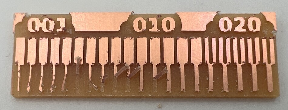
Test Board
We used a Roland SRM-20 machine that uses VPanel SRM-20 for software. The minimum width of a trace without the trace falling off was 0.13mm, though the thicker it is the more reliably it will stick. The smallest gap between traces that were successfully cut was 0.16 mm. I used a speed of 10 mm/s for both milling traces and edges. The feed speed was 4 mm/s. The cut depth for the traces was 0.1016 mm and 0.6096mm for the outline.
Submit a PCB Design to a Board House

JLCPCB Home Page, Upload Files Here
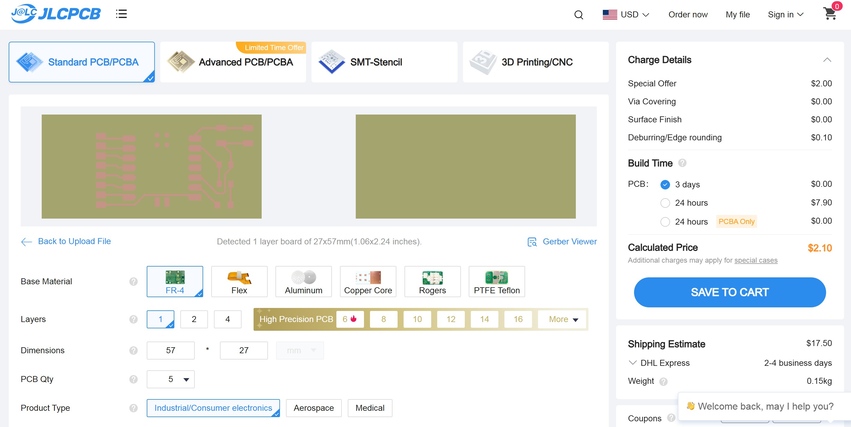
Settings & Checkout
I went through the process of submitting my board to JLCPCB up until the point you have to pay for it. I started by plotting my files the same way that I did the SVG files, I just chose Gerber instead. I then zipped all of the files together. On the JLCPCB website, I chose the “Add gerber file” button and uploaded the zip file. I was then brought to a screen with a preview of the board and lots of settings I could change. The minimum number of boards you can get is 5. I didn’t mess with the settings too much, but from what I can tell it starts you with the cheapest possible option and most other materials make it more expensive. The starting price is cheaper than I thought it would be.
Exporting Files
This section will cover how to get your board design into correctly formatted .rcd files.
KiCad
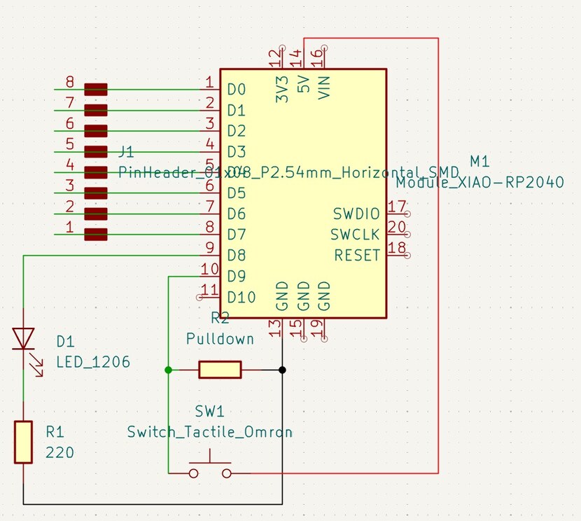
Schematic in KiCad
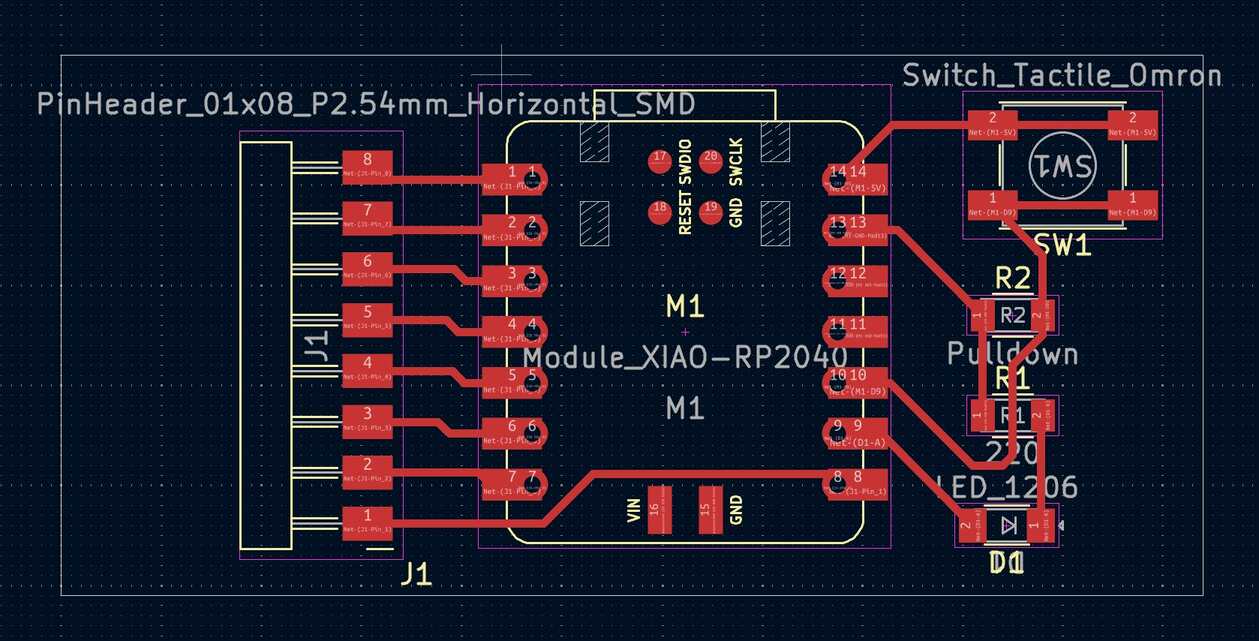
PCB Design in KiCad
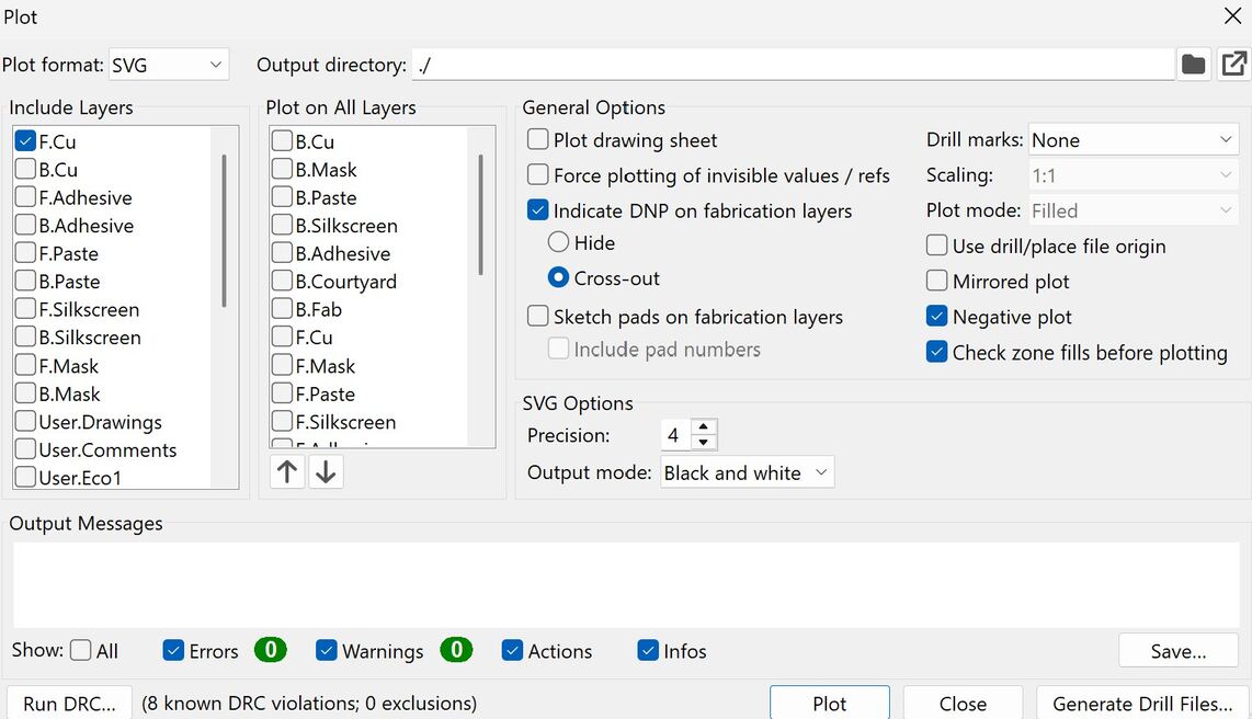
Plot Settings
I edited my week 6 design after I was given feedback from my local instructor. I needed more connectors so I added an 8 pin connector (PinHeader_01x08_P2.54mm_Horizontal_SMD) to my design. I also changed the ground to go to pin 13 instead of pin 15 because I didn’t realize pin 15 was underneath the microcontroller. I added a pulldown resistor for the button as I did not have one originally. The screenshots for the file conversion were taken before I updated the design but the steps are the same.
The first step is exporting the traces and edges as 2 different SVG files. Go to File -> Plot and choose the SVG option from the dropdown menu in the top left corner. Under Include Layers, make sure only F.Cu and Edge.Cuts are selected. On the right side, check the Negative Plot option. You can change where the files are saved in the Output Directory box at the top. When you hit plot, you will get 2 SVG files for F.Cu and Edge.Cuts respectively.
Convert to PNG

Fill in Board Shape
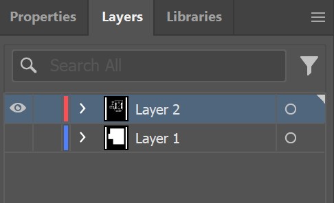
Put the Traces & Edges on Different Layers
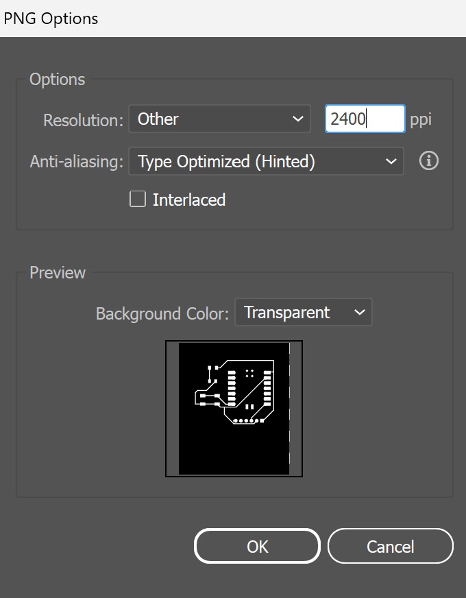
PNG Options
I used Adobe Illustrator to edit the SVG files and save them as PNGs. I started by opening the Edge.Cut file. I ungrouped the parts and filled in the outline of the board white. I then grouped the black background and white board shape back together. Next, I opened the F.Cu file and grouped together all of the pieces. I then copied the traces into the same file as the outline. Using the align tools, I centered both layers so that they were directly on top of each other. For exporting, you want to have the edges and traces in two separate PNGs. To just export one layer, you can hide the layer you don’t want to export in the layers panel. When you have only 1 layer visible, go to File -> Export -> Export As. Choose png and where you want to save it to your computer. When the PNG Options menu popped up, I set the Resolution to Other and set the ppi to 2400, and the Background Color to transparent. I did this for both the traces and the edges layers.
Create RML File
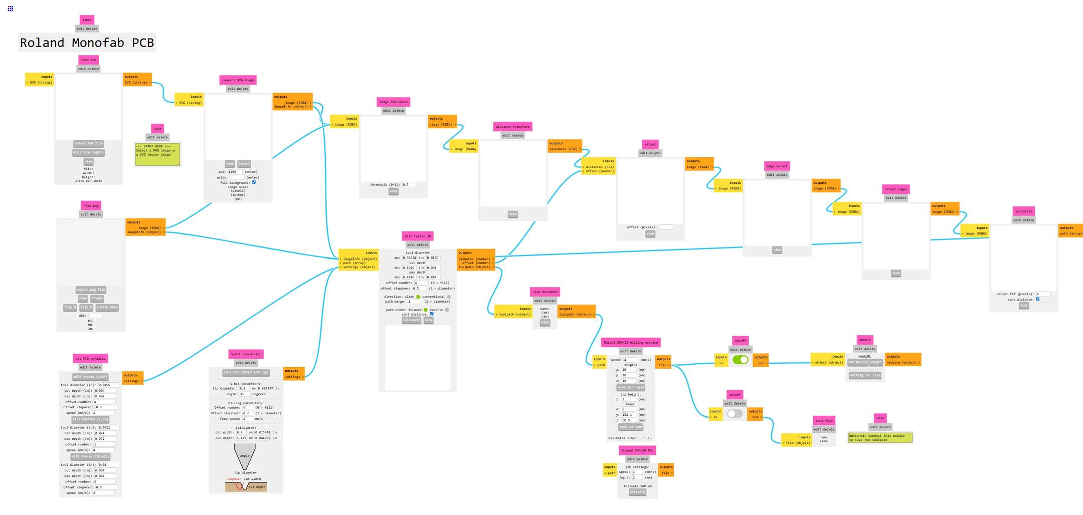
Roland Monofab PCB Program
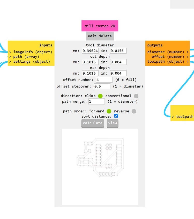
Mill Raster 2D of Traces
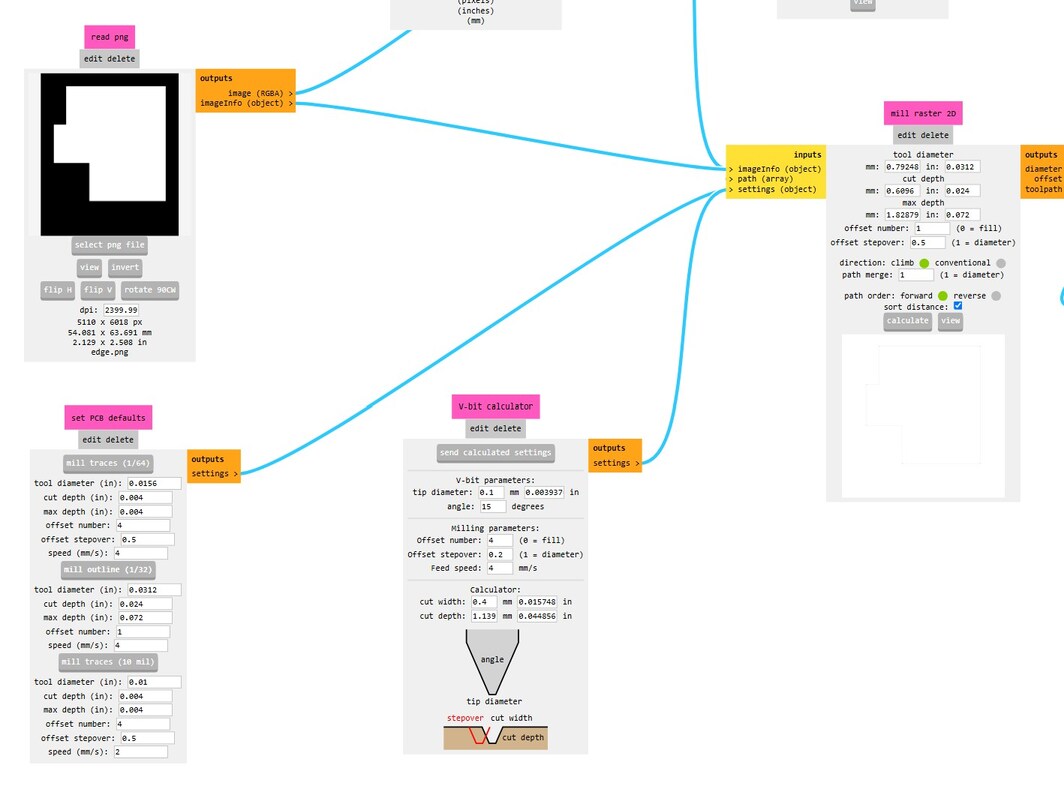
Some Settings for Edges
For this step, I used the Mods Web App. Start by right clicking and selecting Programs -> Open Programs. In this menu, I selected mill 2D PCB under SRM-20 Mill under Roland since we are using the Roland SRM-20 this week. This brings up lots of boxes with lots of connections. I started with traces PNG. In the read PNG box on the left, select “select png file” and choose your file. In the “Roland SRM-20 milling machine” box I changed the speed to 10 mm/s and the x, y, and z origins to 0. I then disabled the on/off switch that’s connected to the “WebUSB” box and enabled the on/off switch connected to the “save file” box. In the “set PCB defaults” box, I selected the “mill traces 1/64” option. Finally, in the “mill raster 2D” box, I clicked calculate. This will download your RML file and show a preview of it. It is the same process for the edges/outline PNG, I just chose the “mill traces (1/32)” option in the “set PCB defaults” box instead. I now had the correct file format for the machine’s software.
Milling the Board
We used a Roland SRM-20 to mill the circuit boards, so this section will be specific to that machine.
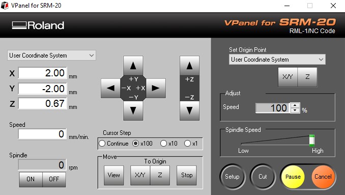
VPanel SRM-20
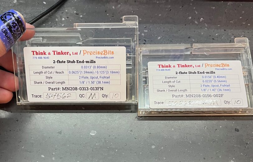
Types of End Mills Used
The first step is to attach the FR1 Copper Clad sheet to the bed of the machine. To do this, I used three strips of double sided tape horizontally across the back of the sheet. When sticking it to the bed, make sure to press down very hard to make sure the sheet stays attached. Next you need to put in the mill to cut the traces. Using the machine’s software, VPanel SRM-20, I was able to move the spindle high above the bed so that it is easier to get to. You can move the spindle on all three axes using the X+, X-, Y+, Y-, Z+, and Z- arrow buttons. To change the speed of the movement you can choose x1 which is 1/100th of a mm, x10 which is 1/10 of a mm, x100 which is 1mm, or continuous. I used a 2-flute stub 0.4mm end-mill to cut the traces. I inserted the end mill into the bottom of the spindle, at this point it doesn’t matter how much is sticking out. While holding the end mill with one hand, I inserted a hex key into a small hole near the end of the spindle and turned right to tighten it so that the mill was held in place.
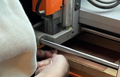
Tightening the End Mill Once on the Bed
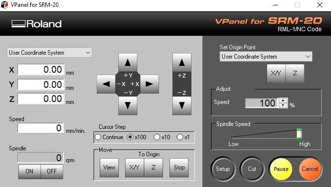
VPanel After Setting Origin
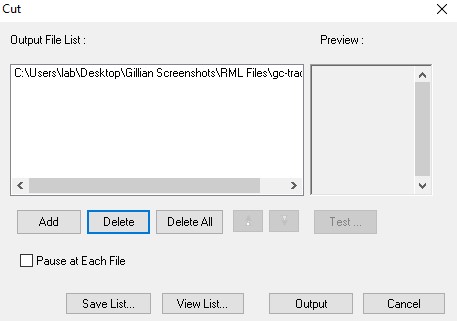
Choose The File
Next, I moved the spindle down so the end mill is just above the top right corner of the material. I then used the hex key to loosen the end mill so that it was held upright with the tip on the material but no longer attached to the spindle. I moved the spindle down so that only a little bit of the flat part of the end mill was visible. I then tightened it once again to keep it in place. With this, I could set the origin points by using the X/Y and Z buttons under the Set Origin Point dropdown box. Before starting the cut, I moved the end mill a couple millimeters above the material so that it could start spinning freely. Click the cut button in the bottom right to upload your file. If there are any files in the box, delete them using the delete button. Add your traces file by clicking Add and navigating to your RML file. Make sure the lid of the machine is closed and Output to start your cut. If there is anything concerning whilst the machine is running, you can hit the orange Cancel button on VPanel.
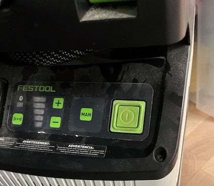
Vacuum
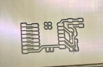
Cut Traces
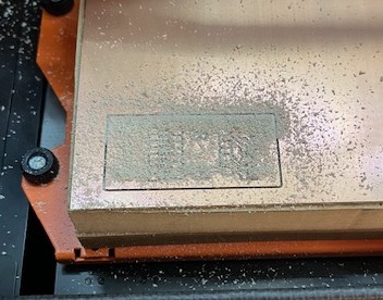
Edges Cut
Once the machine is finished, you need to clean the dust away. To use the vacuum in the lab press the big power button then press the MAN button to start the machine. I then changed it to a 0.8mm end mill. to cut out the board in the same way that I put the first end mill in. You can move the spindle to the x/y origini by pressing the X/Y button underneath To Origin. When setting the new Z origin DO NOT reset the X/Y origin, otherwise your traces won’t be lined up with the board. Once your board is finished cutting vacuum out the debris.
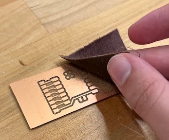
Sand the Board
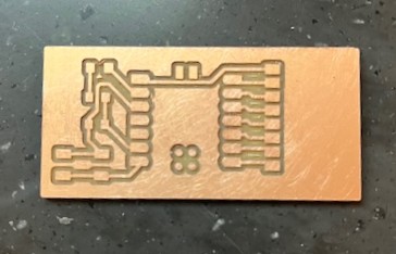
Milled Board
Once the board is fully cut you need to remove it from the machine. I used a metal scraper to get the copper sheet and cut board out of the machine. You have to be careful to not bend the sheet too much so it doesn’t snap. After scraping off the remaining tape, I needed to sand the cut board a bit. I got a square of sandpaper wet and lightly sanded by going in small circles. You have to be careful to not damage any of the traces. With this, I had a fully cut out circuit board!
Soldering
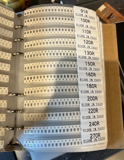
Resistor Book
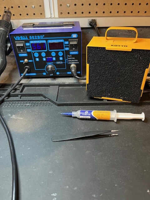
Soldering Station
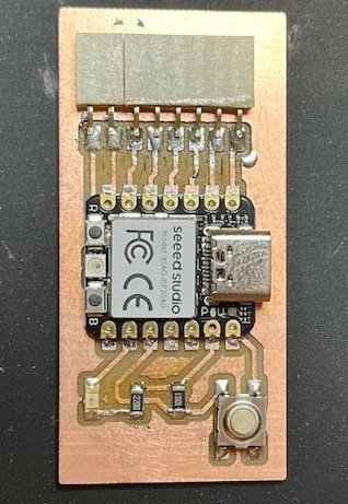
Fully Soldered Board
Next is to solder the components onto the board. I used the PCB design that I made in KiCad as a reference for this step. I started by gathering all of the components that I needed. My lab has a book of resistors that have the resistors on strips sorted by resistance. I didn’t actually take my resistors from here because they had the more common values in bulk elsewhere, I just thought it was a fun way to store resistors. Before starting, make sure you are working on a heat resistant surface and have some sort of ventilation. My lab has a little fan at the soldering station. I used flux paste to solder everything to the board. To use it, you squeeze a little bit of the paste onto whatever pad(s) you want to solder and place your component on top. Then using a heat gun, blow hot air onto the paste until it melts and becomes a liquid shiny silver. I had the heat gun set to about 700 degrees fahrenheit. It’s easy to blow your pieces out of place with the heat gun, so I used tweezers to hold some of the smaller components in place. I continued this process until I had all of the components on the board.
Testing
To test the board I made a program that turns on the LED when the button is pressed. I used this example on Wokwi as a structure for the code. I could have figured it out myself but I kept getting pulldown and pullup resistors mixed up. My circuit has a pulldown resistor on the button. I used the Arduino IDE to transfer the code to the board. As you can see from the video, my board and the code works!
        //TURN ON LED WHEN BUTTON IS PRESSED

        const int buttonPin = D9;
        const int ledPin = D8;
        int oldValue = LOW; // default/idle value for button is low

        void setup()
        {
          // Initialize the pins for reading from button and writing to LED
          pinMode(buttonPin, INPUT);
          pinMode(ledPin, OUTPUT);
        }

        void loop()
        {
          // Read the value of button
          int newValue = digitalRead(buttonPin);

          // Check if the value was changed
          if(newValue != oldValue)
          {
            if(newValue == HIGH)
            {
              digitalWrite(ledPin, HIGH);
            }
            else
            {
              digitalWrite(ledPin, LOW);
            }
            // Remember the value for the next time.
            oldValue = newValue;
          }
          delay(100);
        }