Week 6: Electronics Design
Group Assignment
This week’s group assignment was about using tools to observe the operation of a microcontroller. You can find my group’s documentation here.
This was more of a review for me since I have worked with circuits before, though most of my experience is on breadboards. I was reminded that multimeters are a very useful tool because they can measure both voltage and resistance. You can also measure the voltage of a subsection of a circuit based on where you place the prongs. We demonstrated this by measuring the voltage at different parts of a circuit that just had an LED and a resistor. Oscilloscopes give more details as to what is happening because you can see a graph of the voltage over time. However they seem to take a bit more time to use effectively because you have to find the correct scale.
Learning KiCad
Setting up KiCad
I started by downloading KiCAD 9 and going through the installer. However before getting started, I had to install the Fab Electronics Library for KiCad so that I could use electronics that are commonly kept in Fab Labs. To install the library I followed the steps in the README file on gitlab.
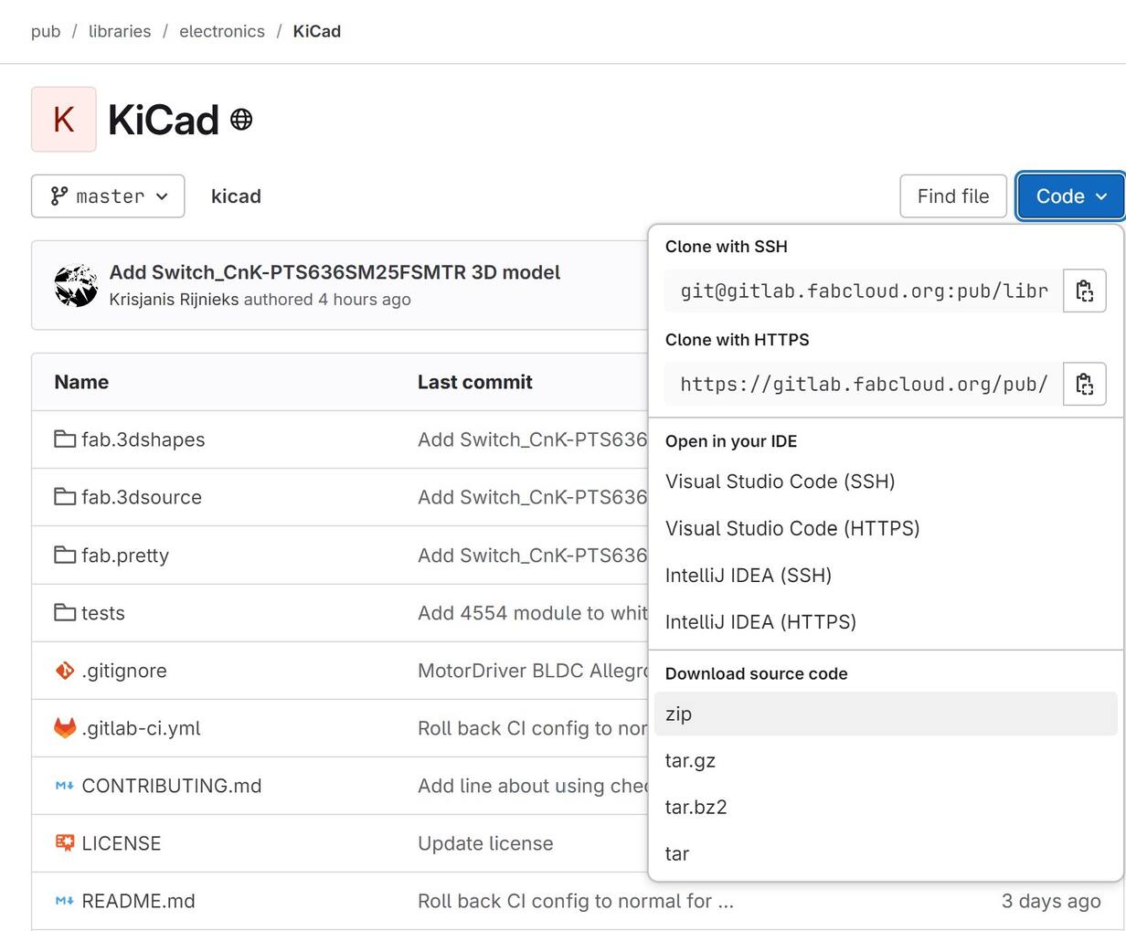
Download Library from Gitlab
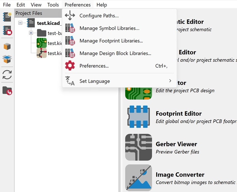
Preferences Menu
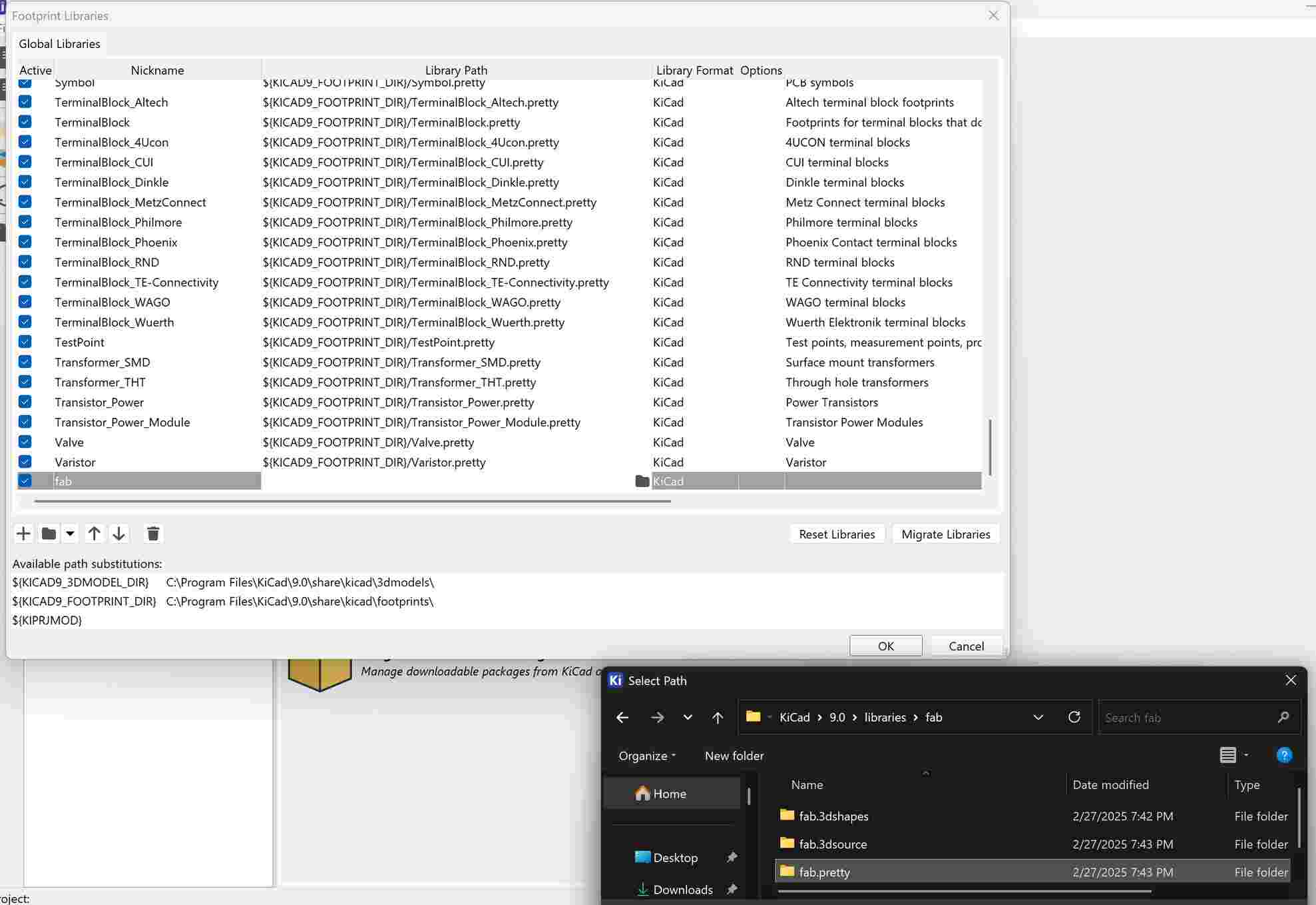
Configuring Paths
To start, go to the blue code button on gitlab then to zip under “Download source code”. Next, I created a folder named “libraries” in the KiCad->9.0 folder. I extracted the zip file, named it “fab”, and placed it in the libraries folder. With that in place, you can then open KiCad. Then go to Preferences -> Configure Paths. Then create a new entry in the shown table by using the plus button in the left corner underneath the table. I just named it fab to match the library. If you are on a windows computer, make sure whatever name you choose is all lowercase. In my local session, the people who are on Windows and used an uppercase character had an error when trying to use the Fab library. Next, select the fab.pretty folder using the folder icon on the right side of the Library Path box. When complete, make sure to press Ok. The next step is to go to Preferences -> Manage Symbol Libraries and add the fab.kicad_sym to the table the same way you added an entry to the paths table. Finally, go to Preferences -> Manage Footprint Libraries and add fab.pretty to the table in the same way as the last two. After this, you should be all set to use the Fab Academy KiCad library!
Basic Circuit
In our local lab session, we went over a simple circuit that just consisted of a XIAO RP2040, a resistor, and an LED. I’m going to go over how to make this to get some of the basic KiCad tools out of the way.
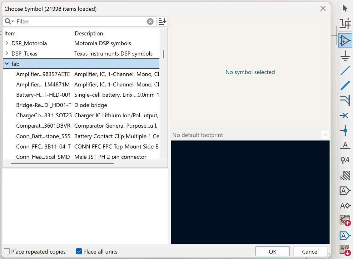
Add Component/Symbol
Edit Details
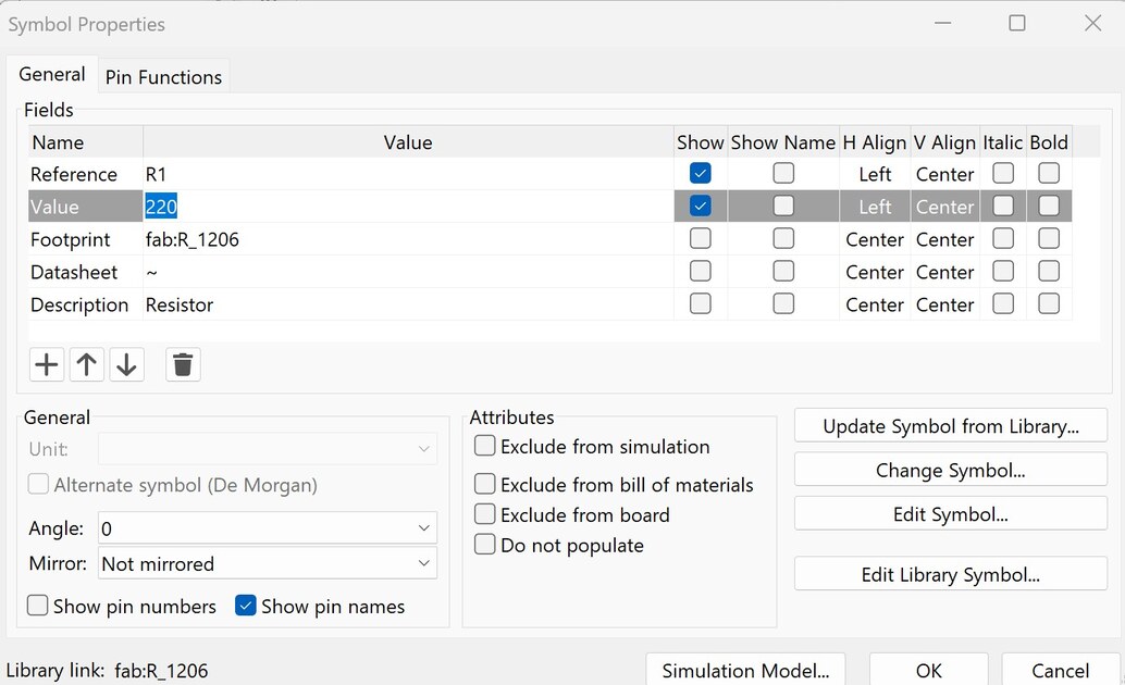
To start a new project, go to File -> New Project. You’ll likely want to start with making a schematic, so select Schematic Editor from the list of tools on the right. First, you should add the components you want to use so that you can wire them together. In the right column, go to the triangle with a plus and minus sign in it, which is highlighted in the above image. You will then see a list of all possible components. You’ll likely want to use the search function to find whatever components you want. If you want a part that is from the Fab Academy library, then you can type in the name of your part with the word fab, and matching items in the fab library show. It was recommended that we use the 1206 version if it’s an option because that is a fairly common size. Once you’ve selected your part, just click somewhere on the screen to place it. When you’re done using any tool, including Place Symbols, you can hit the Select Item(s) button or just press esc. Using the select tool, you can move around any parts you have already placed. If you select a symbol and then double click on it, a menu will appear that will allow you to change certain details of it. For example, we changed the resistor’s value to 220 because if this was an actual circuit we would want a 220 ohm resistor. This isn’t a requirement but it makes the circuit easier to understand and build if you’re using the schematic as a reference.
Add Wire
Add Power Symbols
Example Schematic
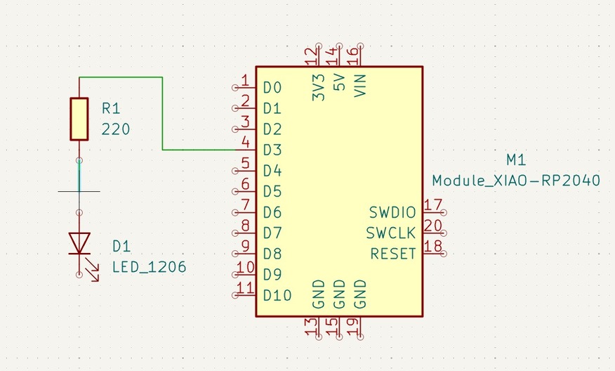
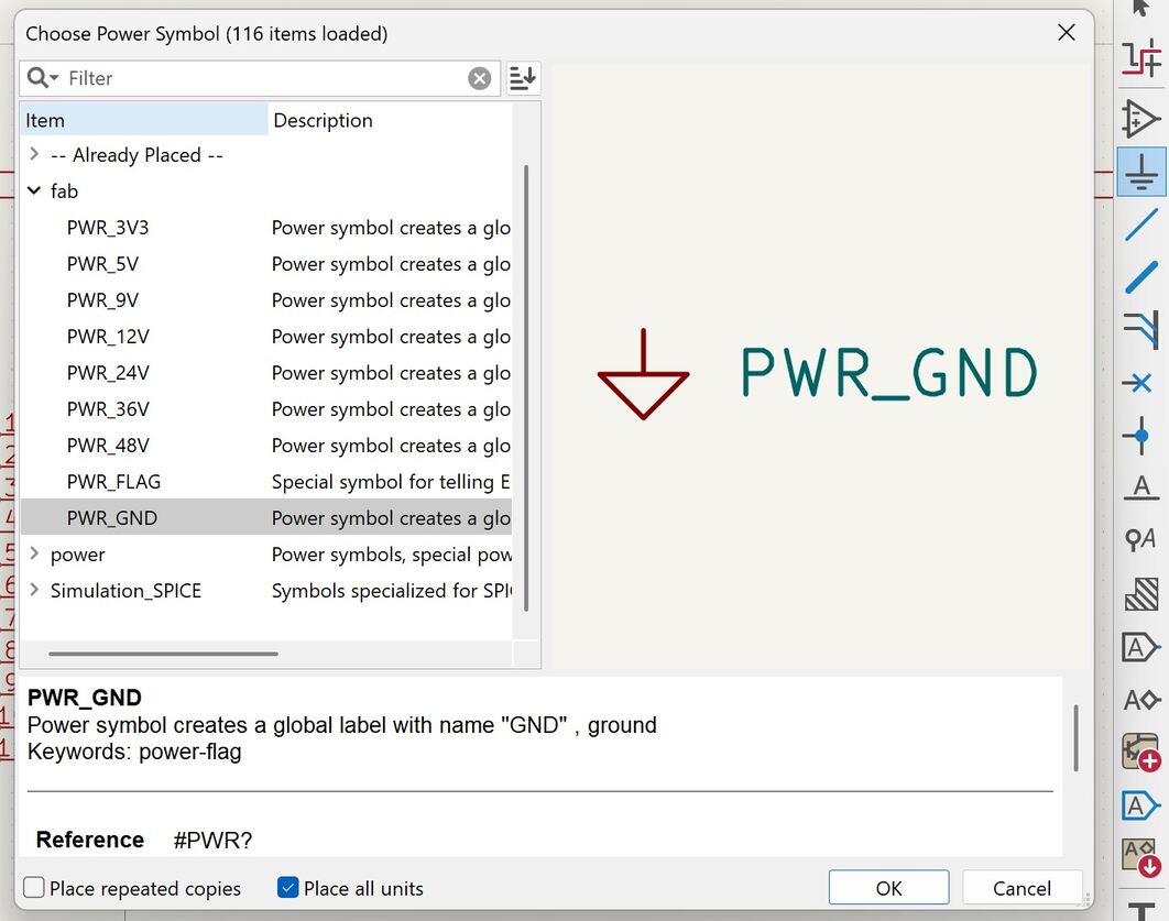
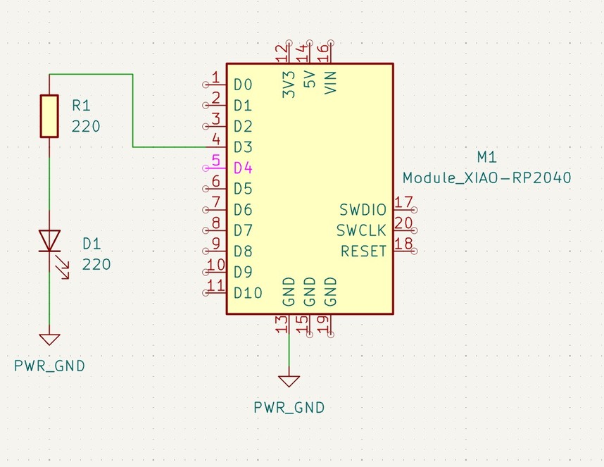
Once you have all of your symbols placed, you can start connecting them. There is a Draw Wires option in the right column. You can also just click on a node when you’re in select mode. Either way, once you’ve clicked on the node, click on the other node you want to connect it to. You can also click on empty space before connecting the wire to the second node if you want it to look more organized. If you can also add Power Symbols by hitting the ground symbol in the right column. They act as a portal from one spot to another and can make your schematic look more organized. In this example, I used the ground power symbol with one end connected to the microcontroller’s ground and the other connected to the ground in the circuit. It isn’t needed for a circuit this small but it’s a handy tool to remember. With this, the example schematic is complete.
Update PCB Editor
Board Setup
Add Routes
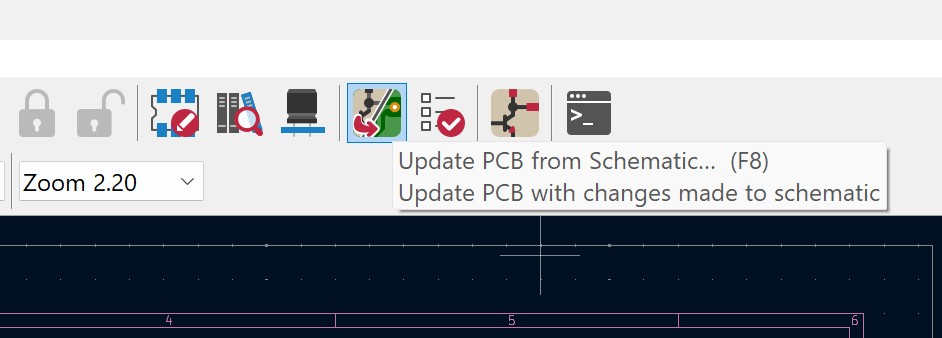
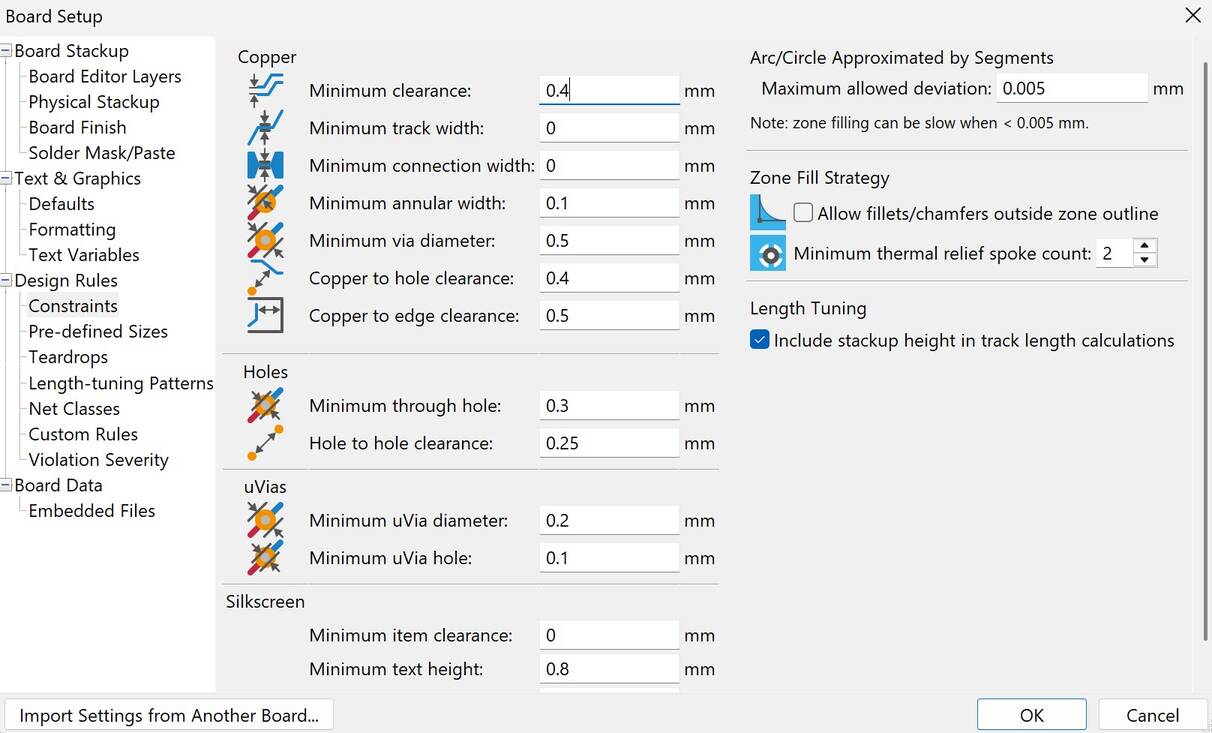
Once the schematic is complete you have to bring it into the PCB editor. To do this, you can go back to the main screen and select the PCB editor. You can also hit the PCB editor button, which is the farthest right in the top bar. Once in the PCB editor, hit the Update PCB From Schematic button, which is the top right and is half green and half tan. This will bring over your schematic. You can change the design rules your board must follow. Go to File -> Board Setup to change the settings. I changed my settings to follow these instructions. The important things to change are the “Minimum Clearance” and “Copper hole to clearance” settings under Design Rules -> Constraints because this is directly affected by what size cutting tool you will be using to mill your circuit. Changing these settings will make it so the routes aren’t too thin to cut. I changed mine to 0.4mm since that is the diameter of the most commonly used cutting tool.
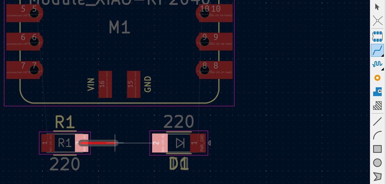
As with the schematic editor, you can use the select tool to move around any components. You can also rotate them by pressing ‘R’ when the component is selected. The next step is to wire together the parts, which is called routing. Go to the Route Single Track tool which is a wire symbol on the right sidebar. When you click on a node, a thin blue line will appear which tells you which node you need to connect it to. As with the wiring in the schematic, you can click on empty space to organize your routes. An important fact is that the routes can’t cross because these are the lines that will be cut into the circuit board. However, routes are allowed to go under other components, like the microcontroller. You can also change the width of the routes. The size route you can cut is limited by the machine you’re using and the bigger it is, the easier it will likely be to mill. You can change this by double clicking on a selected wire and changing the Track Width setting. I changed it to 0.4mm by recommendation of my local instructors.
Outline Board
Design Rule Checker
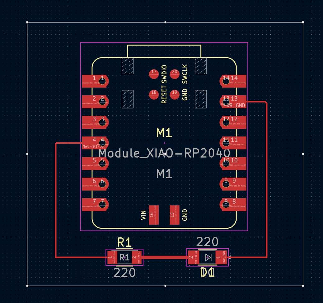
Example PCB Design
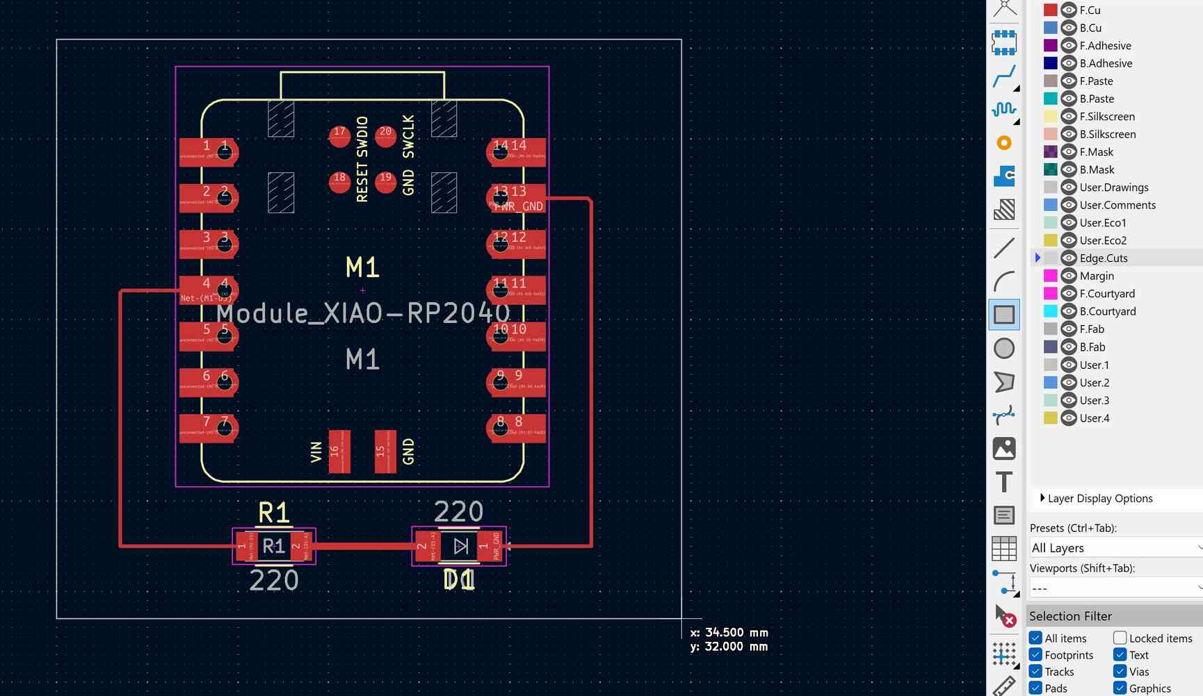
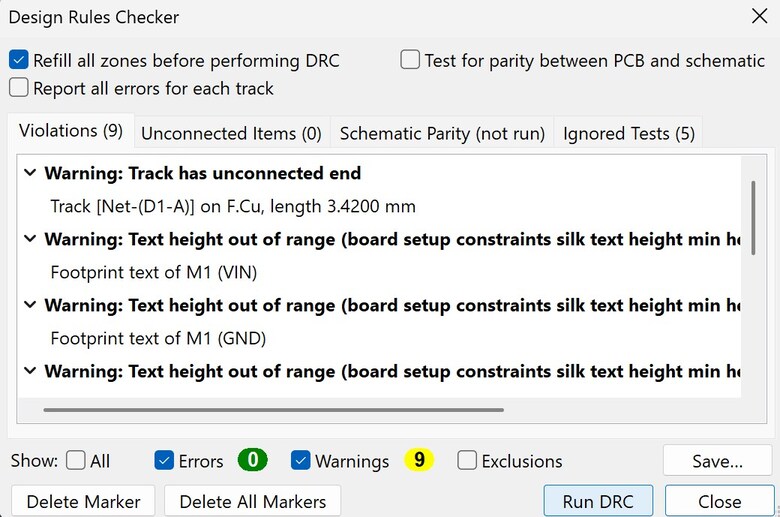
Once everything is routed together, you need to set an outline for the board. You can do this by selecting the Edge Cuts layer and then choosing Line, Arcs, Circles, Rectangles, or Polygons tool. These are all on the right sidebar. For this example, we just did a rectangle. Last but not least, you want to check that your design meets all design rules. To do this, go to Inspect -> Design Rules Checker and hit the Run DRC button in the bottom right corner of the window. It is generally fine if you have warnings but if you have any errors you need to fix it. For example, I forgot to add the board’s outline when I first checked it and was able to figure out what was wrong based on the error message. It will also throw an error if things aren’t connected together correctly. You are then free to export your design!
Designing a Development Board
I decided to design a board that has an LED, button, and 3 prong connector that a servo motor could attach to. I’m thinking about using a servo motor in my final project. The LED and button may be helpful for testing so I included them. I used these parts in the KiCad schematic editor:
- 1206 LED in fab library
- 1206 resistor in fab library
- Microcontroller: XIAO-RP2040 in fab library
- Connector: PinHeader_01x03_P2.54mm_Vertical_THT_D1.4mm in fab library
- Button: Switch_Tactile_Omron in fab library
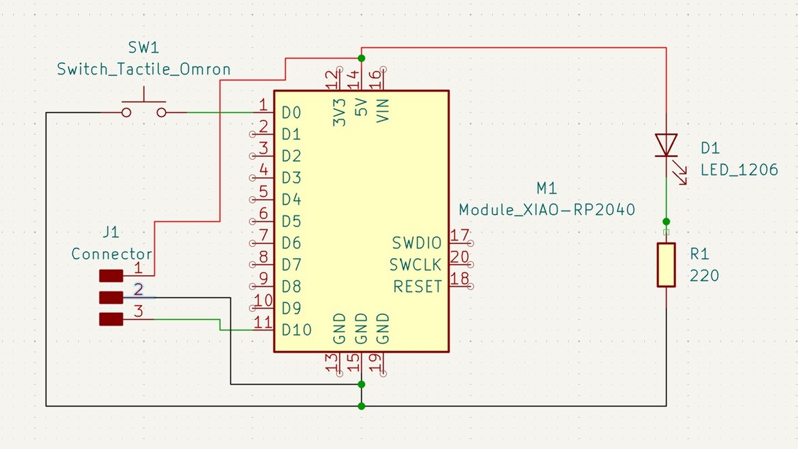
I started by adding all of the parts to the schematic. I did some research and found out that servos commonly have 3 prong female connectors, so I (hopefully) used an adapter that would work with it. The adapter is connected to 5V power, ground, and pin 11 so that the microcontroller can receive input. The button has one side connected to ground and the other is connected to pin 1 so the microcontroller can also receive input from the button. The LED is connected to 5V as well, and then to a 220 ohm resistor. I don’t think this will mess up the other components but they are all connected to the same ground so I’m not sure. When wiring, I made any wires connected to ground black and any connected to 5 volts red. You can change the color of wires by selecting your wire then editing the color option in the Properties window on the left. I also found out that the documentation for some components is linked in the description. If you double click on a symbol to see the Symbol Properties window and look at the Datasheet row there is sometimes a link to the documentation for the component. I found the microcontroller’s documentation helpful to see what pins did what.
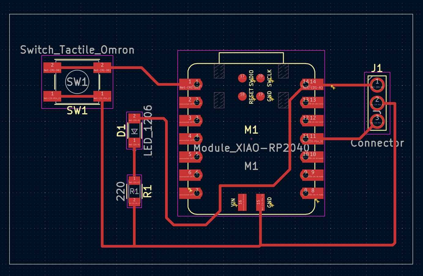
I then had to convert it to a PCB design. After updating the PCB design file, I started routing. Again, it is important for routes to not cross paths unless you want them to be connected. The ground routes run into each other because they all go to ground. I had the 5V line for the LED run under the microcontroller since it was on the opposite side of the board. A note with the button is that it also had me connect the left and right sides of the button together. This is why it’s important to use the Design Rule Checker. Once I had all of the components connected, I used the rectangle tool to draw an outline of the board. After making sure there were no errors in the Design Rule Checker I can call my design complete! I imagine this design is only a portion of what I’ll need to do for my final project. Since this was my first actual try at a board design, I’m okay with how it turned out.