Assignment Brief:
- Characterize the design rules for your in-house PCB production process.
- Submit a PCB design to a board house.
- Design, fabricate, and test a microcontroller development board.
New Week
I am a newbie in electronics design and production. You can refer to my
Week 06
documentation to
understand my attempts and struggles in building a circuit and designing a board. I designed one half of
the electronics for my
Final project
which is mostly a pinout structure of the RP2040. In this week I worked on
working on electronics production—fixing errors, refining the design, and ensuring proper connections.
Debugging, tracing faulty connections, and optimizing the layout are part of my current process.
Also, as it was the first time that I was building a PCB, I stuck to builidng a simple rounded rectangle shaped
PCB only
As the focus for me was the process and functionality.However, for my Final project PCB the plan of action I
have includes
an in organic shape. As the Extend of reach of my Book Nook. Refer to the documentation of my
Final Project to the learn the process
further.
Electronics Production
Electronics production is the process of manufacturing electronic devices by assembling and integrating
electronic components onto a circuit board. It involves designing, fabricating, assembling, and testing
circuits to ensure they function as intended. This process can range from small-scale
prototyping to large-scale industrial manufacturing.
What is a PCB?
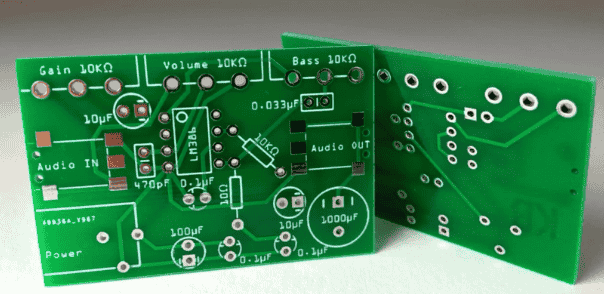
A Printed Circuit Board (PCB) is a flat board made of insulating material (like
fiberglass) with conductive copper tracks that connect different electronic components. Instead of using
traditional wiring, a PCB provides a structured layout for electrical connections, making circuits more
compact, reliable, and easier to manufacture.
Key Parts of a PCB:
- Substrate (Base Material): Usually made of FR4 (fiberglass-reinforced epoxy resin) for
strength and durability.
- Copper Layer: Thin layers of copper act as electrical pathways connecting components.
- Solder Mask: A protective layer that prevents short circuits and oxidation of copper traces.
- Silkscreen: Printed labels on the PCB surface that indicate component placement and reference
designators.
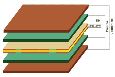
Types of PCBs:
- Single-layer PCB: Has a single copper layer, used in simple circuits.
- Double-layer PCB: Copper traces on both sides, allowing more complex designs.
- Multilayer PCB: Multiple stacked layers, used in advanced applications like computers and
communication devices.
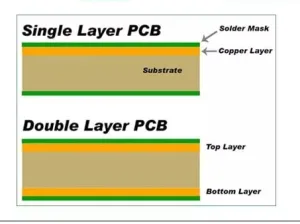
PCB Design and Manufacturing Process:
- Schematic Design: Creating a circuit diagram using software like KiCad, Eagle, or Altium. Refer to
my
Week 06
documentation
- PCB Layout: Converting the schematic into a physical board design with component placements and
copper traces.
You can refer to my
documentation
- Fabrication: The PCB is manufactured using processes like etching, drilling, and applying solder
masks.
- Assembly: Components are soldered onto the board using surface-mount (SMT) or through-hole (THT)
techniques.
- Testing & Debugging: Checking for connectivity issues, short circuits, or faulty components.
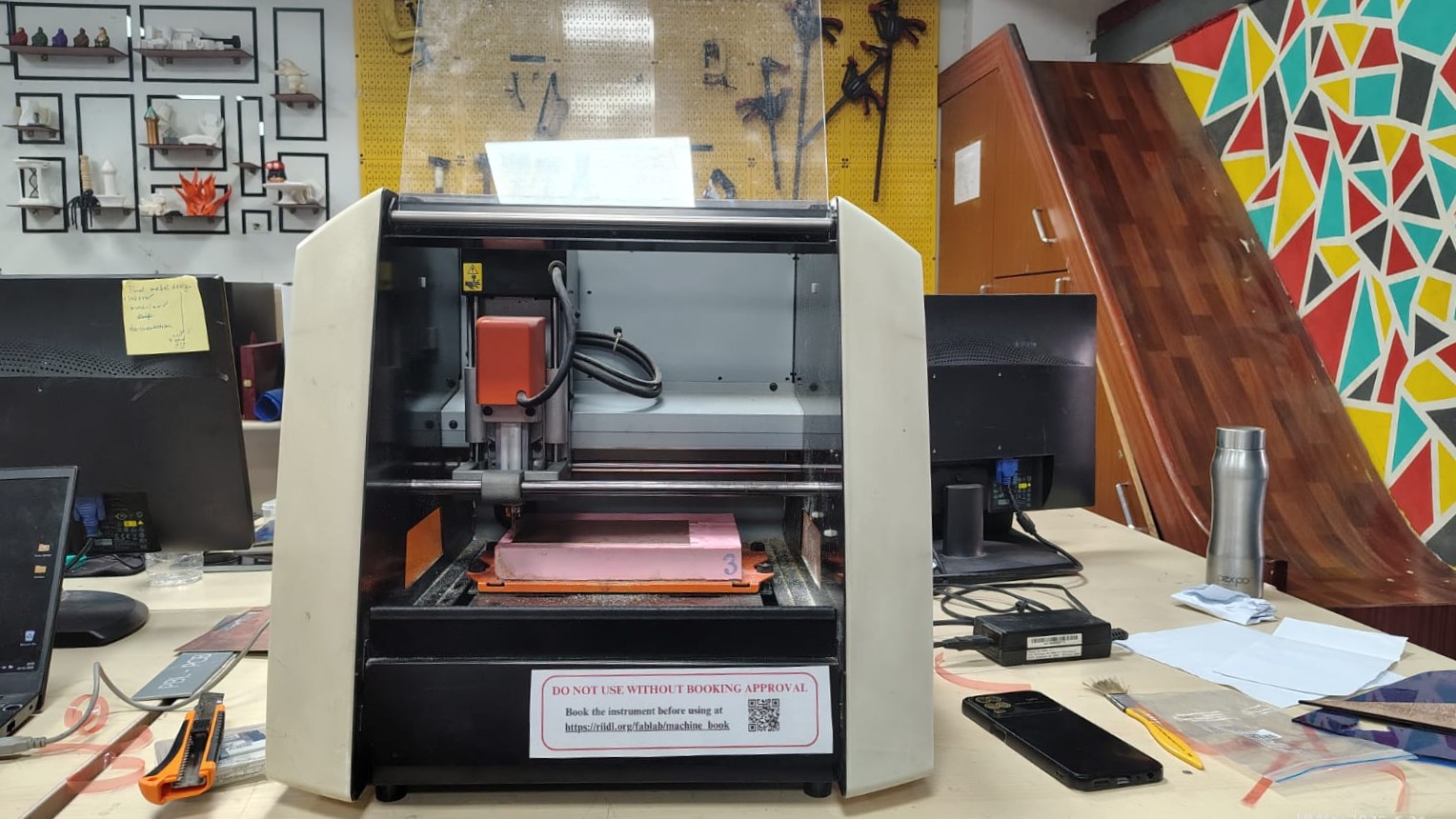
Riidl Fablab: Roland SRM 20
Our Riidl FabLab has two machines for electronic production that are, Roland SRM 20 and Protomat E44. We used
Roland SRM 20
for the production of our PCB. To know more about Roland SRM 20
Click here..
The Roland SRM-20 is a compact desktop CNC milling machine designed for precision prototyping, PCB milling,
and small-scale machining. It’s designed for precision prototyping and PCB fabrication.
The SRM-20 is widely used in engineering labs, maker spaces, and educational institutions for rapid
prototyping and custom circuit board manufacturing.
Features of Roland SRM-20
Compact & Desktop-Friendly – Small size, ideal for labs and workshops.
High Precision Milling – Provides detailed and accurate cuts for PCB fabrication and prototyping.
Enclosed Work Area– Ensures safety by containing dust and debris.
Supports Multiple Materials – Works with wood, acrylic, wax, modeling foam, and soft metals.
User-Friendly Software – Compatible with Roland’s VPanel for easy operation.
G-Code Support – Allows custom toolpath programming for advanced users.
Adjustable Spindle Speed – Enables control over cutting depth and material suitability.
USB Connectivity – Simple plug-and-play setup for easy operation.
.jpg)
The ProtoMat E44 is an entry-level PCB milling machine used for rapid prototyping of printed circuit boards
(PCBs) without chemical etching. It precisely engraves copper layers, drills vias, and cuts board outlines
with high accuracy. The machine supports single- and double-sided PCBs and is ideal for small-scale
production, research labs, and educational purposes. It features automatic tool change, depth control, and a
user-friendly interface. The ProtoMat E44 is commonly used for quick PCB fabrication, RF applications, and
sensor prototyping. We used the SRM20 for the production of our PCB. Lets Deep dive in the process further.
.jpg)
Software: V-Panel for setting the origin.
Before beginning the process my professor,
Akhilesh Zambre guided me to know that the our SRM 20 machine requires two softwares, 1) V-panel for setting
the origin
and 2) CopperCam for milling process. Thus, adding the process to install both the softwares.
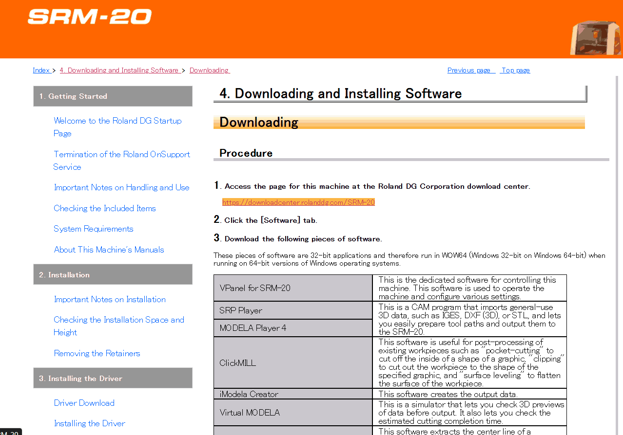
For downloading V-panel
refer to link:
V-panel for SRM 20. The site also has a detailed description of the software and a step by step process of
how to use the software.
As the description of the image below, Click on the link that is highlighted in the image.
Once you click on the link, this page appears> Now click on Software.
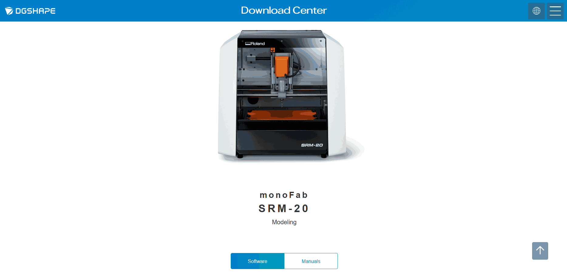
As you scroll down on the page, click on V-panel for SRM-20 and install.
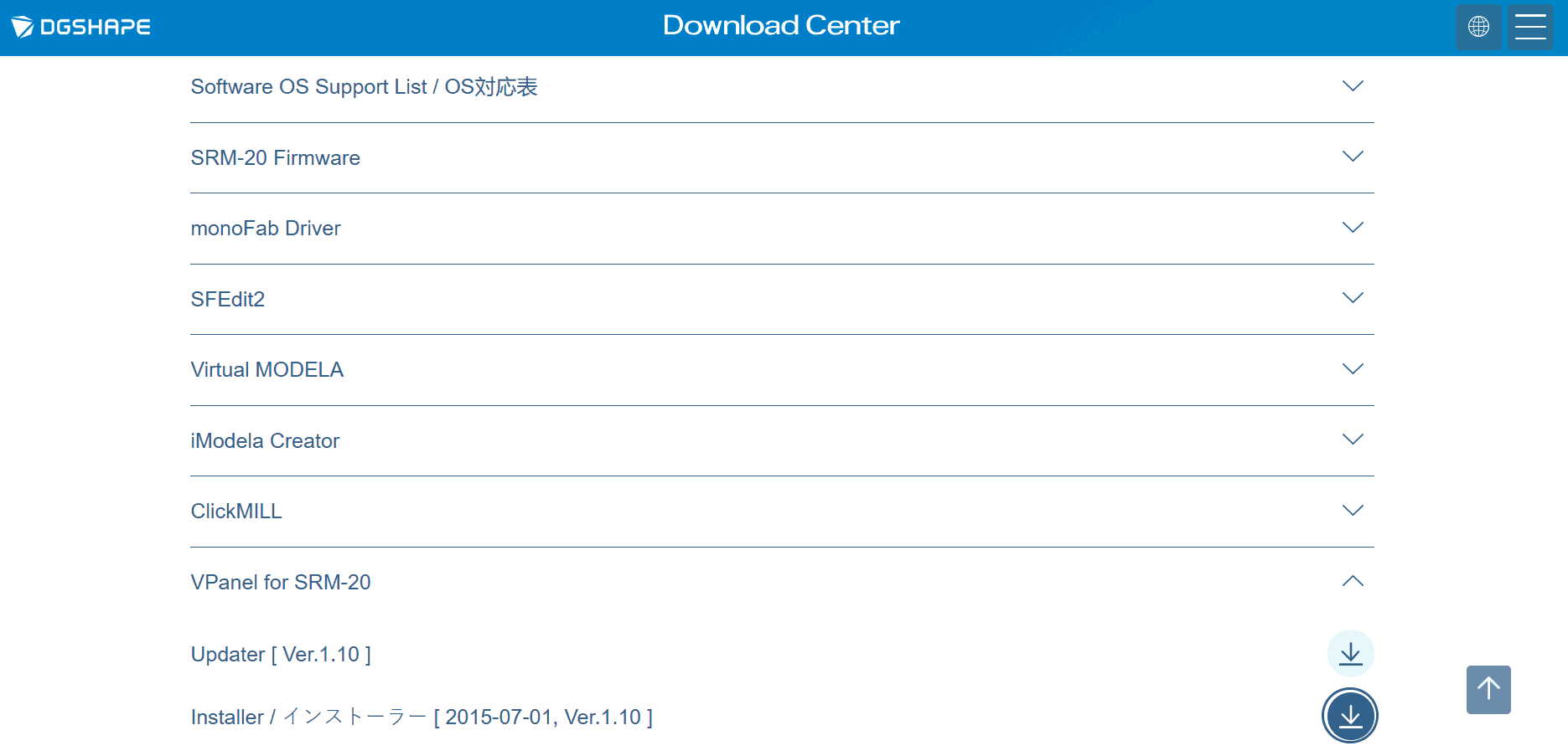
The SRM-20 requires 2 software: V-panel for setting the X-Y-Z axis and origin before setting up the
PCB board design.The Roland SRM-20 CNC machine requires VPanel to set the X, Y, and Z axis origins before milling.
VPanel controls machine movement, spindle speed, and job execution. PCB design software like FlatCAM or Eagle is
used to create toolpaths and generate G-code. You can refer to the PCB that I design
for production in the documentation:
Week o6 of
Electronics
design.
After setting the origin in VPanel, the PCB design is loaded, and
milling is initiated for precise fabrication. Lets understand every process in depth.
V-panel software for setting the origin of the tool bit.
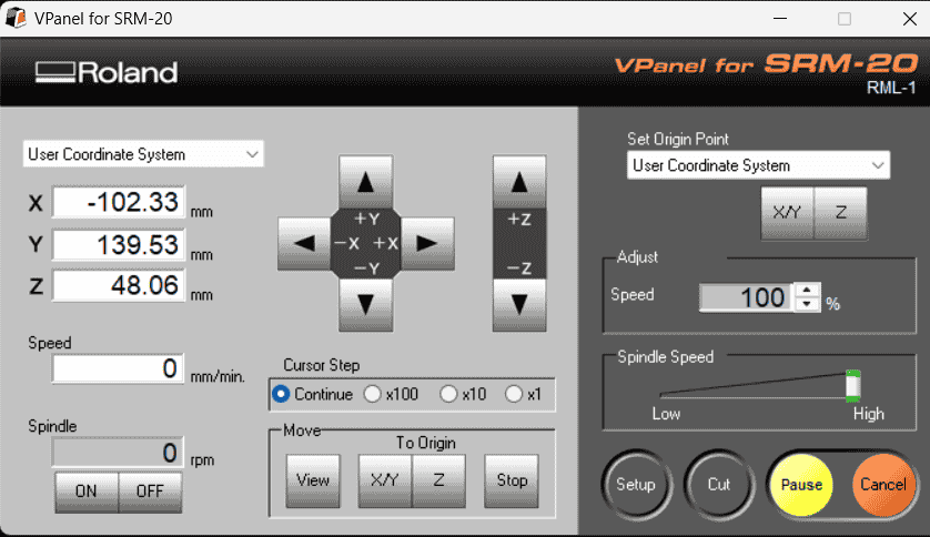
Setting up the machine alongside the software.
Stick a double-sided tape at the base of the copper plate.
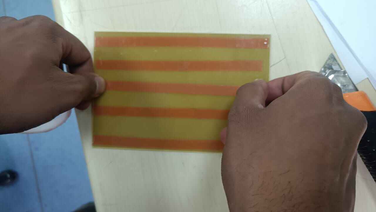
Stick the plate on the pink surface that is the Machinable wax.
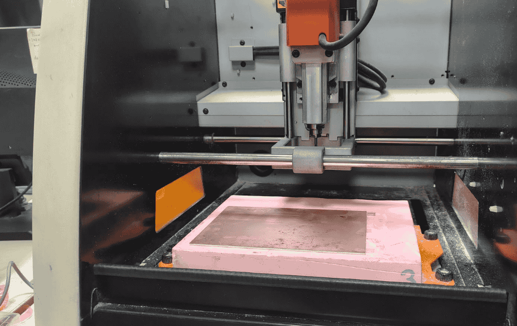
Make sure the
copper plate is stuck firmly to form a plain surface.
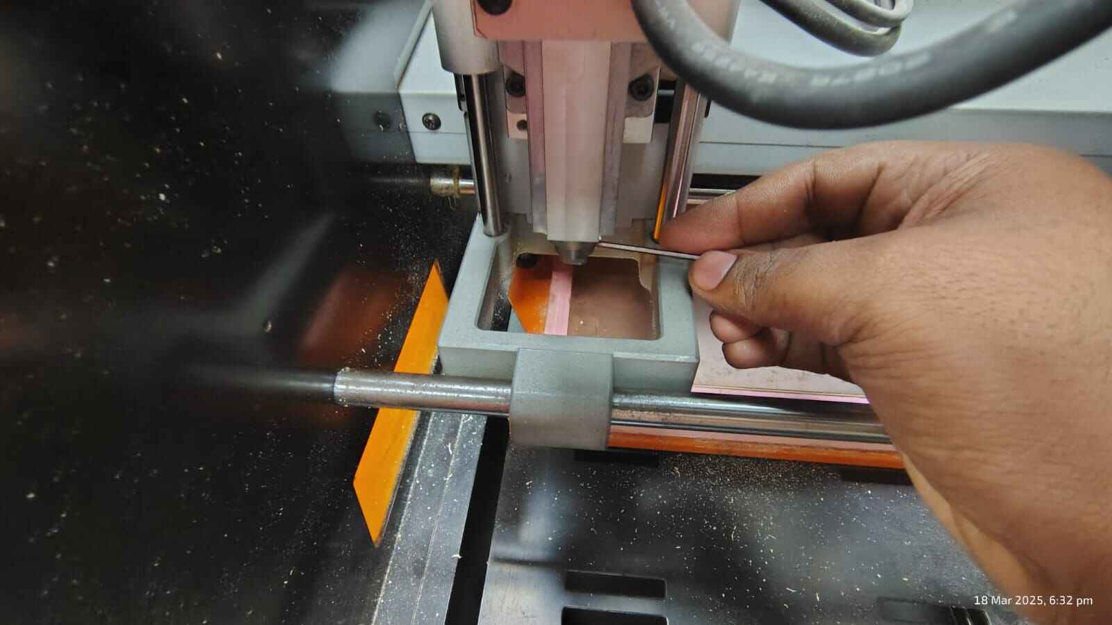
Tool Zeroing process> Setting the tool bit >Use allen keys
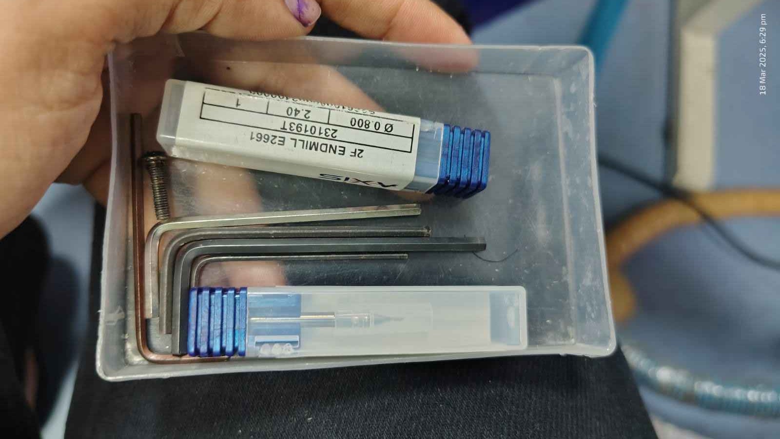
First, we use the 0.2 mm conical bit for engraving tighten using the allen key.
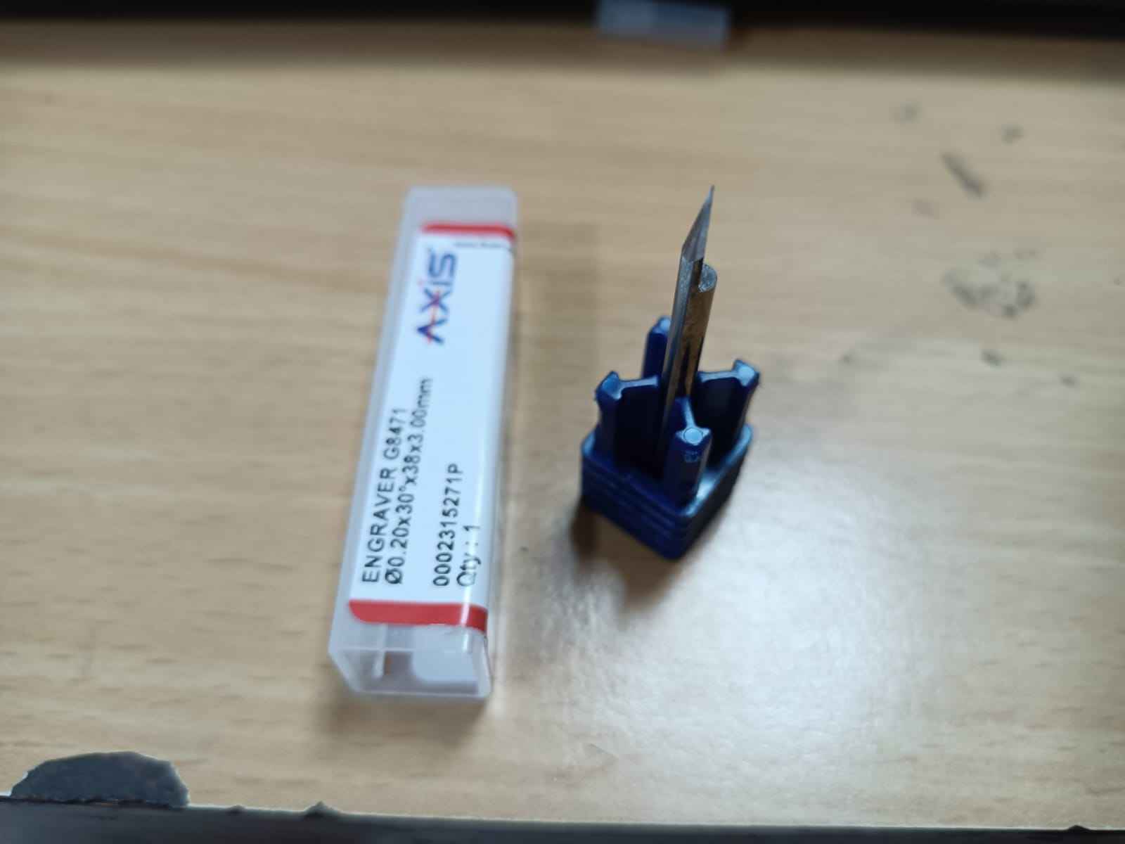
The Tools we used were: 1) Engraver GB471 for engraving layer. Size: Ø0.20×30°×3×3.00mm
which is used for fine engraving work and comes in a protective case,
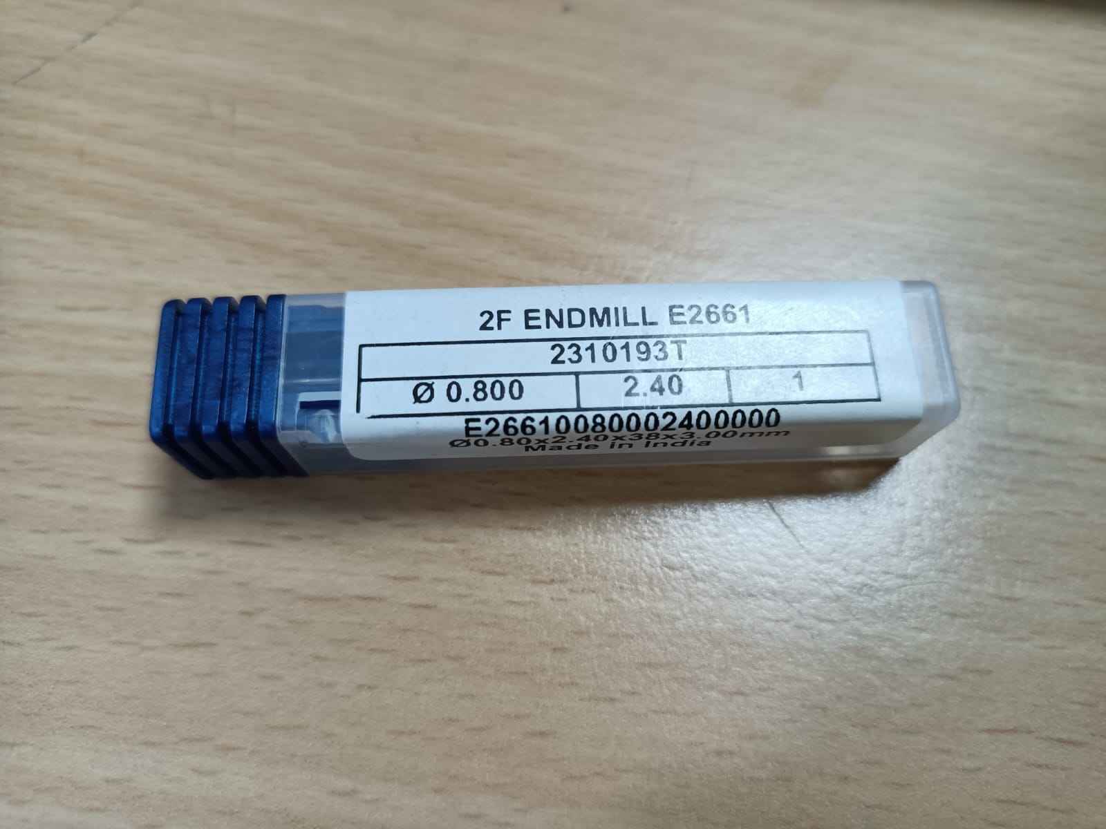
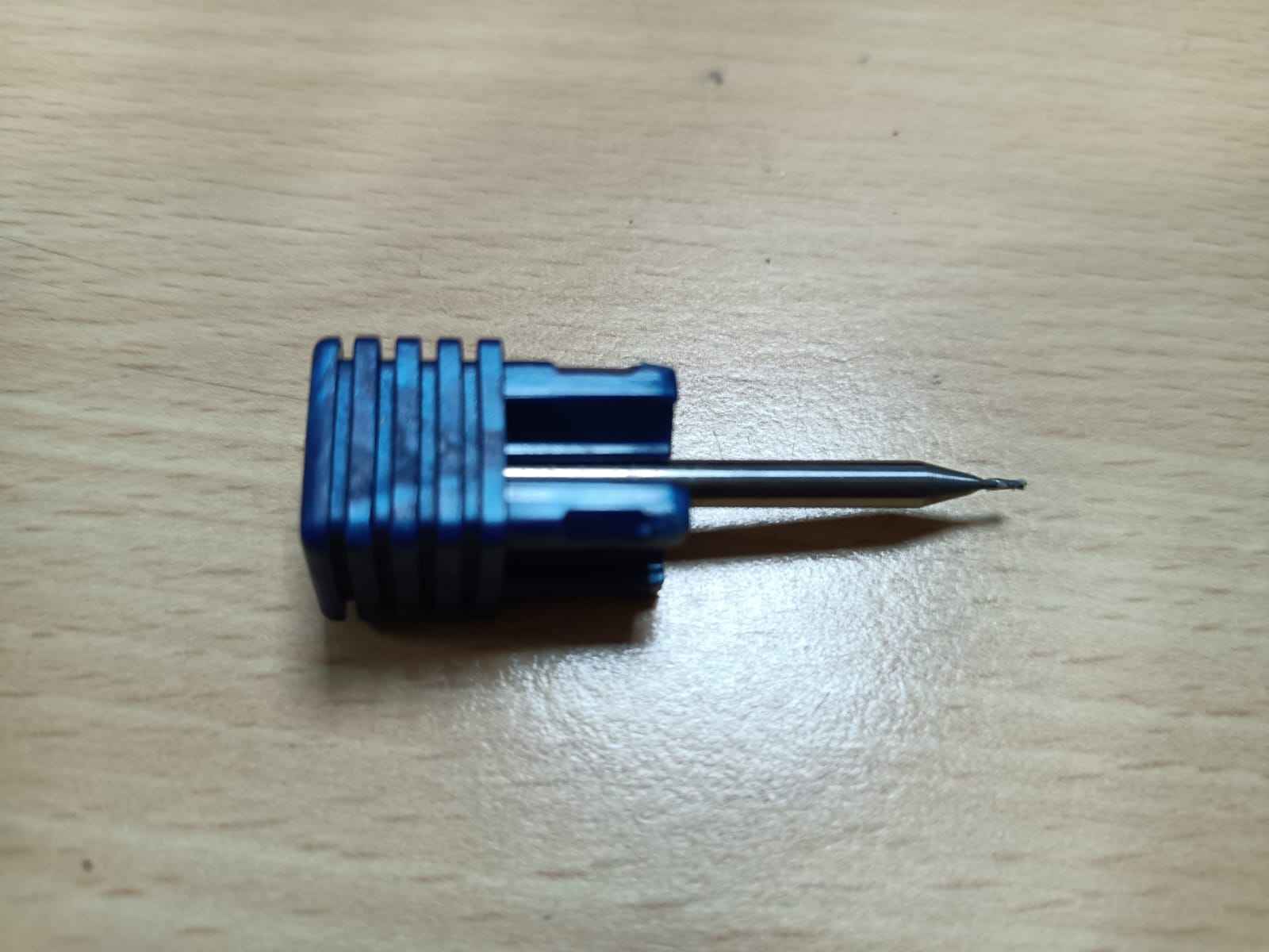
and the tool has a pointed tip for precision. 2)2F Endmill E2661 for cutting and drilling layer. Size: Ø0.800 mm
cutting diameter
Used for cutting or milling operations with two flutes.
The tool is securely packed, and it's advised to close the lid for safety and hit "OK" on the machine before
starting.
Engraver GB471
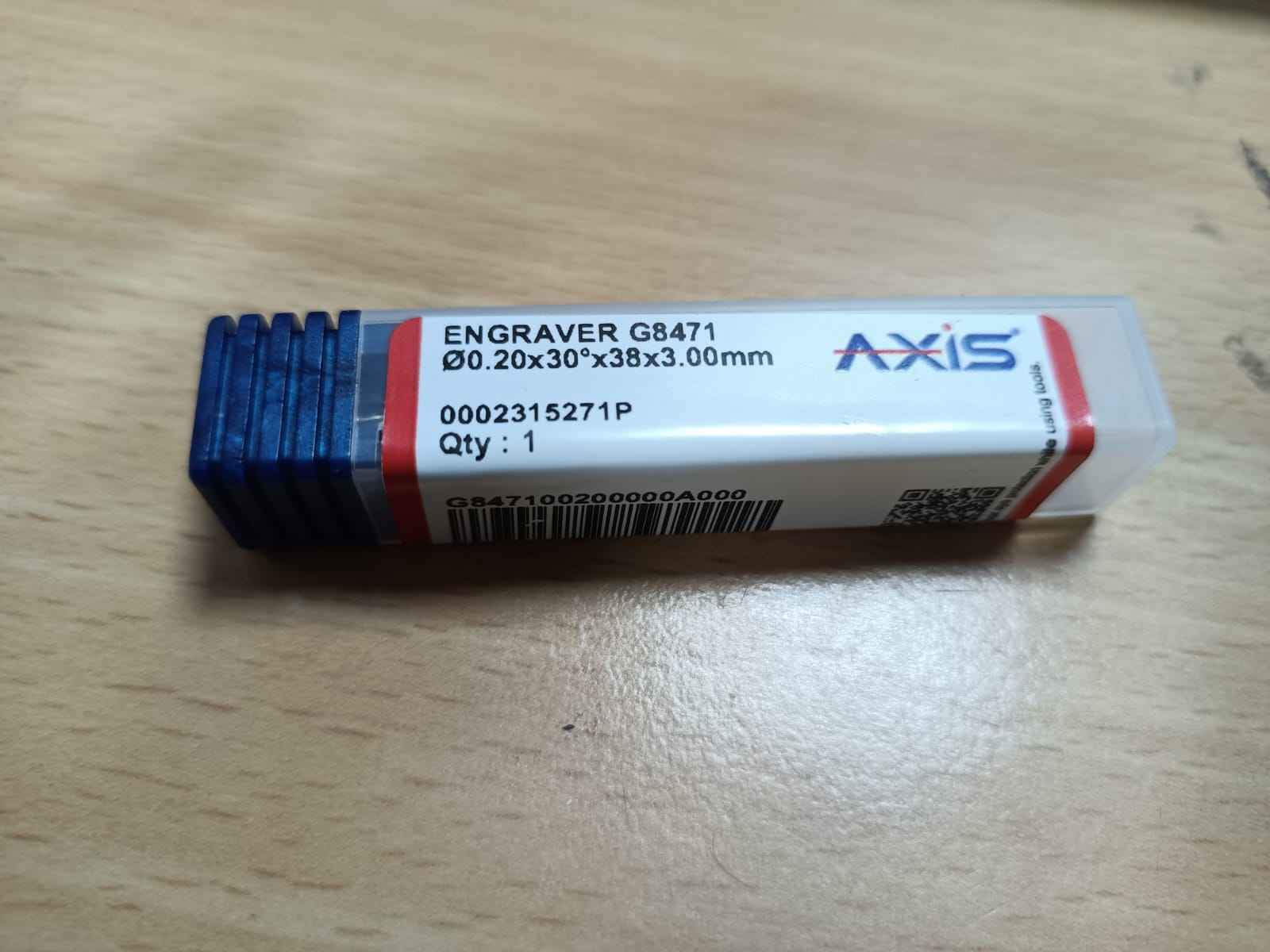
Size: Ø0.20×30°×3×3.00mm
2F Endmill E2661
Size: Ø0.800 mm cutting diameter
Now with the V-panel software, move and bring the tool bit to the closest of the surface of the
copper plate. There are two ways of setting the origin or zero Z-axis here. One is change the
cursor step on V-panel as *1 and the tool just touches the material set the zero axis.
However, the precision in setting the bit in this manner is a bit risky as theses bits unlike the
CNC Bits are a little fragile, and have a possibility of breaking.
We thus, went about with another method, where using the allen key we loosen the
bit slightly from the collet> hold the sides of the bit with soft hands> Smoothly
drop down the bit to the surface base> Make sure the bit doesn't drop down with force.
Set the Zero axis on V-Panel software and SET ORIGIN. Now you can move the bit to any
position but make sure the Z-axis is untouched.
Hold the sides of the bit with soft hands
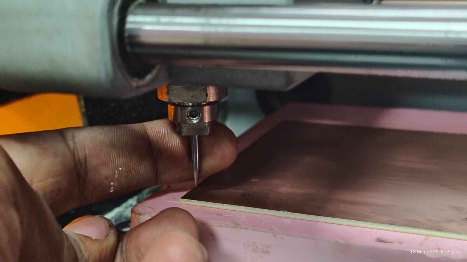
Smoothly
drop down the bit to the surface base
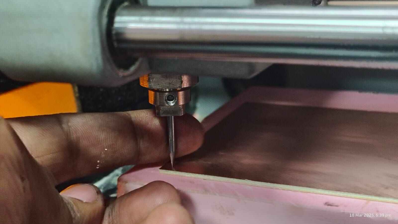
Origin is Set
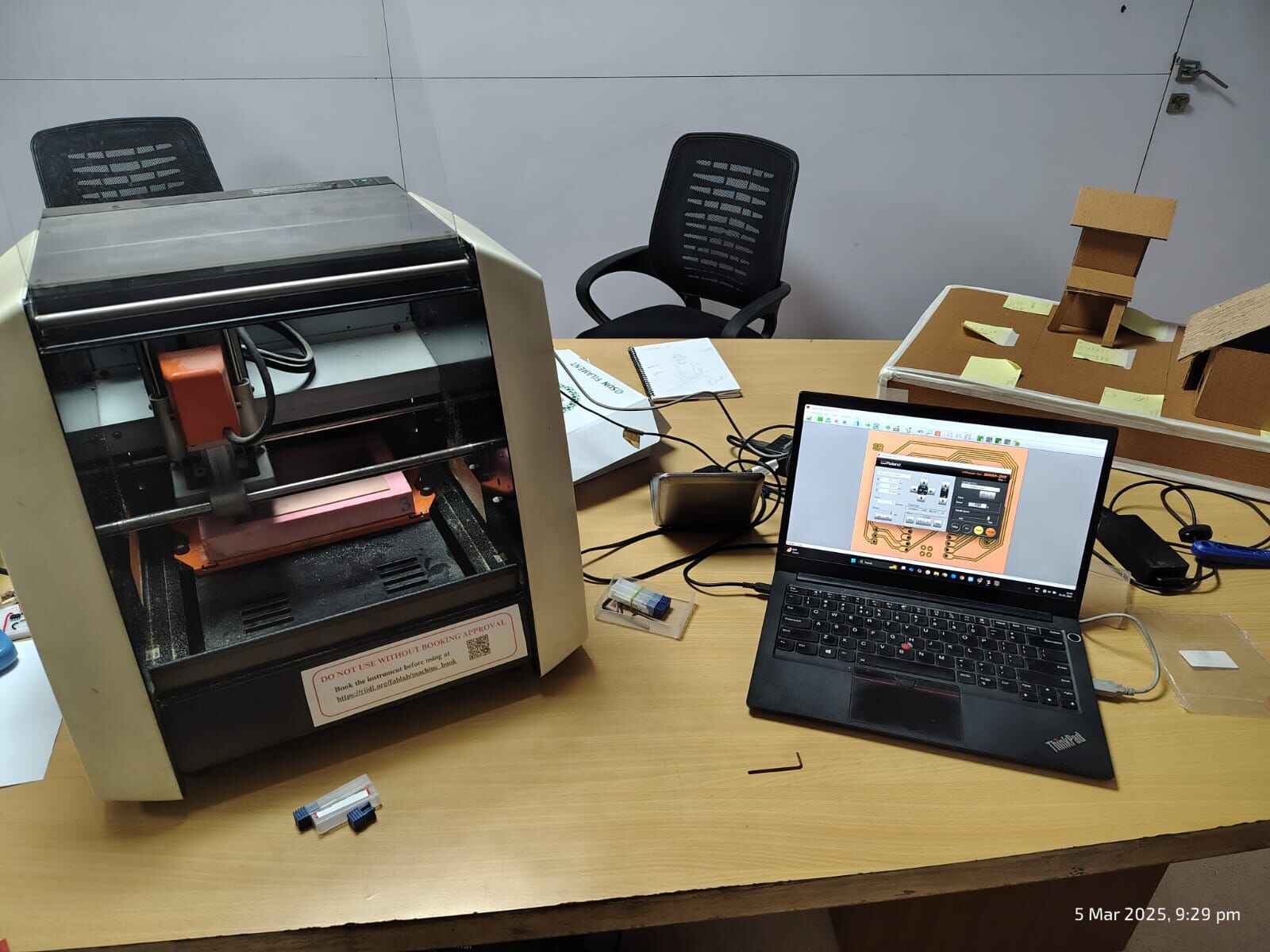
At one point, the milling tool slipped during operation. This incident was particularly insightful, as it
highlighted the fragility and sensitivity of the tool setup. Even minor mistakes in securing the bit can lead to
inaccuracies or damage, emphasizing the need for attention during installation.
Software 2: CopperCam
For downloading CopperCam refer to link:
Copper Cam, this site directly
gives you the page to download
CopperCam> Download and install.
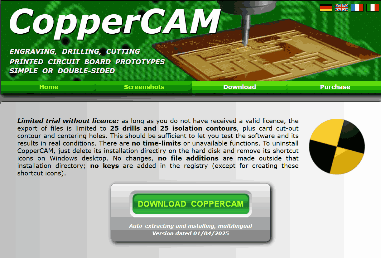
After setting the bit position in VPanel, the Gerber files of the PCB design are imported into CopperCam. In
CopperCam, cutting parameters are set, including tool selection, depth, and milling strategy. Once configured, the
G-code is generated and sent to VPanel to execute the milling process for PCB fabrication.
Lets understand the setting up of CopperCam now.
Parameter> Tools Library
.png)
Change tool settings> here we change to 2, this depends on the machine we use.
.png)
The two Drill bits that we use are:
0.2 mm conical for engraving
0.8 mm flat end mill for drilling and cutting out counters
CopperCam interface
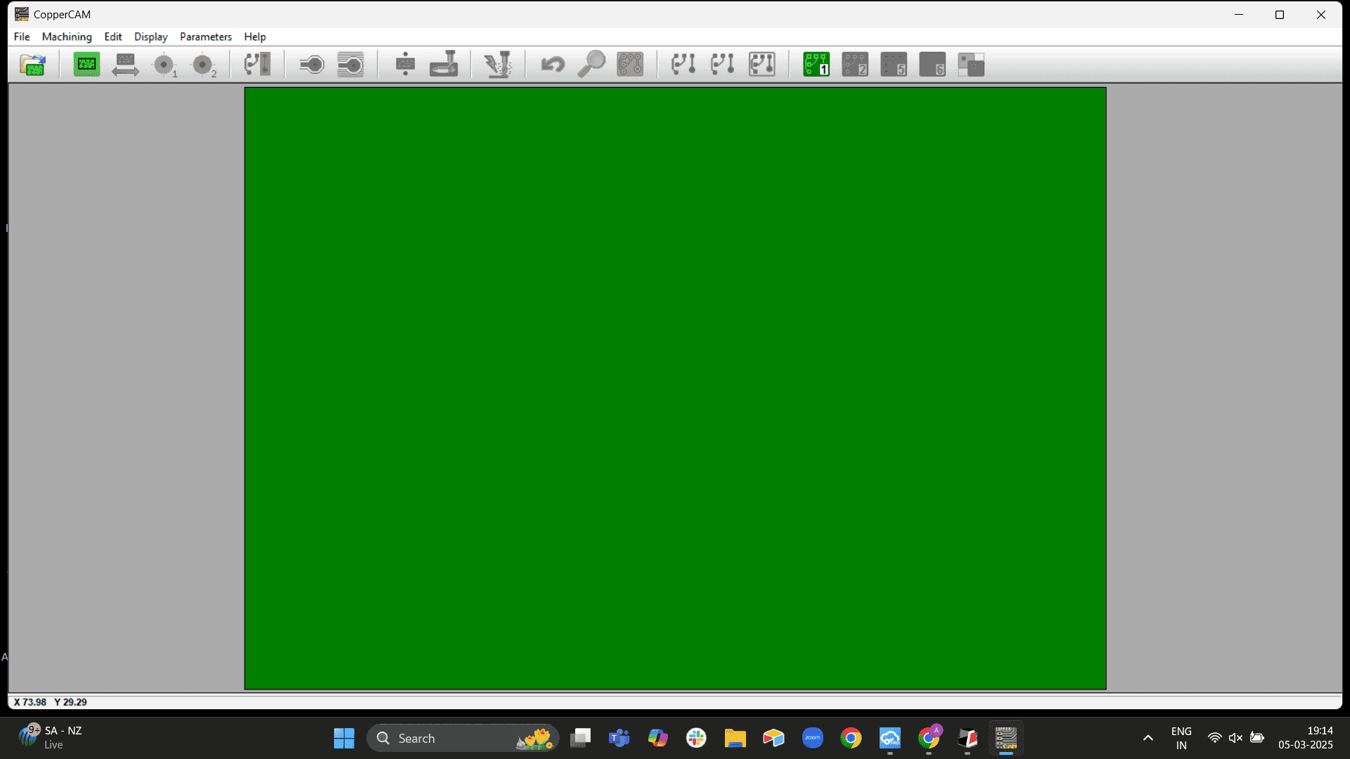
Import Gerber files>
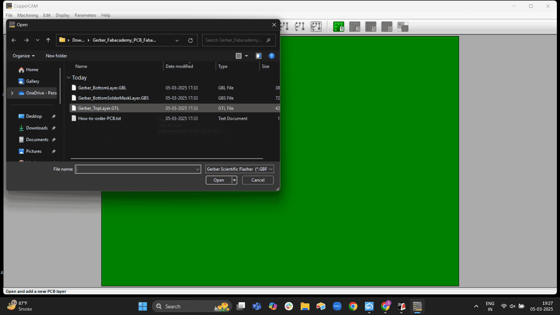
We choose the top engraving layer first as, the
process of engraving requires only a single bit and in the drilling and milling (cutting the outer body) requires
the
flat end bit. We therefore imported the engraving files before.
While importing, left most icon to import engraving layer and right icon for
importing drilling file.
.png)
Selecting the top engraving layer from the local file loacation.

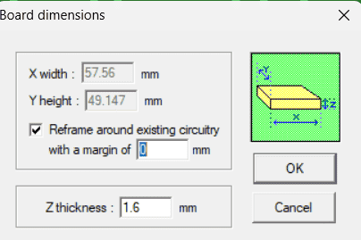
Pop-up, Board dimesions>
1.6 is the material thickness for the machine to analyse cut area.
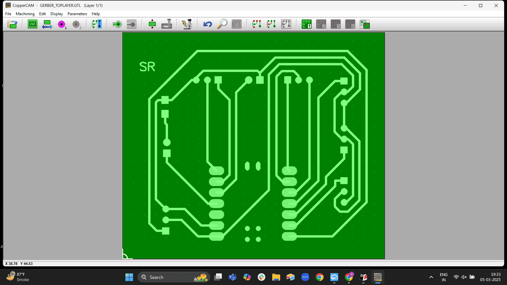
Imported Engraving gerber files>
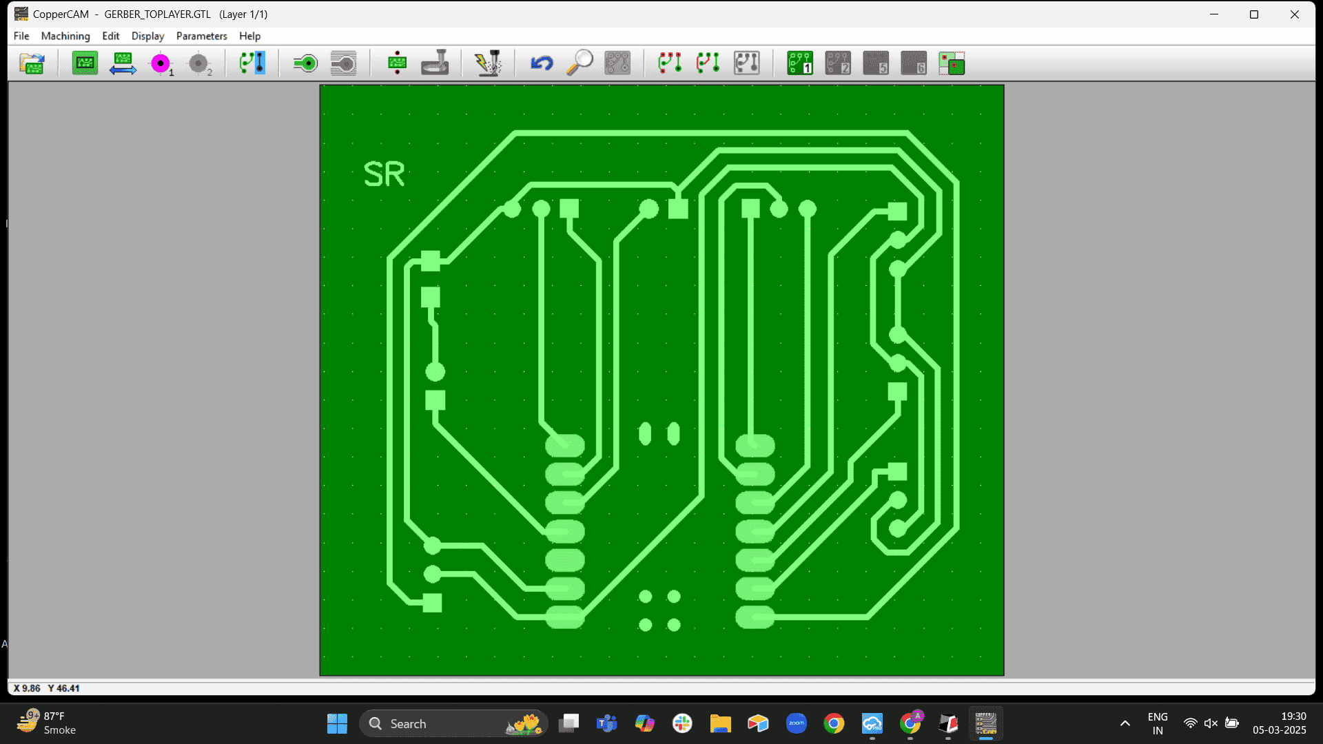
Learnings: As I imported the gerber file, the outer layer which was a curved rectangle,
didnot appear as a cutting area. So with the edit panel, I gave it an exterior recatngle.
Later, after discussing with my professor, I learnt that in my design file, I should have add the external shape
to the
TOP LAYER, which would have cut the outline.
During PCB production, I couldn’t find the outline layer in my Gerber files while importing. To resolve this, I
imported the outline data into PCB Layer 2. Then, I converted this layer into the board outline by selecting
"Convert to Board Outline" or "Convert to Card Contour". This action transformed Layer 2 into the board’s edge
definition, allowing the software to correctly recognize the board shape for fabrication.
In short, Import outline layer to pcb layer 2 then convert the outline to card counter then it will transform that
particular layer 2 to card outline
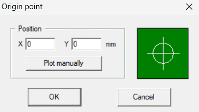
Set the origin of the cut area> File> Orgin
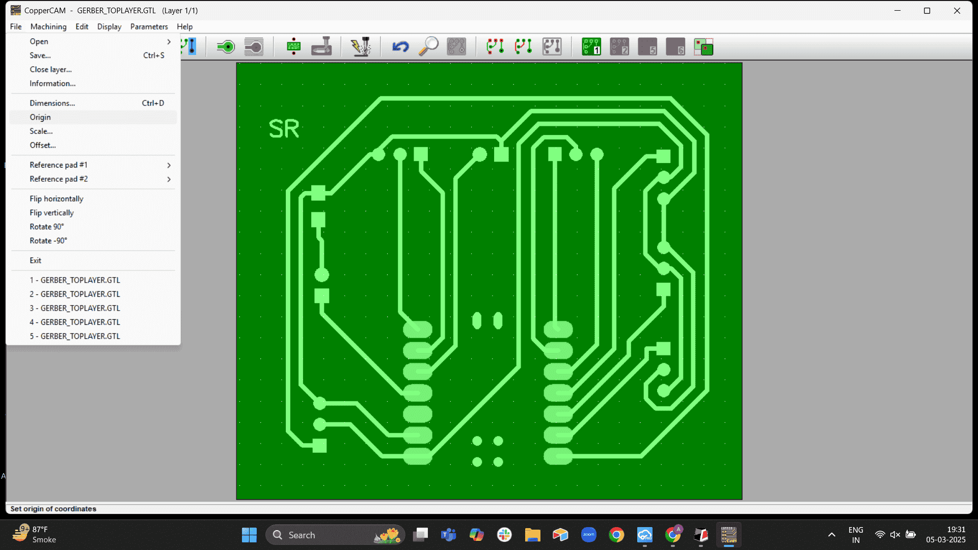
Settings for setting the origin> you can also set the origin manually
at the point of reference as per you design needs.
Once the engraving file is imported, we import the drill file.
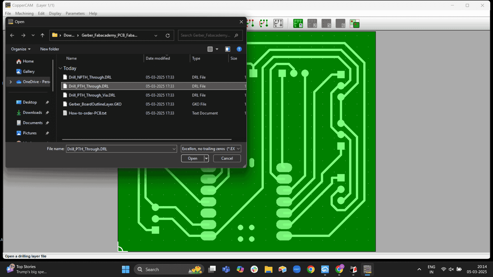
Import Gerber file
Once you import the drill file, Drill holes are
out of place. Match drill holes with the associated
position.
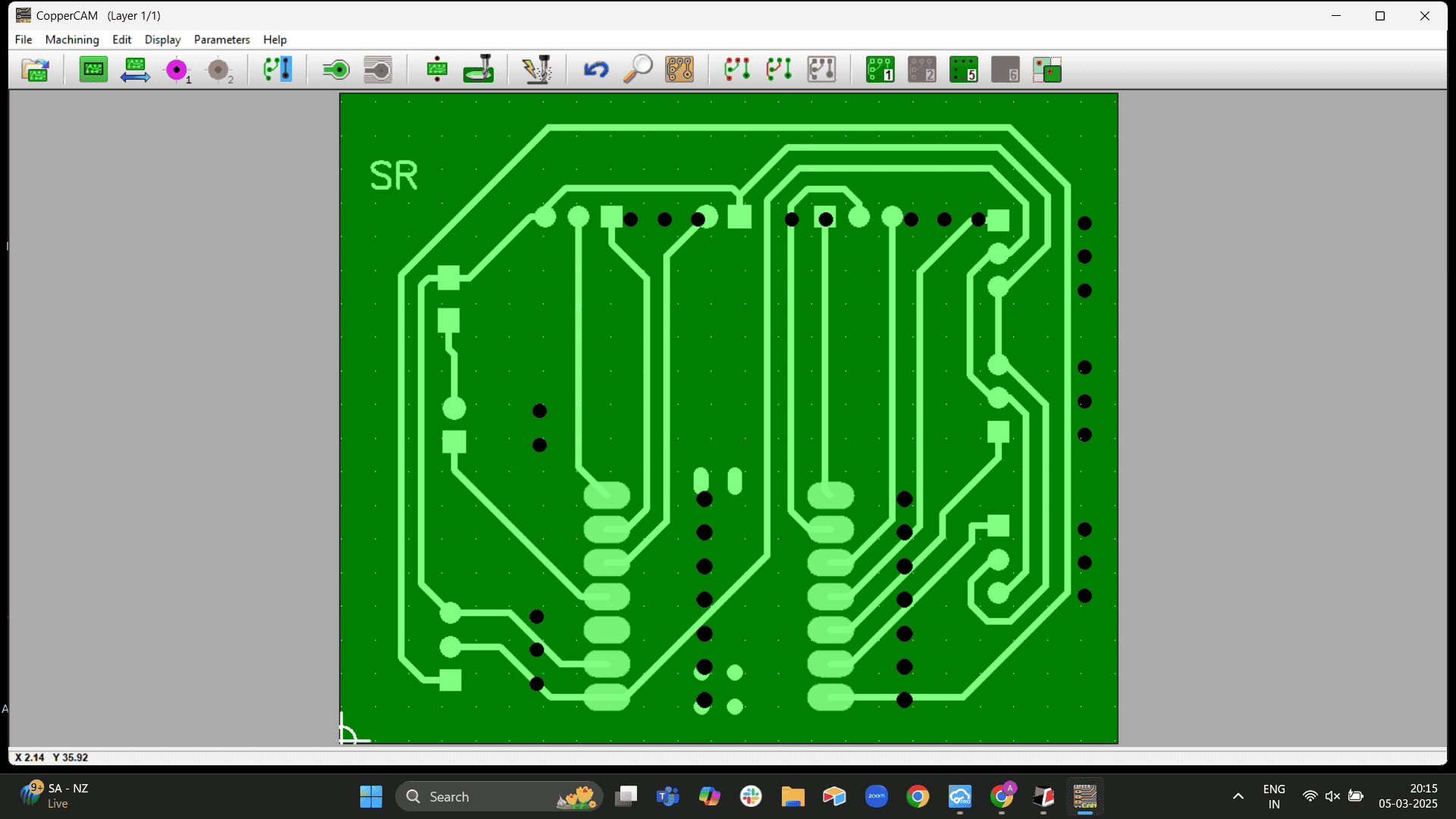
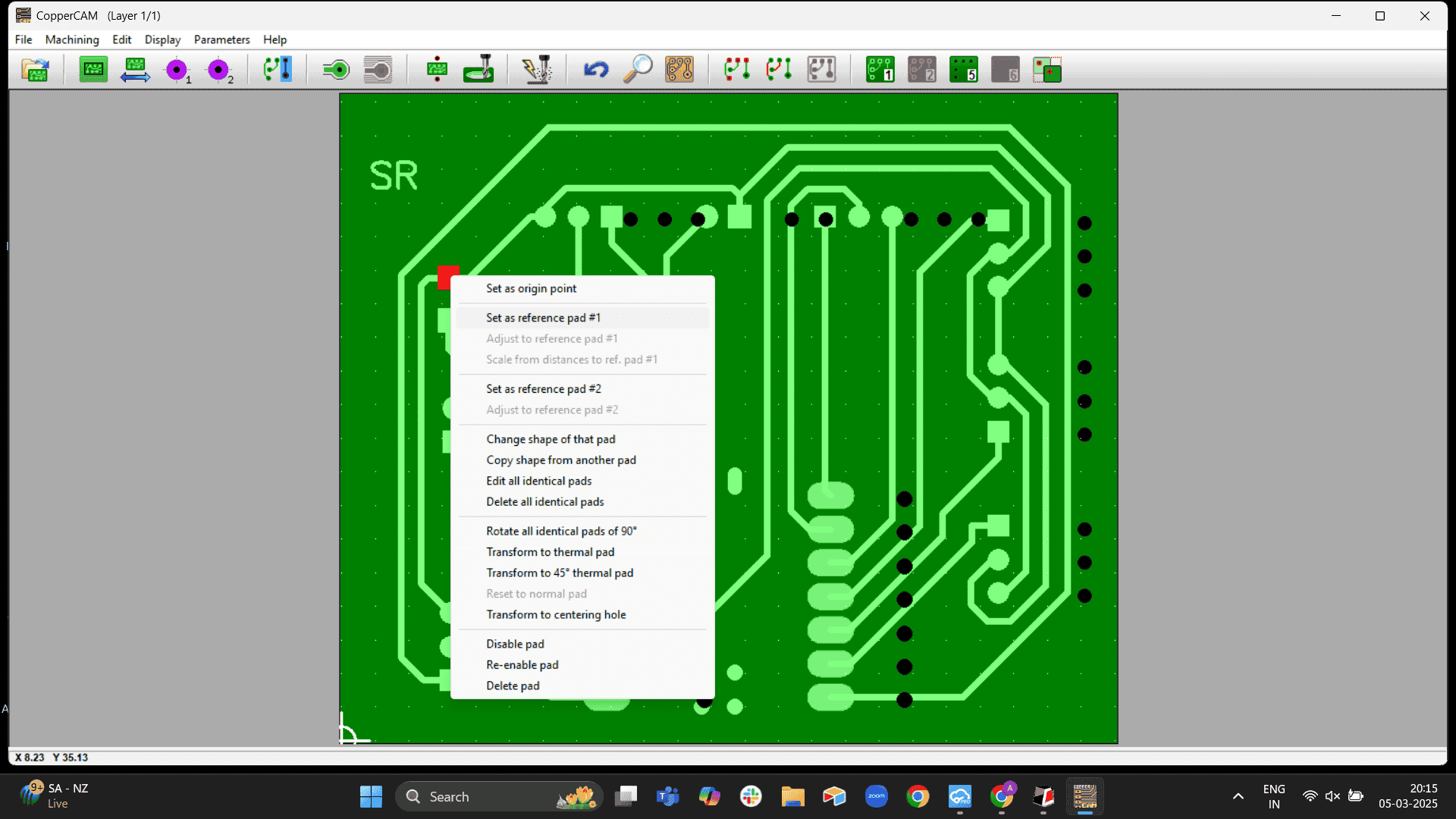
Select on of the pads from the engraving layer> right click> set it as reference pad
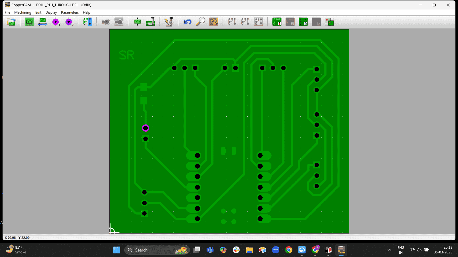
Select the the hole concurrent to the reference pad.
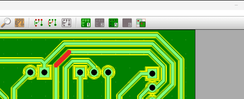
Now on the right top layer you will find two layers> 1: engraving layer and 2: drilling layer.
Calculate countours.
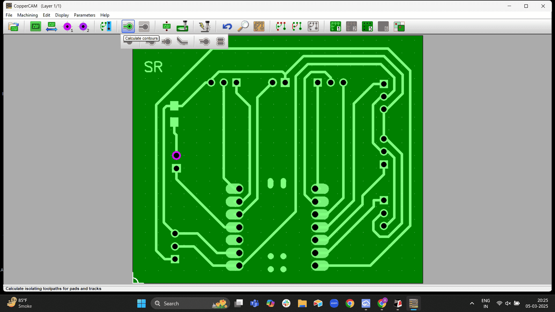
Number of successive conoturs> Set to 5
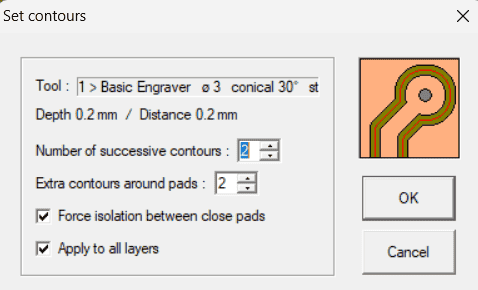
CopperCam interface
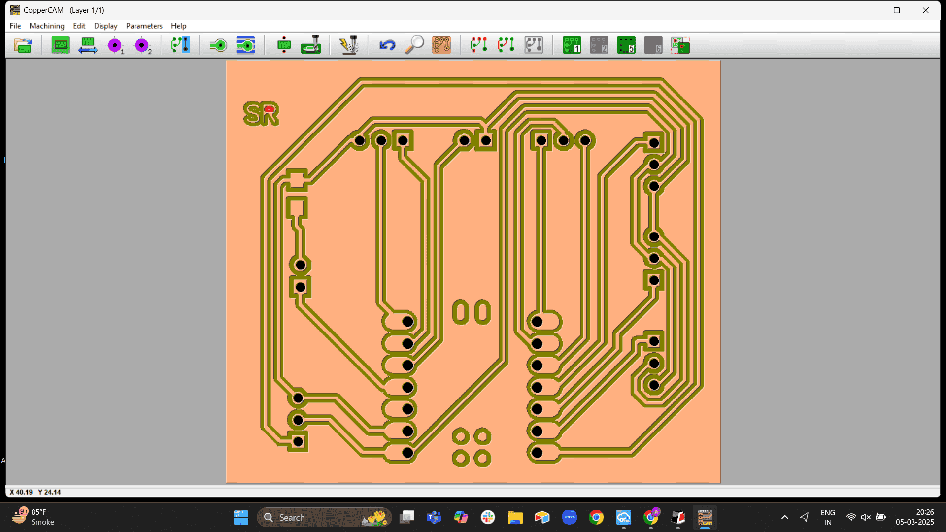
Learnings: I set the successive contours to 2. this made my contours layers very thin
as a result of which, I faced a lot of difficulty while soldering.
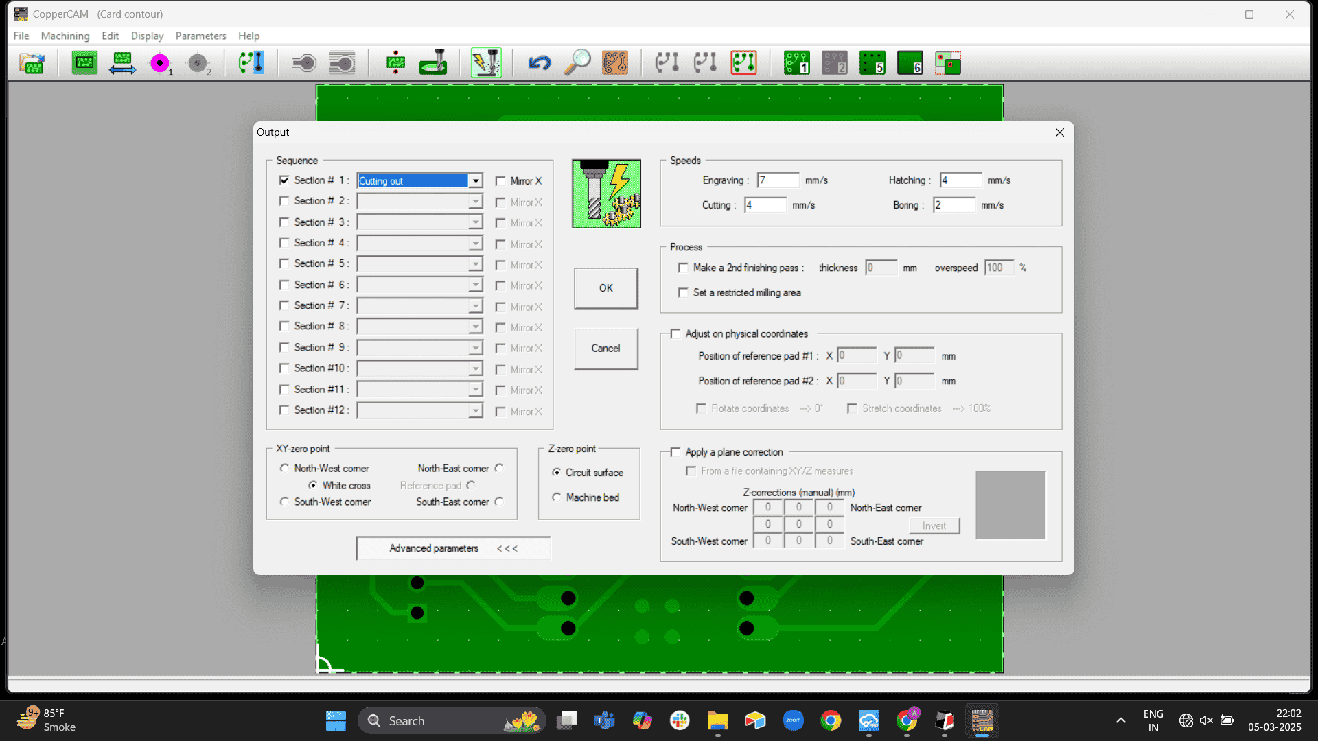
Go to the higlighted icon in the bg> in the section 01 drop down> Engraving layer 1
.png)
Once the Engraving layer is complete we go to drilling

Finally, when the drilling is complete we go to cutting.

As the option differs on every desired output like engraving, drilling and cutting. Other
settings are, XY-xero point set to white cross, this is the origin point we set previoulsy.
Z-zero point as circuit surface as to cut from base and finally "OK" when we have set the
machine axis using the V-Panel.
This is how the PCB will look after production.

Machine run
Hardware Setup:
Power ON the SRM-20.
Connect the USB cable from the SRM-20 to your computer.
Use the square USB-B port on the machine side and USB-A on your computer side.
Wait for the machine to make a small homing sound – this indicates it's powered and recognized.
Machine is set as per the process above

Close the lid for precautions and hit "OK"
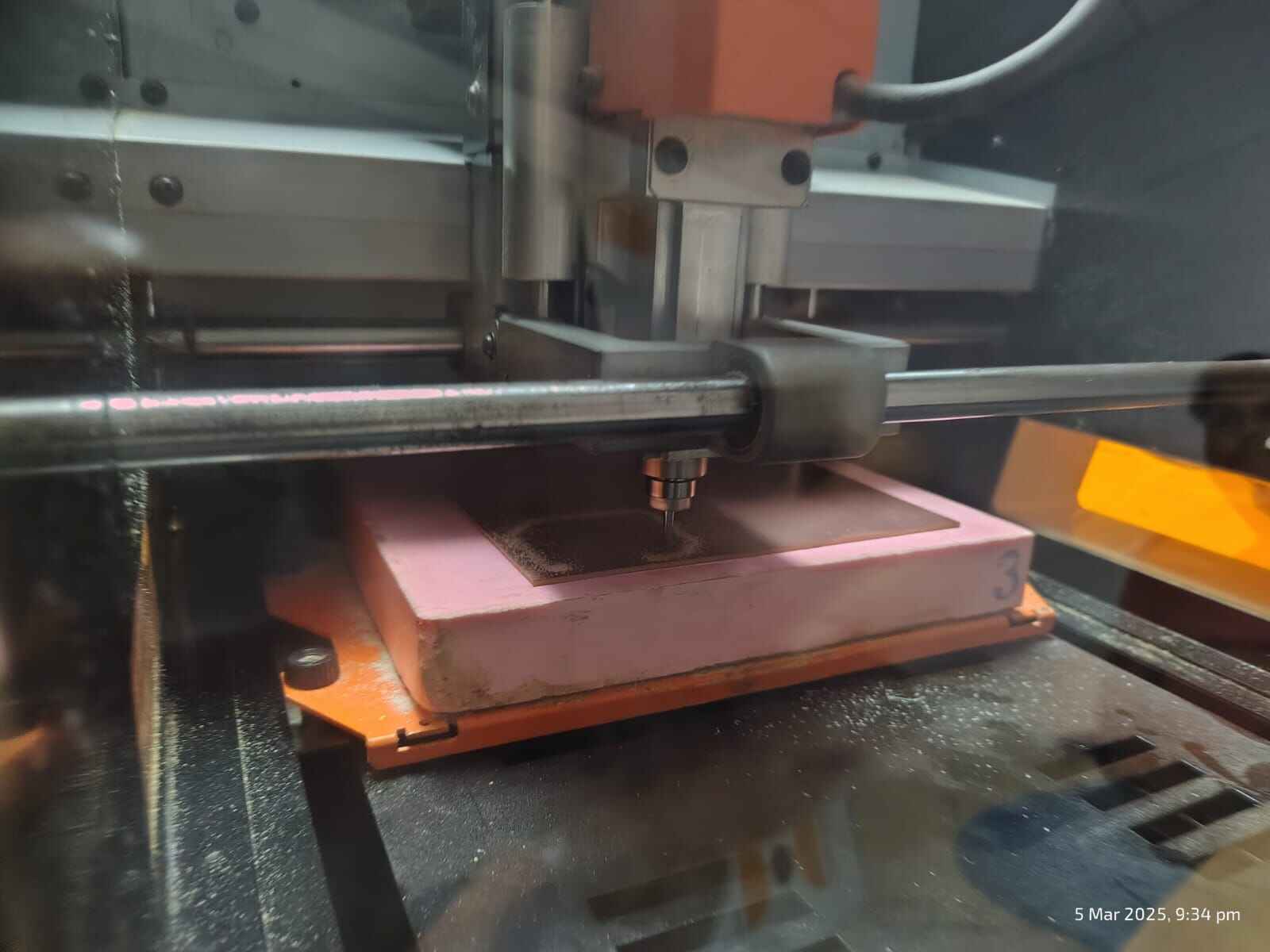
Once the engraving layer is done>
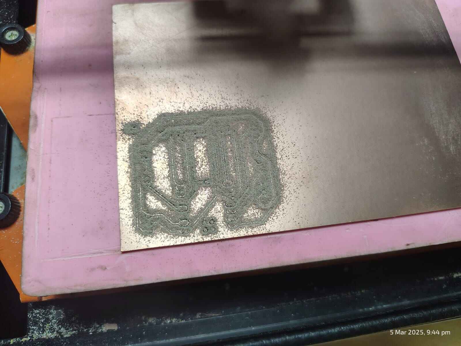
Use a vacuum to pull out the dust.
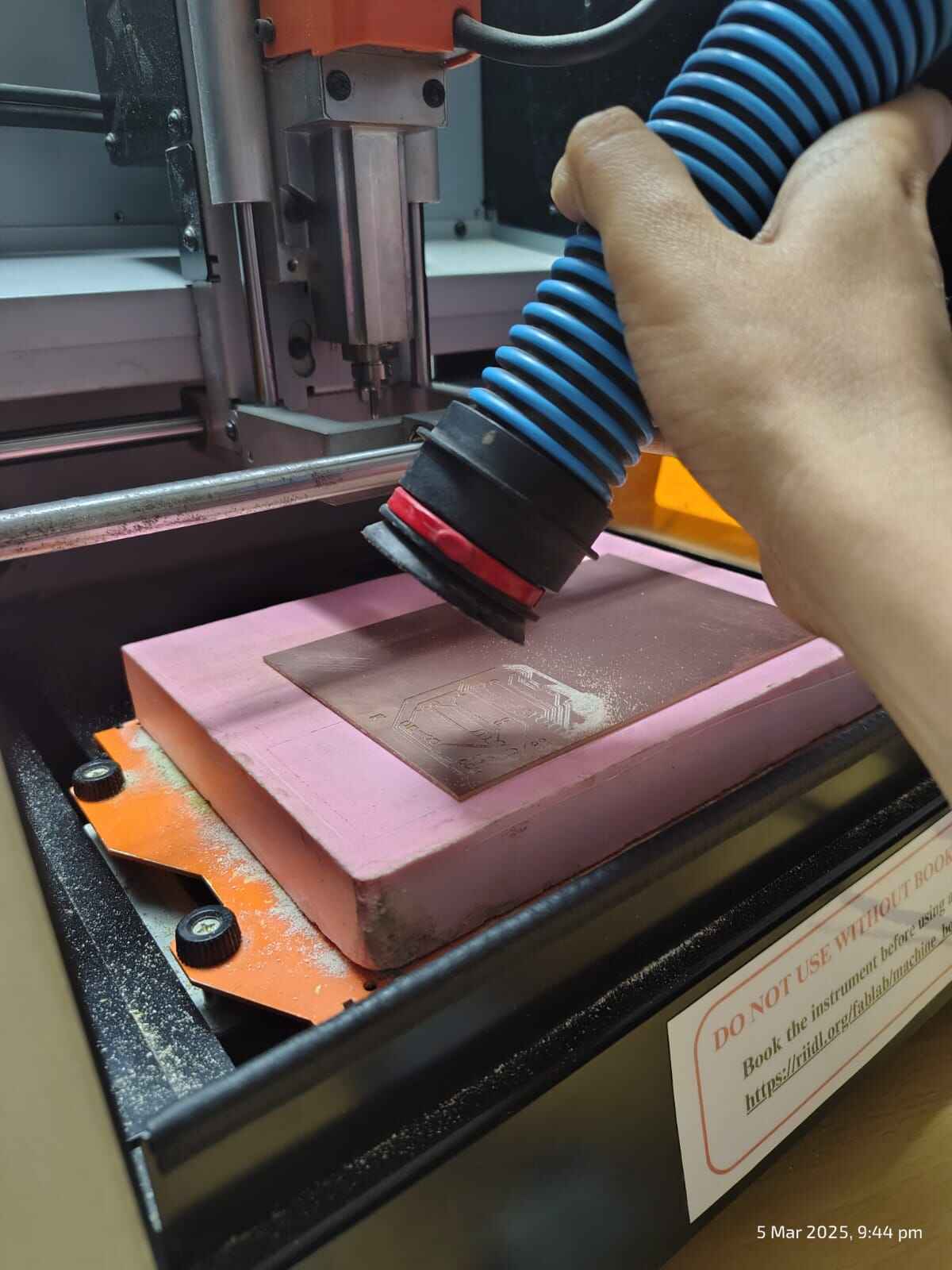
Once the engraving layer is done, we will have to change the tool bit for drilling and cutting the corners.
For which firstly, we more the X and Y co-ordinates of the tool path away from the board using the V-panel.
Make sure that the " Set origin Option" is untouched. Now on the SRM-20, change the output sequence to cutting>
and cut.
Once the Drilling and cutting layer is done>
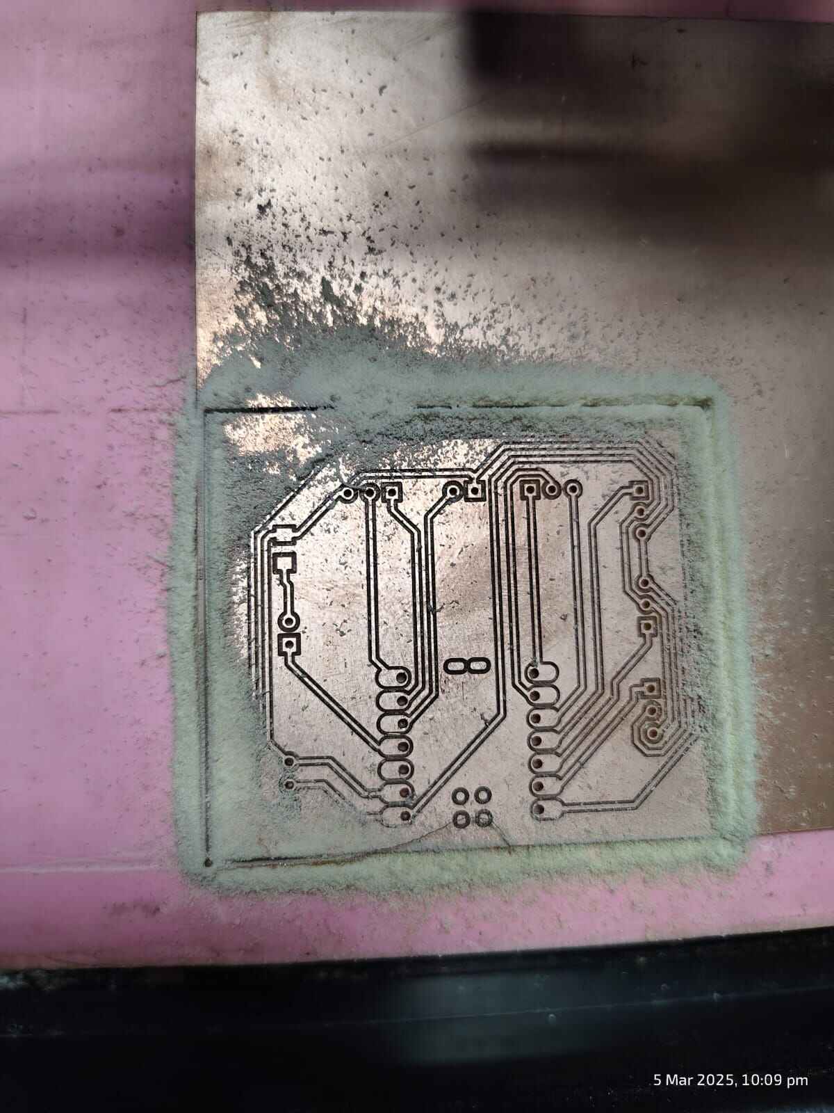
Use a vaccum to pull out the dust.

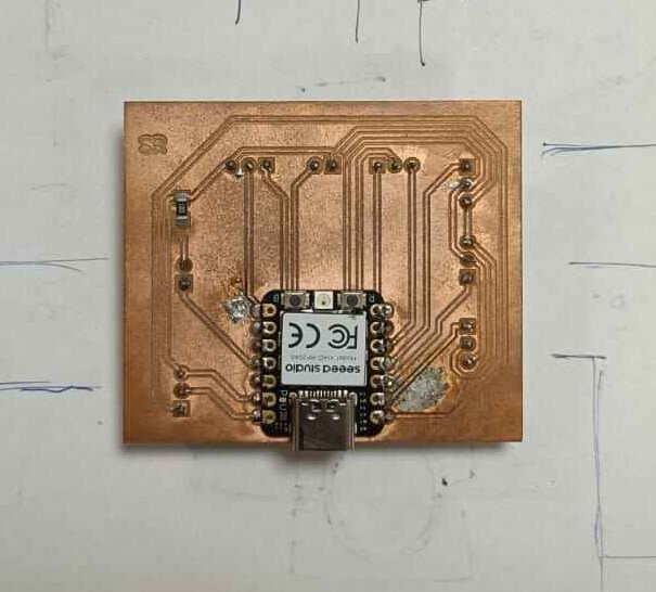
First Ever Milled PCB! Exclaims,"Wow!"
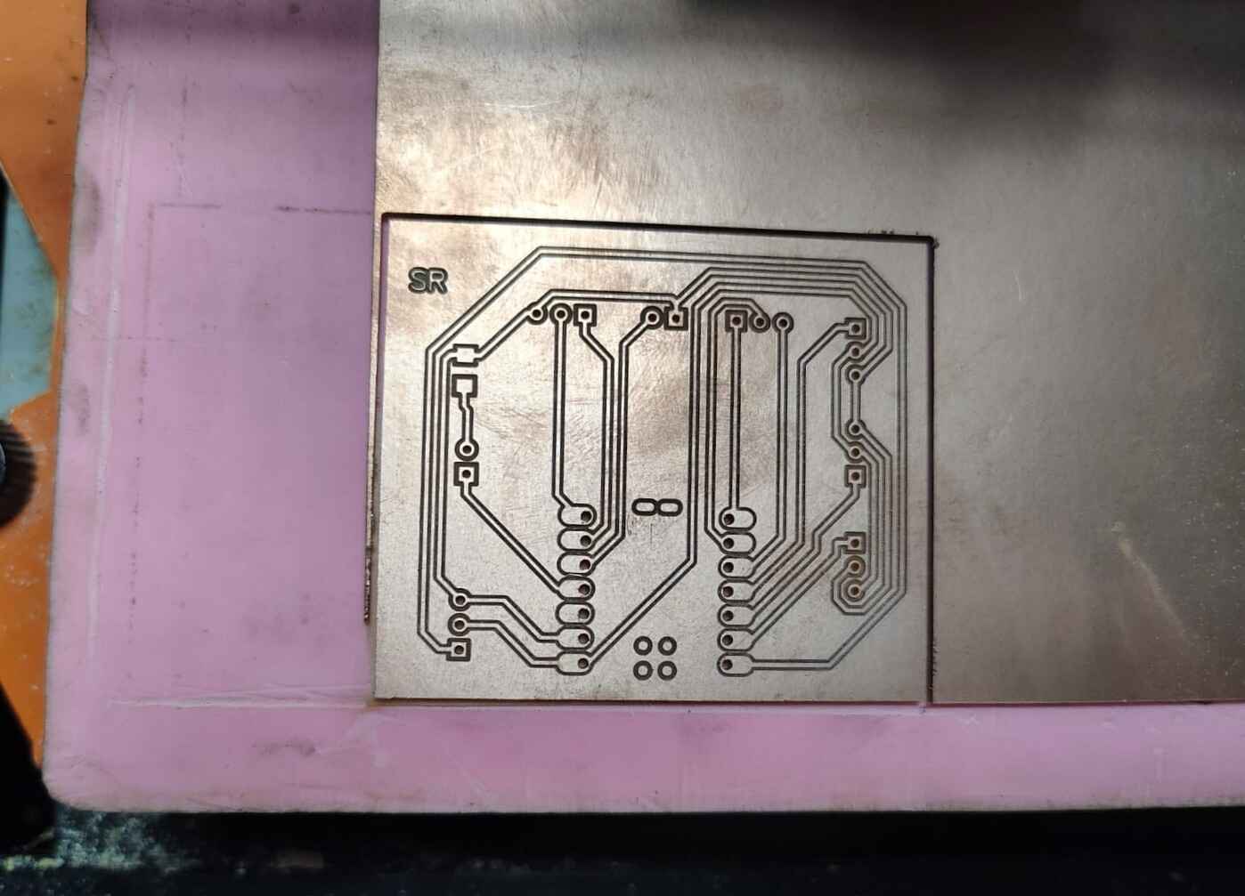
Hero Short: 2
.jpg)
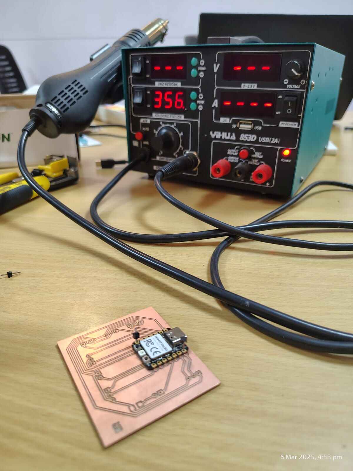
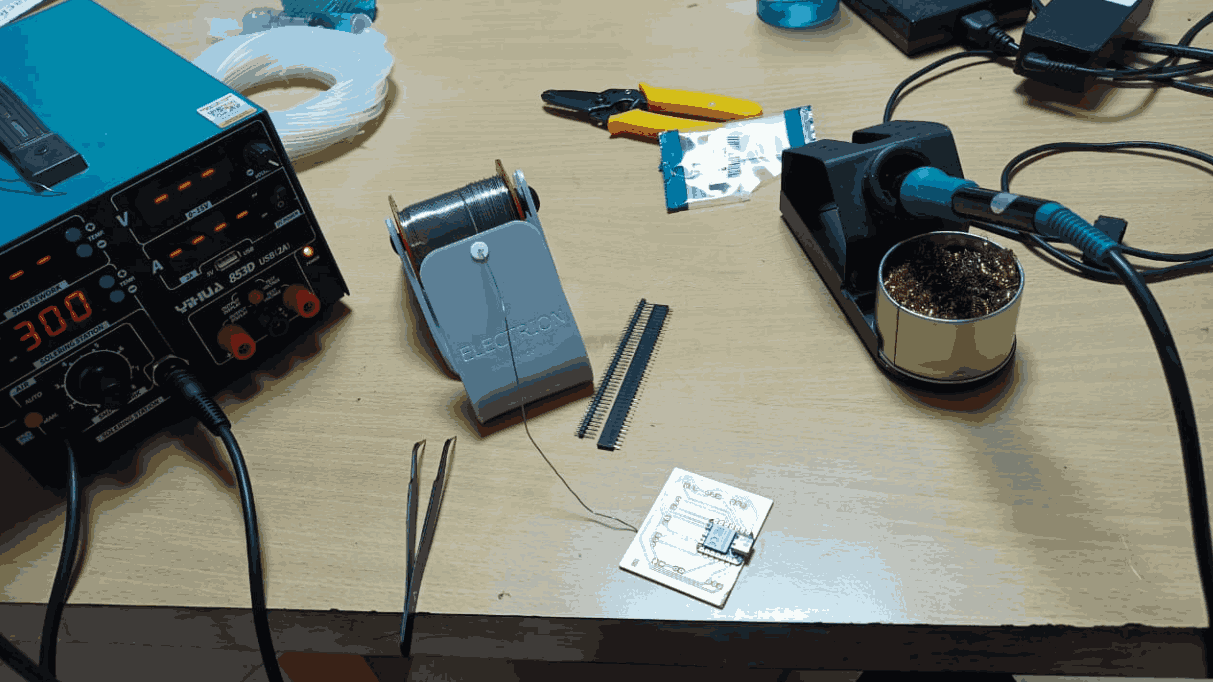
Soldering AND Debuging!!!
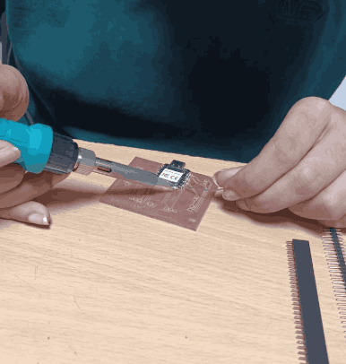
Soldering

And more soldering.

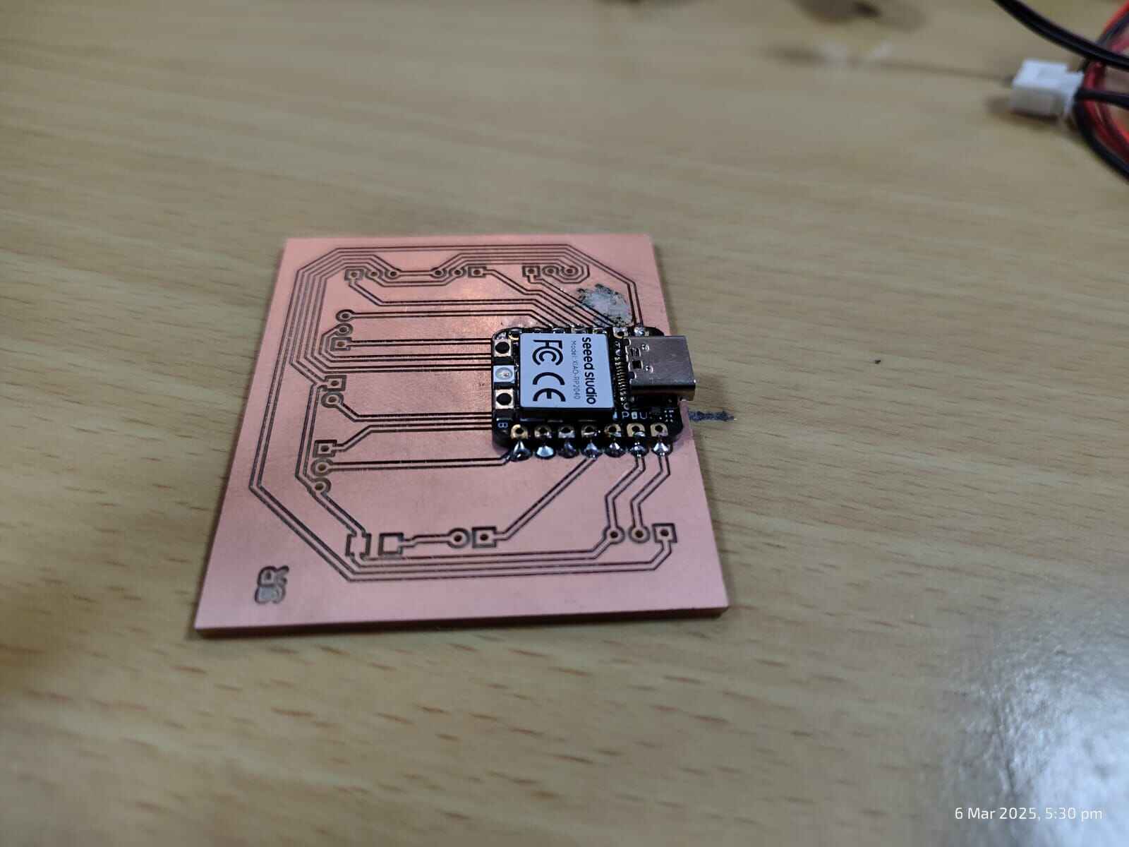
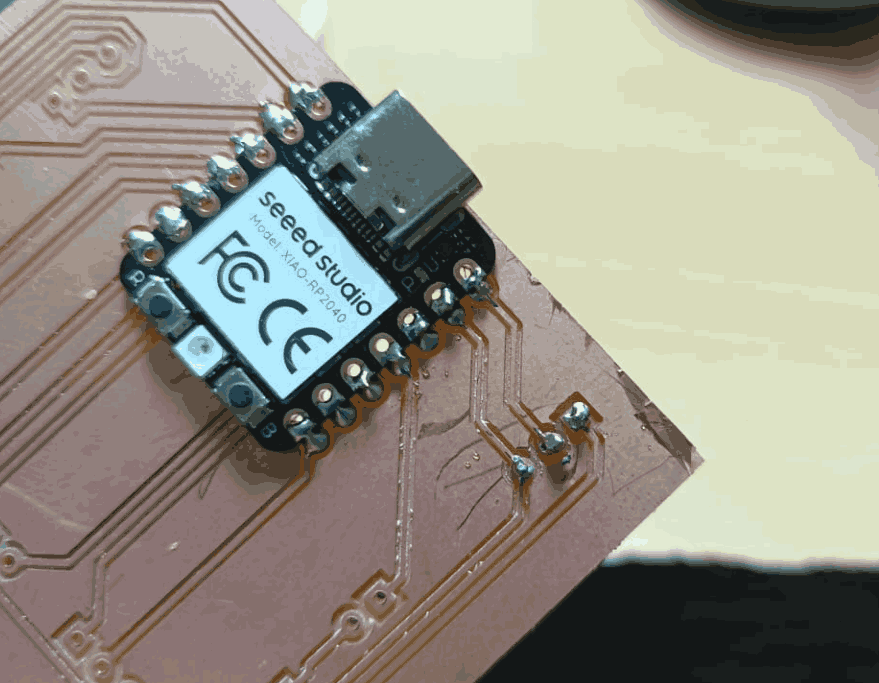
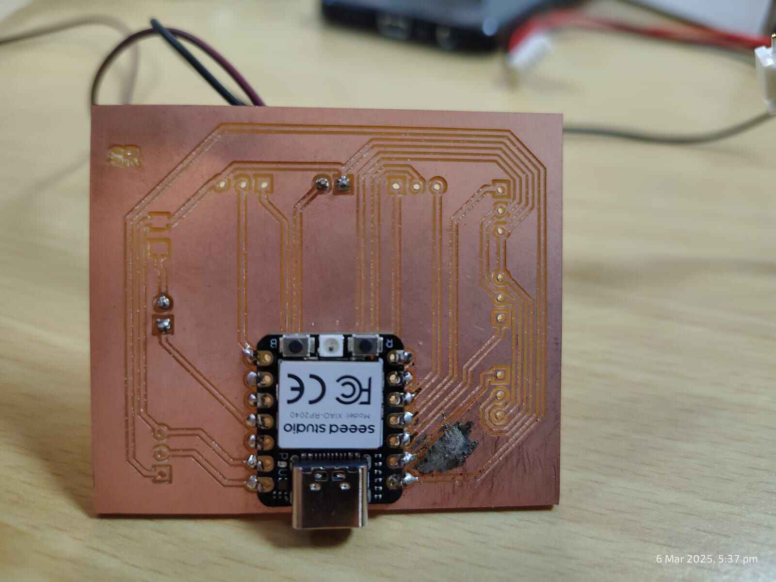
Learnings: As I mentioned the countours that I set for the track was only 2, due to which the souldering process
became very
tough for me. The attention required to solder the XAIO board to the PCB, moved to not letting the soldering wire
stick to the board excess copper wire. As a result of which,
as I am new to soldering, some soldering wire got transferred to the copper plate which led to a mis-connection.
Here, I used a suction pump for desoldering.
to get rid of the mis-connection.
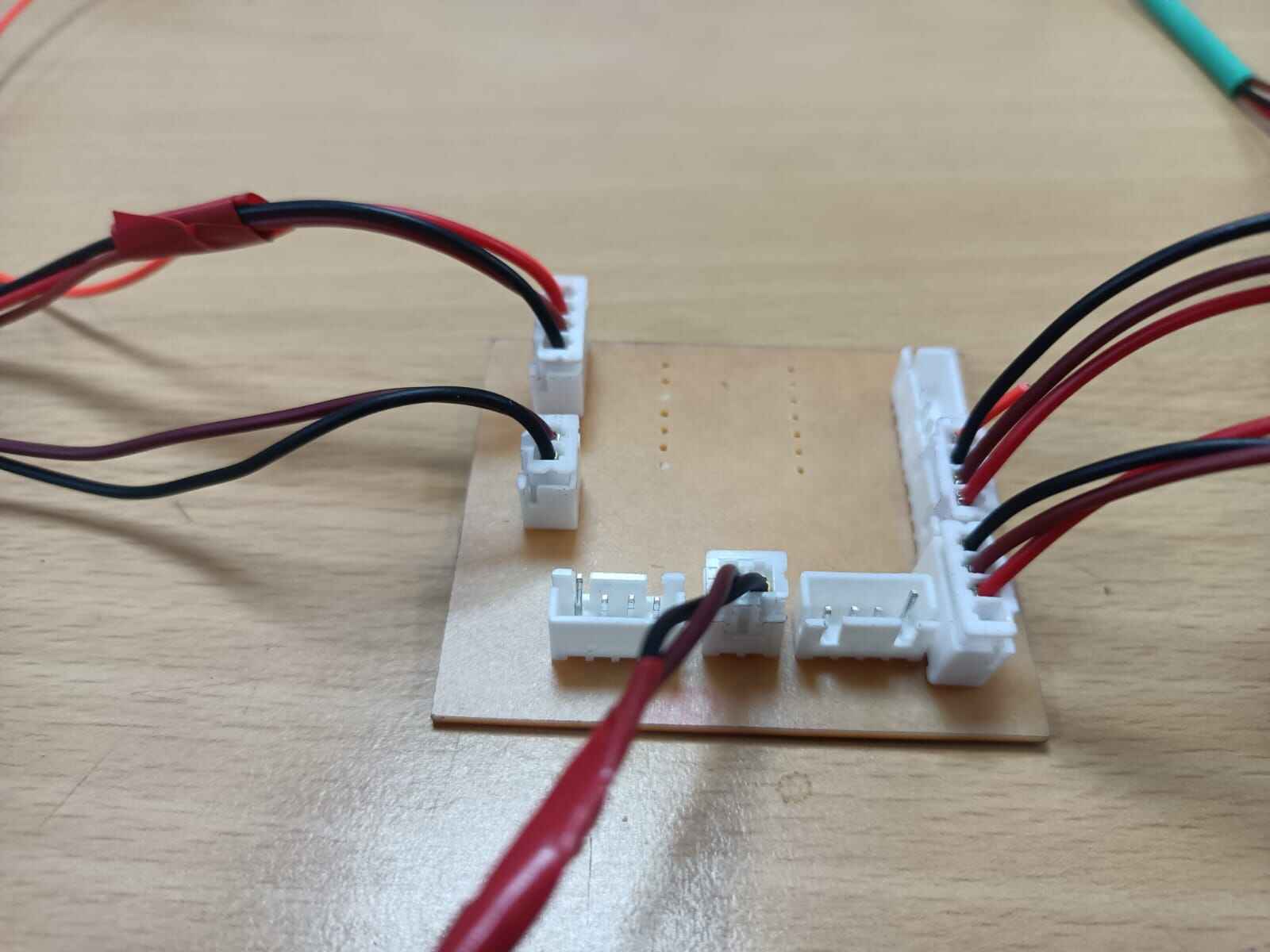
Soldering other elements. That is the JST pins.

JST Pin connection.

Process:

Process 2:

Soldering other elements. That is the JST pins.

JST Pin connection.

Note: The reason why I used an JSt pins as in through holes for soldering is by keeping in mind my Final Project.
This PCB will be connected to elements like Servo and DC motors which will be farther away from the Board.
Plus, there is going to be another PCB with SMD LED's on which will be connected to this board. I performed the
complete
soldering process in the week 04 of my documentation. To learn more about soldering, refer to the
Week 04: Embedded Programming
of my Documentation.
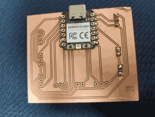
Post soldering all the JST connections through a through-hole soldering, along with an SMD soldering resistor.

Debugging
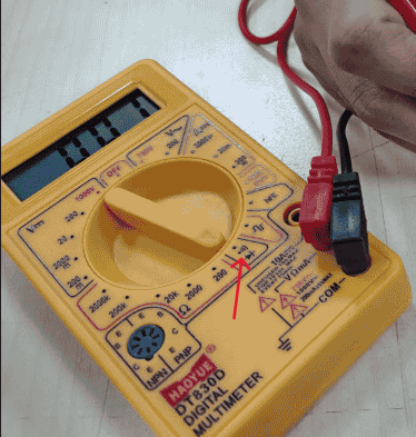
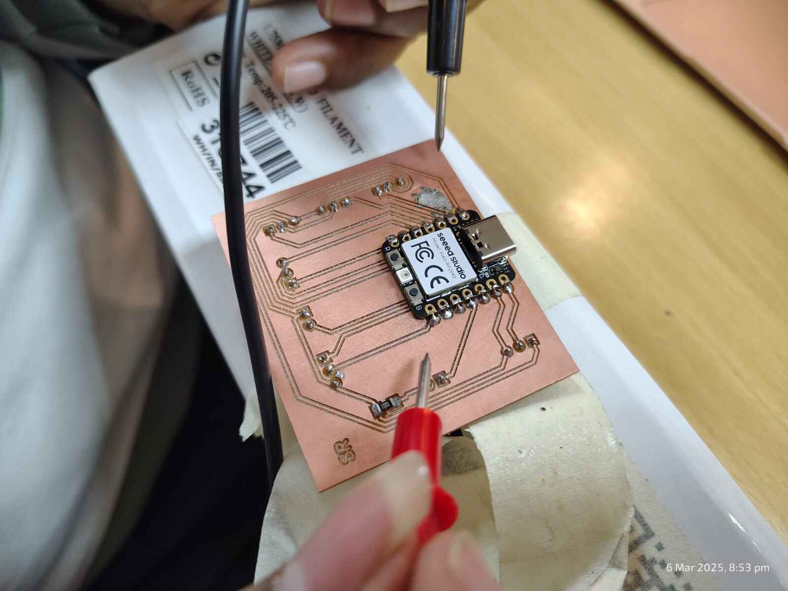
Using a Multimeter to check if all the connections are working proper.
How does the Mulitmeter work?
For the connectivity symbol the multimeter will help you check the connectivity between two linkages.
Wehn two points with connectivity are touched upon buy the multimeter, red and black pin wires, the number >0
signals
to connectivity ans will give a beeping sound output.
Pull the dial to the: connectivity symbol.

Used the multimeter to check every point of connections refering to my schematic.

Testing
Used the multimeter to check every point of connections refering to my schematic.
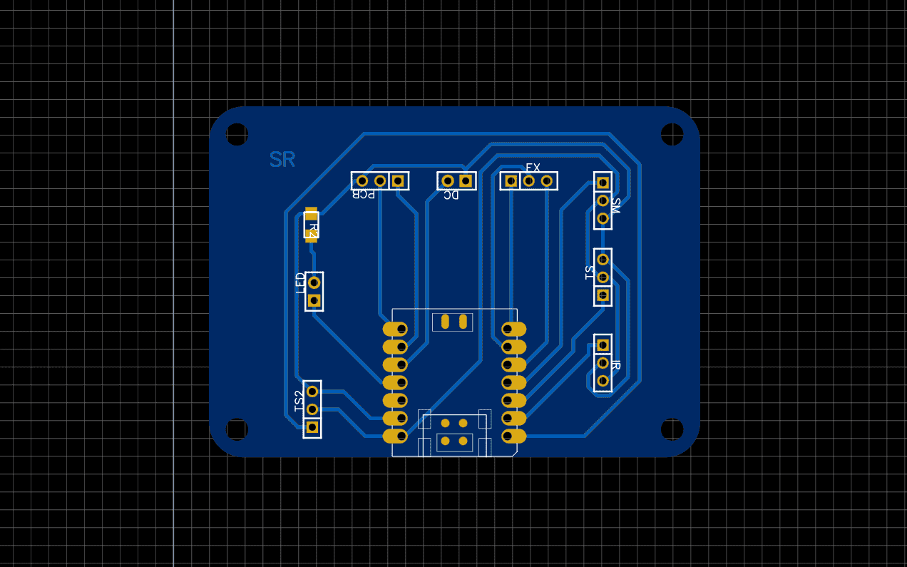
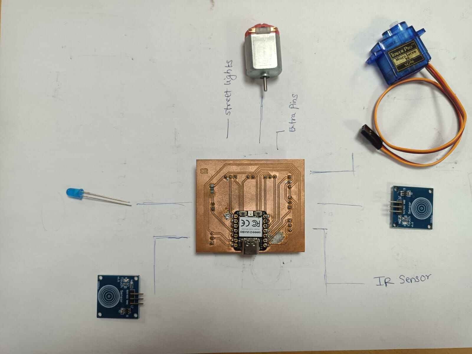
Referring to my PCB Schematic to learn the position of every componenet that needs to be soldered to the JST
pin wires.

Referring to my schematic and build a live schematic for my understanding.

Now soldering the JST pin wires to the pin wires to the target components. A very big learning here was the
mirror effect.
As we PCB mill on the top surface, the through holes on the back surface become the mirror image of the above.
Thus, if the 5V of a 3 Pin Jst wire is the top.
It will move to the buttom because we have gone to the bottom surface which is the reverse of the engraving and
drilling side. As I was using only JSt pins the
over connections didn't make a big difference but I had to contantly turn over and check the wire configuration of
my Easy Eda Circuit to solder the 5V pin hole of the
PCB to the 5V pin of the Servo.
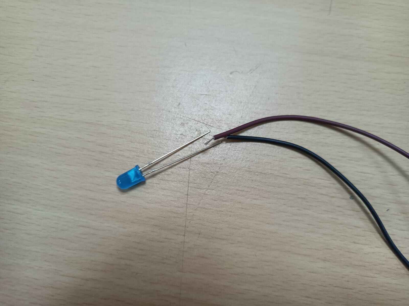
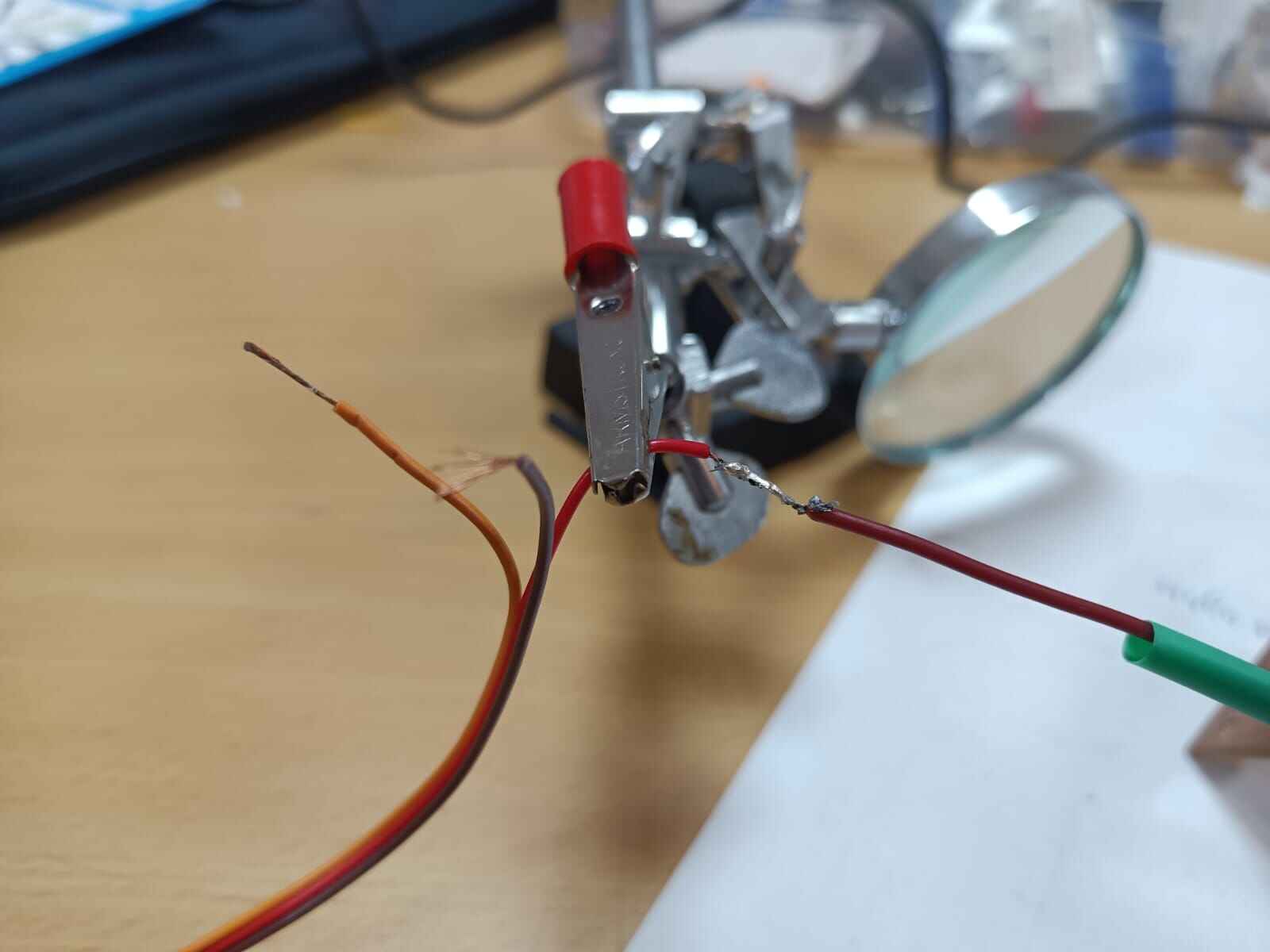
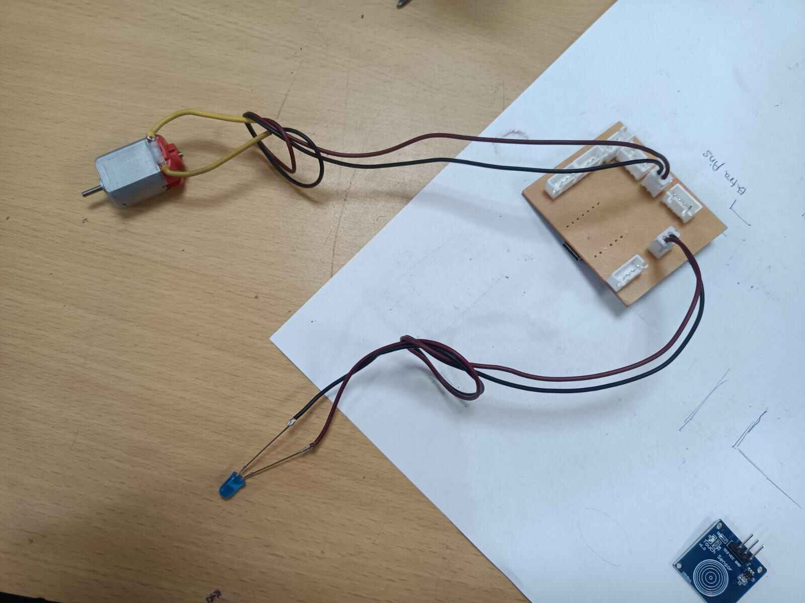
Soldering the wire to the LED. Firstly, I checked the positive and the negative of the LED and wire
and soldered it respectively.

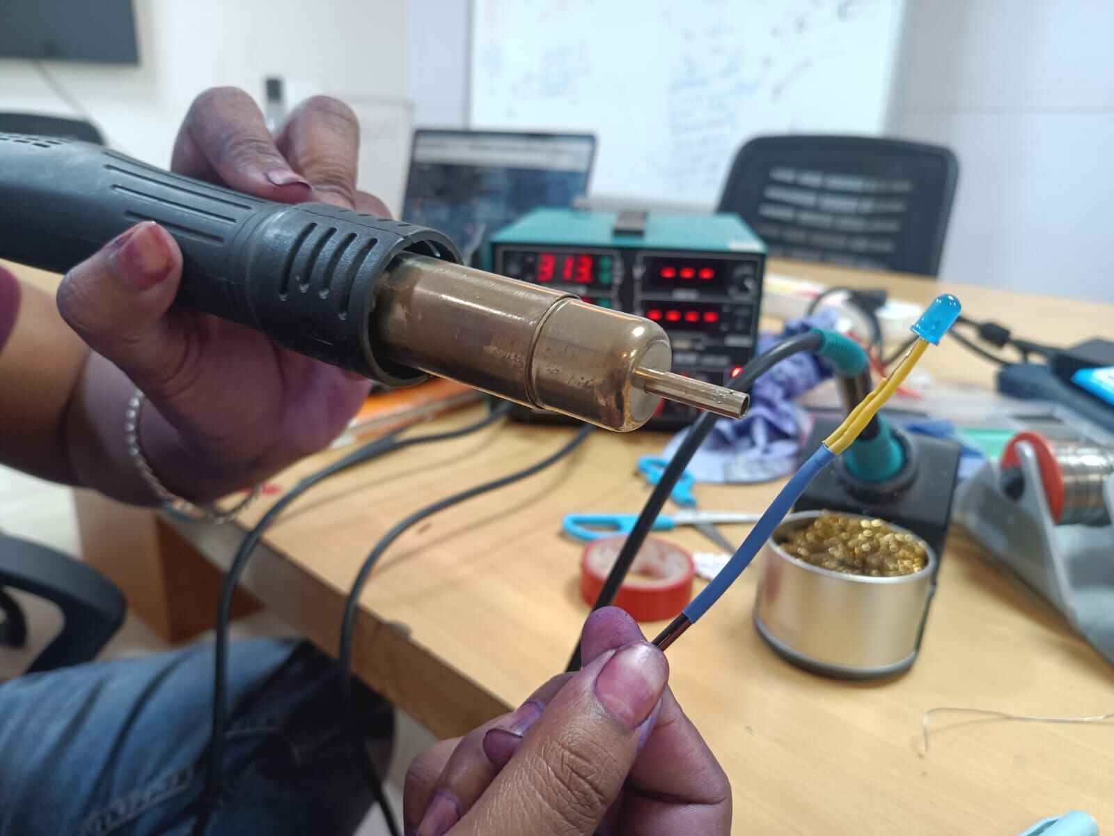
I used a Wire Stripper to remove the copper around it. Now wrapped the wire aroung the LED and soldered it

Before soldering, I also put a heat shrink tube about the wire and once soldered, using Rework Station shrink
the tube by heating it.

In the similar manner I soldered the DC Motor.

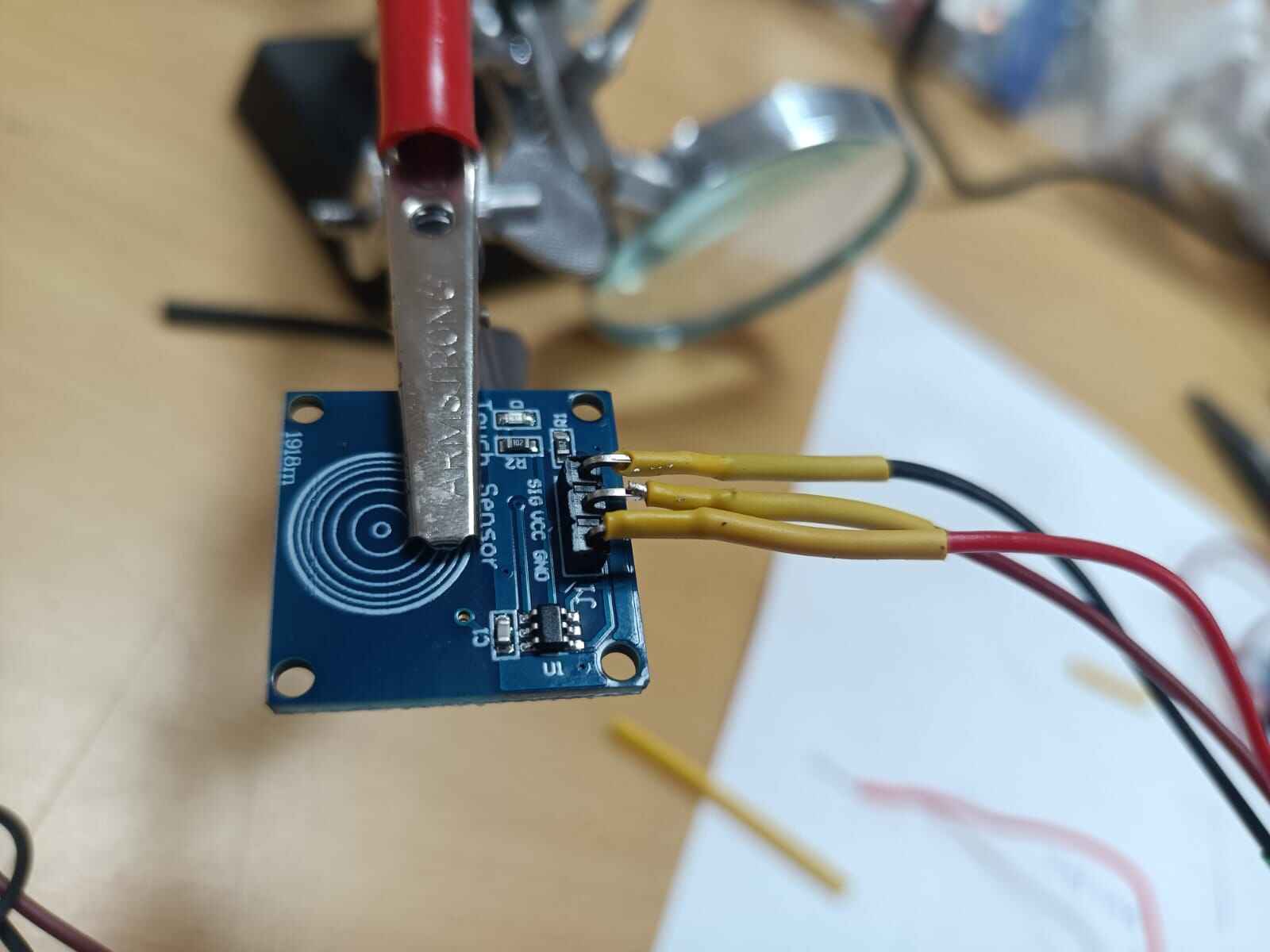
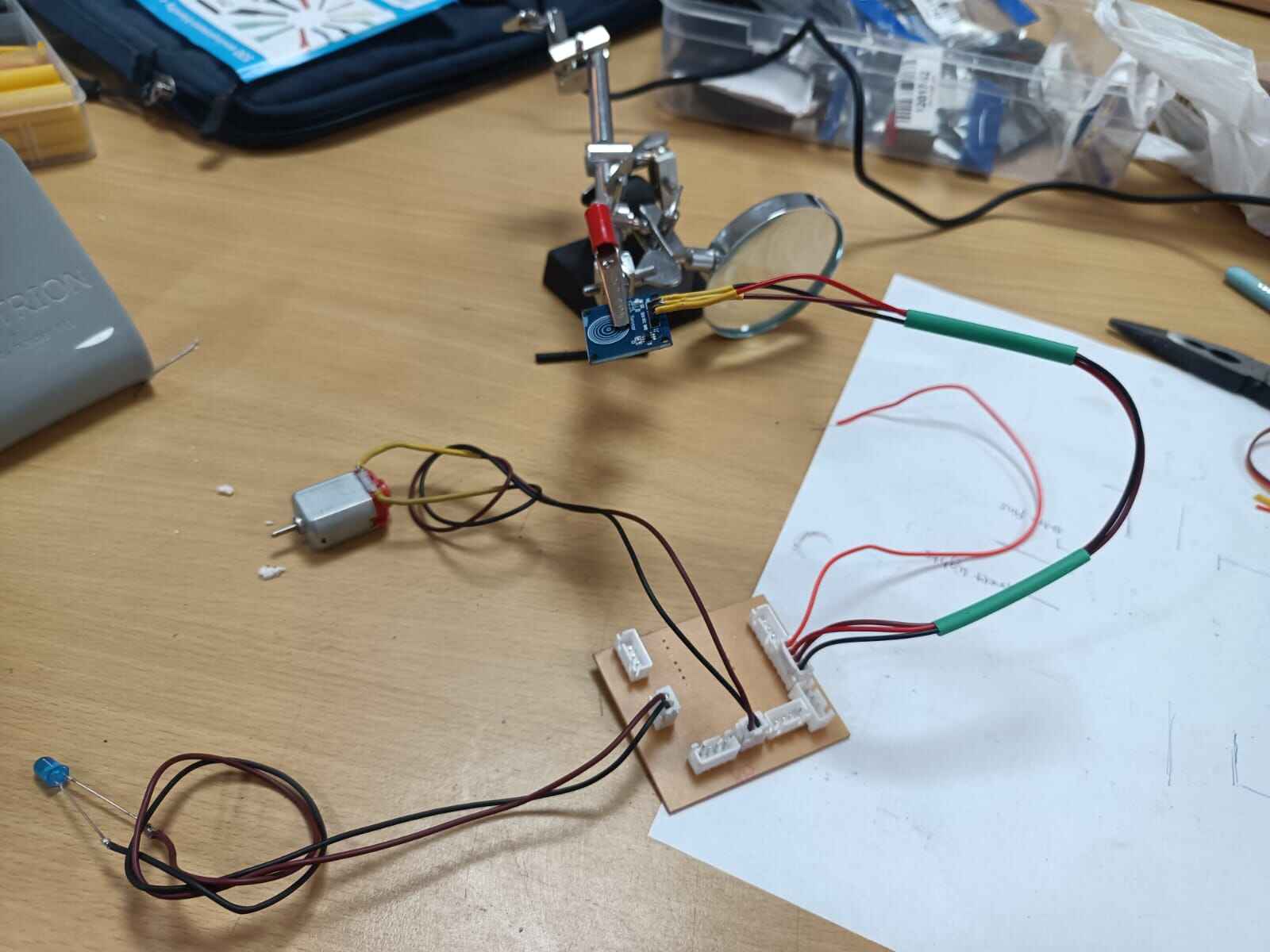
Soldered the Touch sensor as well.

Emphasizing here to check the pin configuration as per the PCB design.

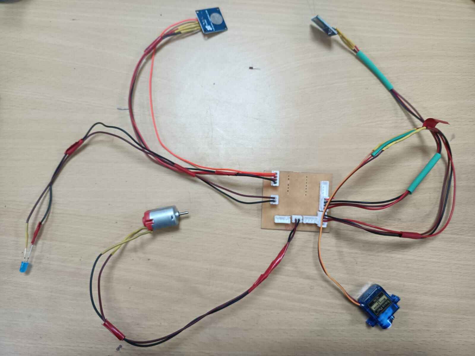
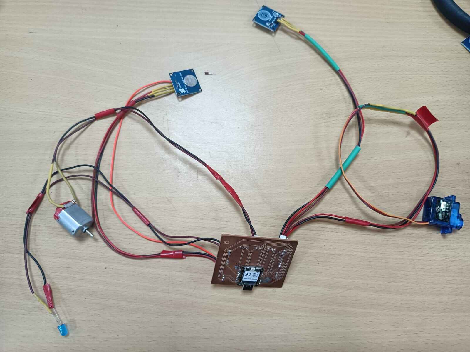
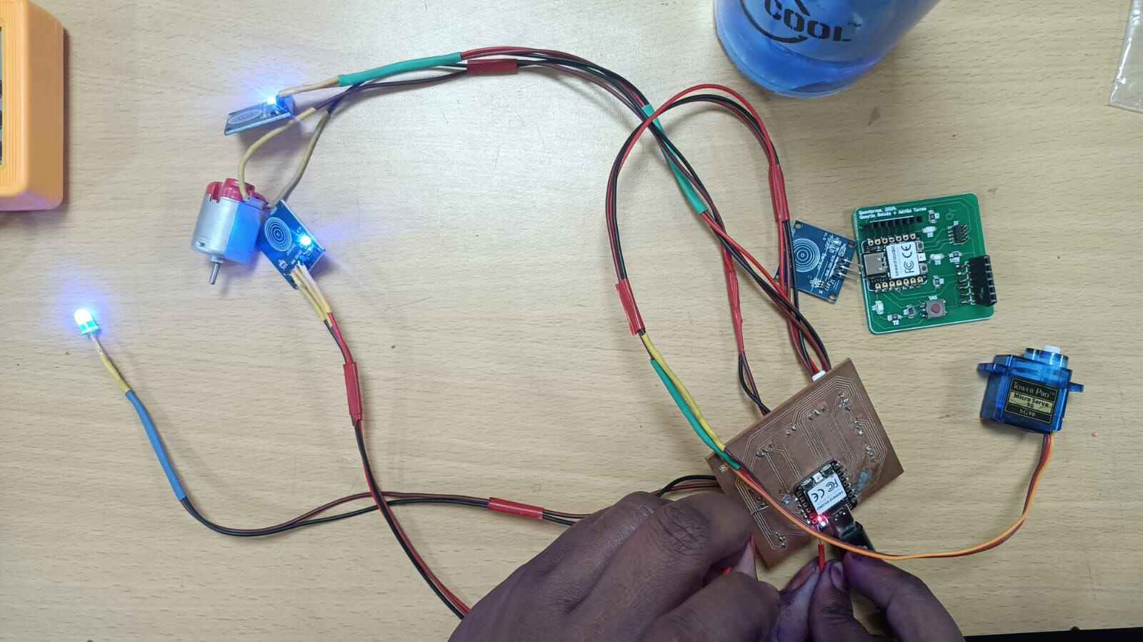
Assembled of all Products

Soldering of all devices.

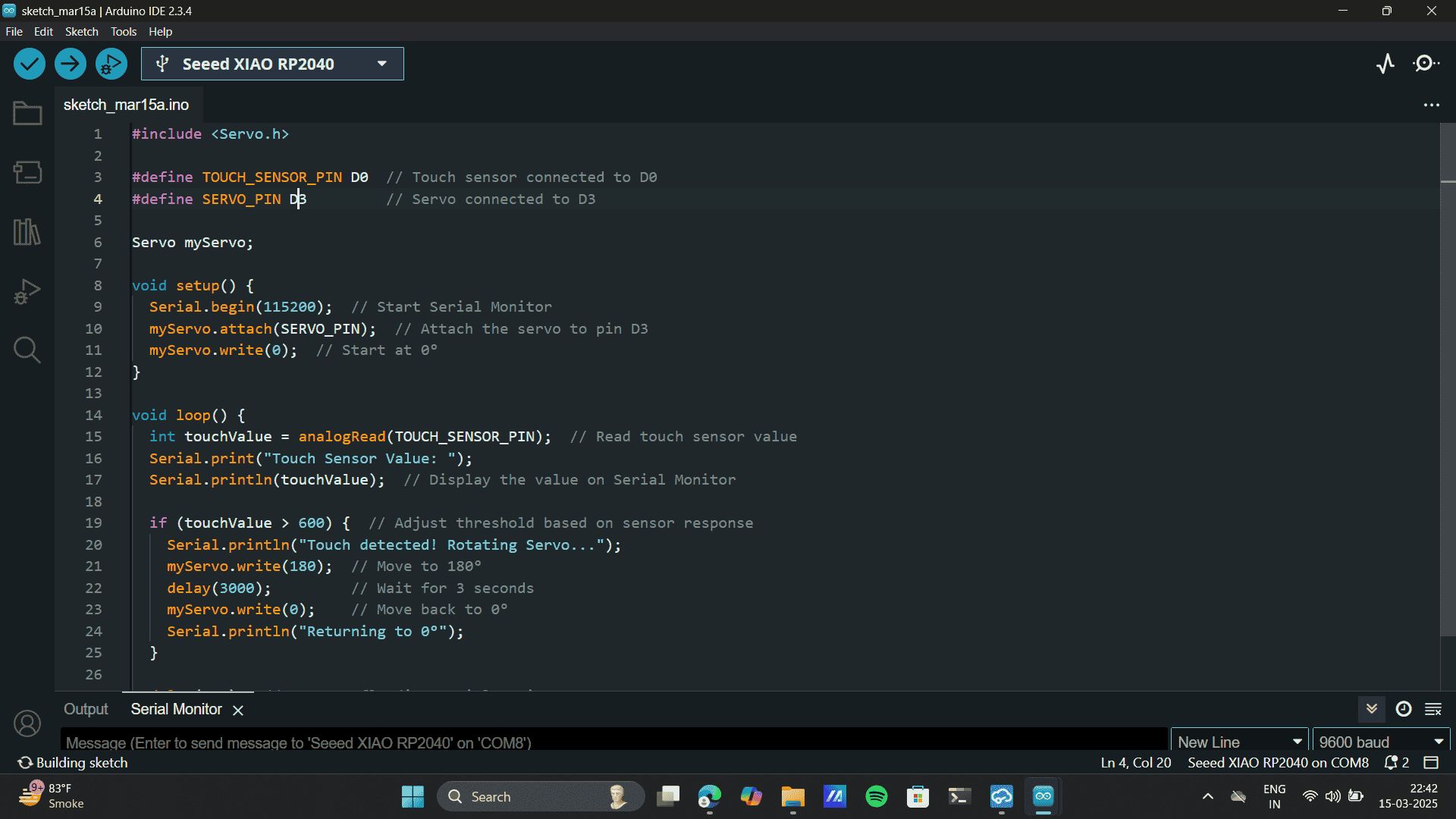
Ran the code for which I partially used AI

Final tested the working of the board

Learnings:
hrough designing, fabricating, and testing my custom microcontroller development board for the final project, I
gained hands-on experience with PCB design, component selection, and circuit layout. I learned how to route traces
efficiently, ensure proper power distribution, and follow design rules for fabrication. Assembling and testing the
board taught me the importance of debugging techniques, checking connections, and verifying functionality with
firmware. This process gave me a deeper understanding of hardware development and boosted my confidence in
creating custom embedded systems from scratch.
Group Assignment
Check out this week’s Input Devices group assignment on Mihir's documentation site
here
I learned to characterize the design rules for in-house PCB production by testing parameters like feed rate,
speed, plunge rate, and cut depth. Using Adobe Illustrator to create the design and exporting it as an SVG helped
me understand the role of vector formats in PCB design. In EasyEDA, generating Gerber files gave me insights into
the digital fabrication process and the importance of precision in machine-compatible designs.
We realised that the best output that our machine gave was at 0.5-0.6 clearance.
Project file
Code file
Gerber file
Gerber file 2
Image Links
Image
Link.
Image Link.
Image
Link.
Image
Link. 


.jpg)
.jpg)


.png)
.png)


.png)


.png)


.jpg)
