6 - Electronics design
In this week, we will learn the importance of electronic design software, which allows the creation of PCB (Printed circuit board) taking
into consideration the "Electrical Rule Check" (ERC) and "Design Rule Check" (DRC) verification processes.
Nowadays there are many designs software, some will be listed below.
- KiCad - PCB design - Free
- Eagle - PCB design - Pay
- Altium - PCB design - Pay
- Cadence - IC Design & Verification (Virtuoso)
- Synopsys - Design, Verification & Manufacturing
- Mentor - Verification and manufacturing of integrated circuits (ICs) and electronic systems
KICAD FIRST STEPS
Before starting it is important to first download the following file.
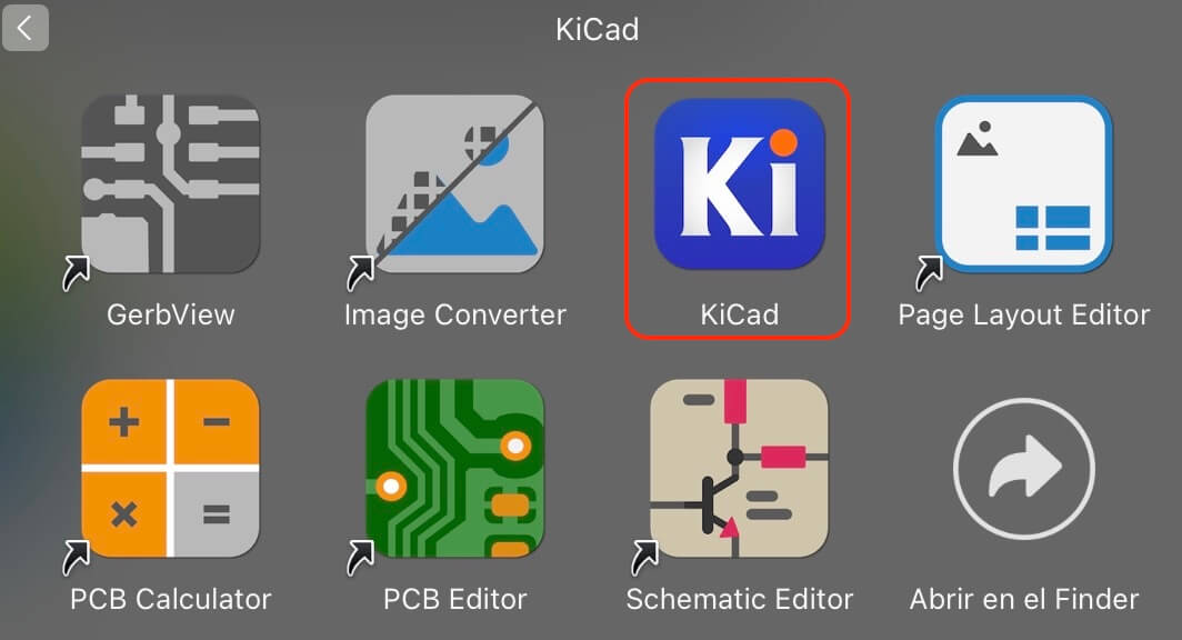
Once " kicad-master.zip" has been unzipped, proceed to open " KiCad"", for MacOs users it looks like the image below.
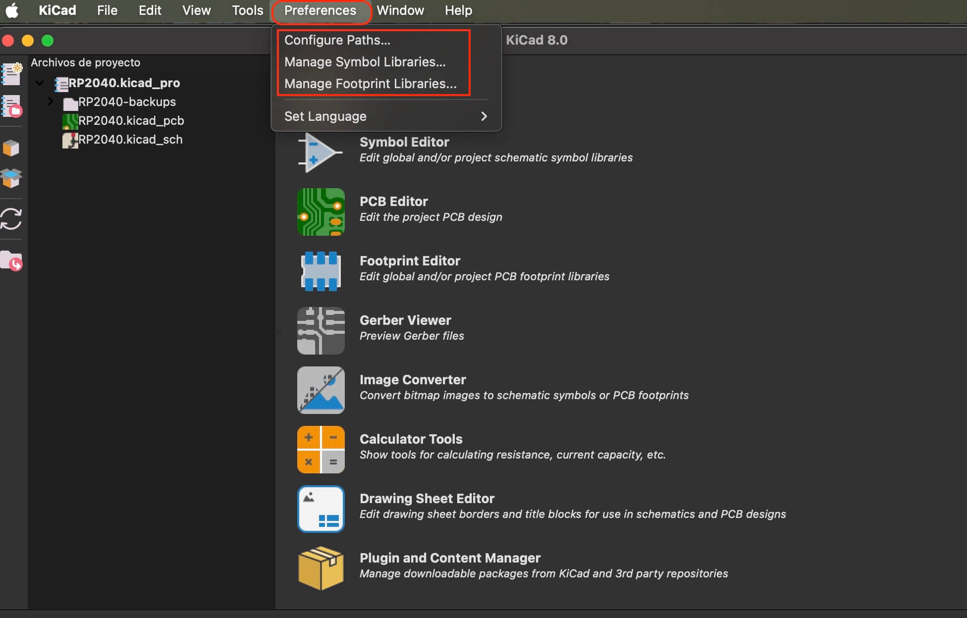
Pressing the selected icon in the image above opens a new window. We go to "Preferences", where we must "Configure Paths" and "Manage Symbol and Footprint".
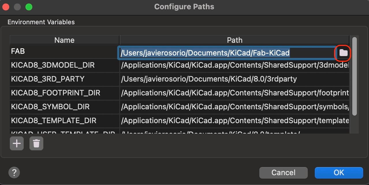
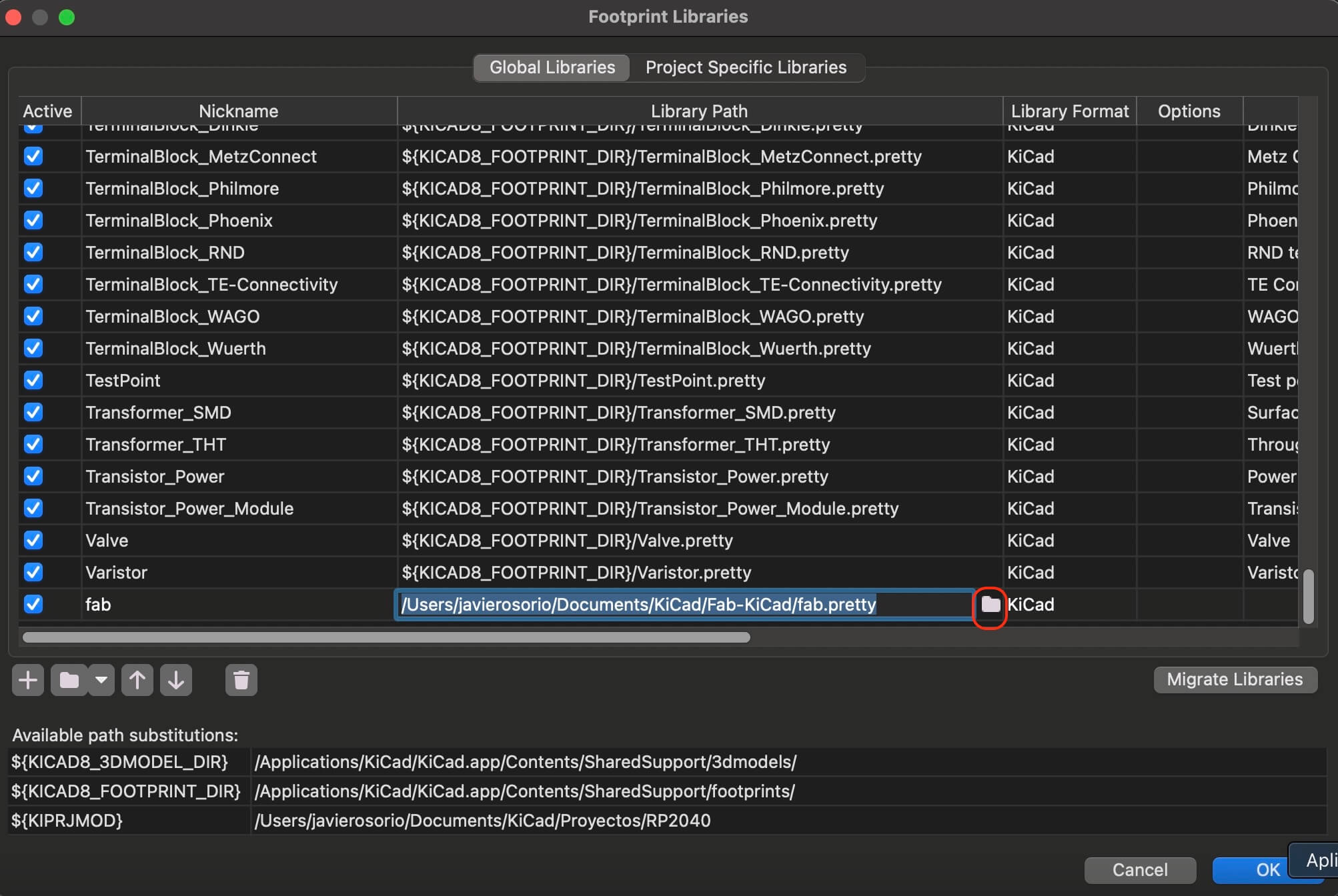
From the "Preferences" menu, we first select "Configure Paths", that will open a new window where we will look for the unzipped " kicad-master.zip" folder, select the "Fab-KiCad" folder and press "OK".
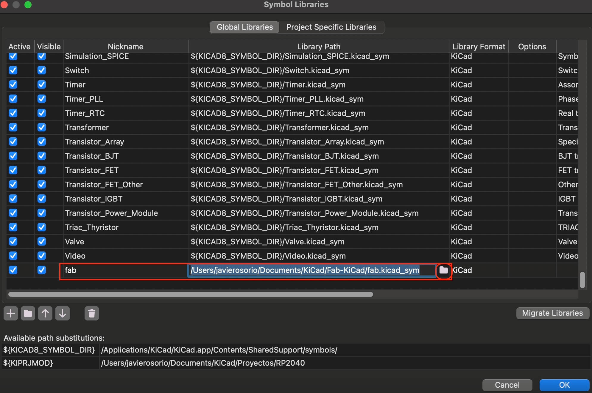
We return to "Preferences", select "Manage symbol" and from our unzipped folder we look for the "fab.kicad_sym" file.
The last step of the configuration is from the "Preferences - Manage Footprint" menu, look for the file ending in "fab.pretty", press "OK".
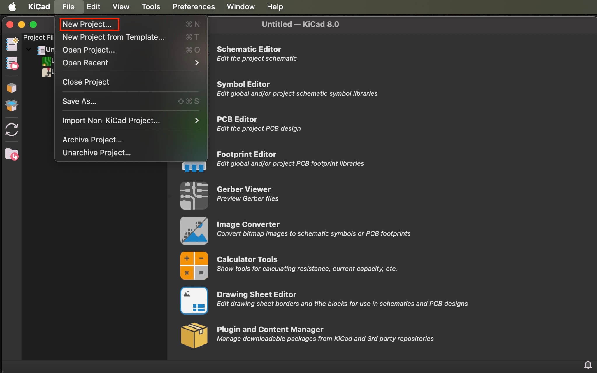
Once the previous steps are finished, we can start working with "KiCad", the first thing is to open a new project.
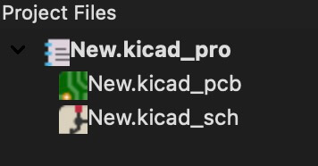
When creating the project, the project files appear, which are the "Schematic Editor" and the "PCB Editor".
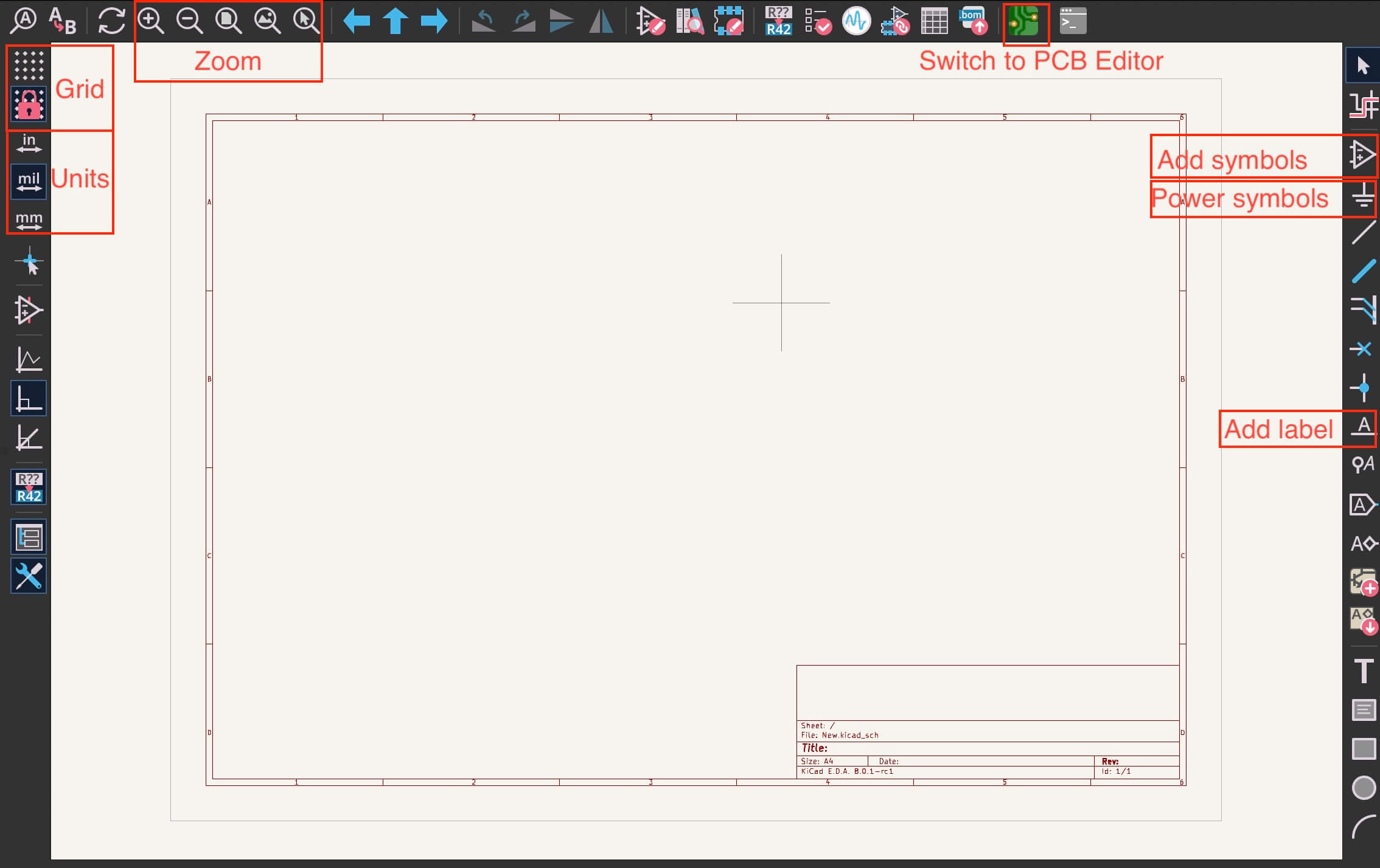
First, we open the "Schematic Editor", which is where the schematics will be made, which once finished we continue to go to the "PCB Editor". In the Schematic Editor window, we can identify a series of icons on the periphery of the work area; some of the most important ones are shown in the figure below.
On the other hand, "PCB Editor", which is the space where the layout will be carried out, has some important icons that are shown below.
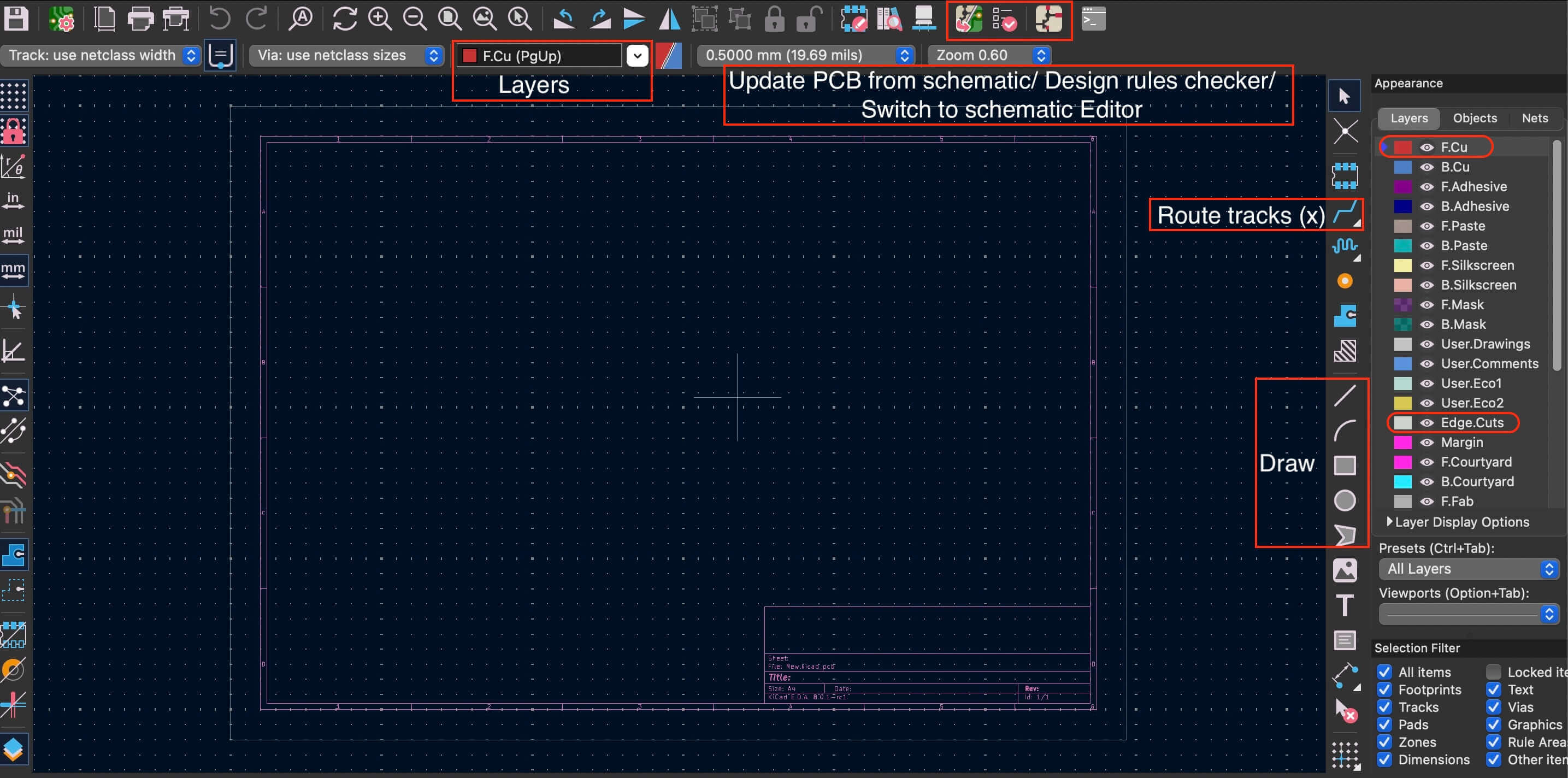
Schematic Editor
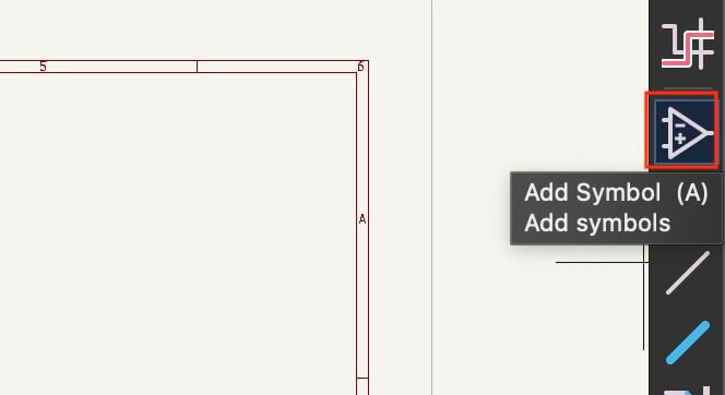
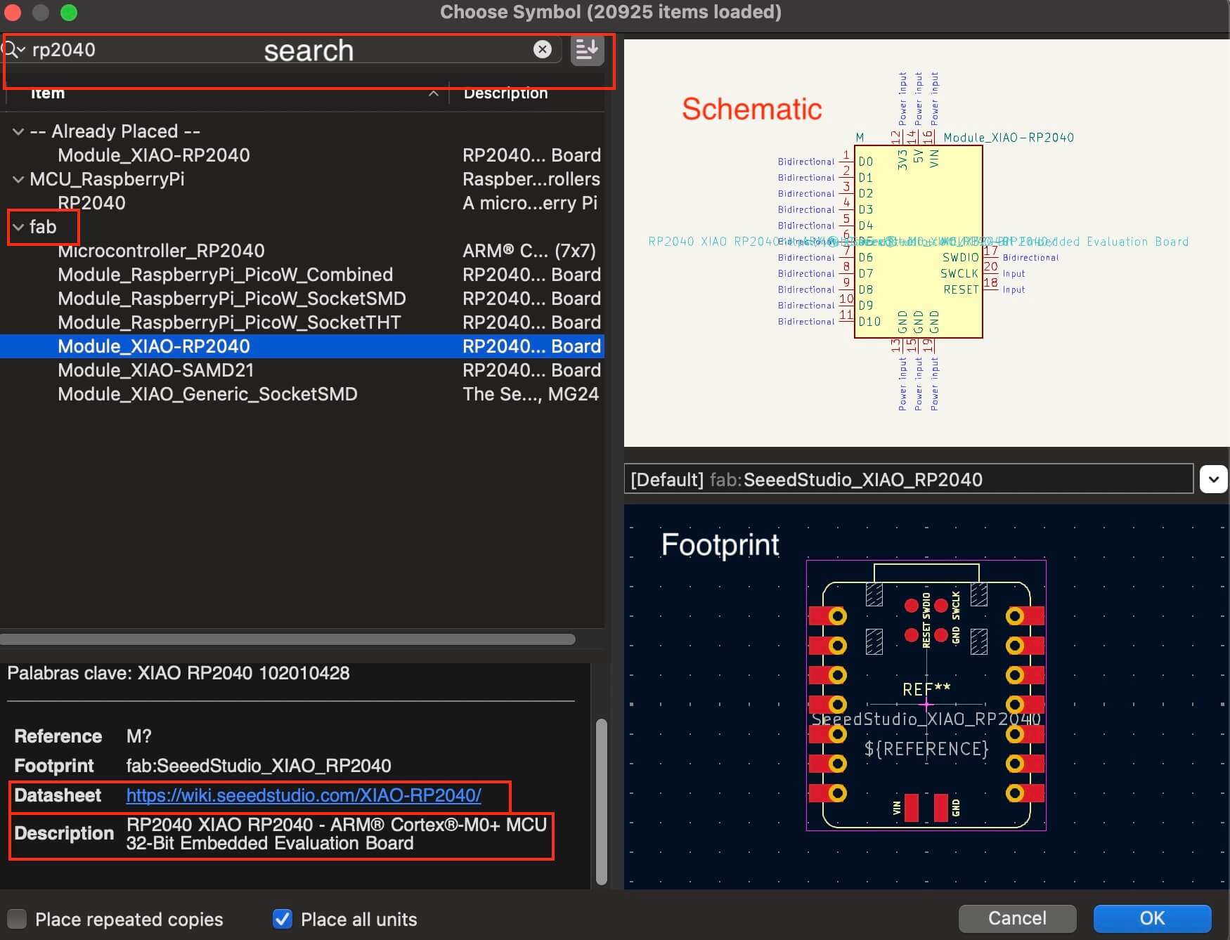
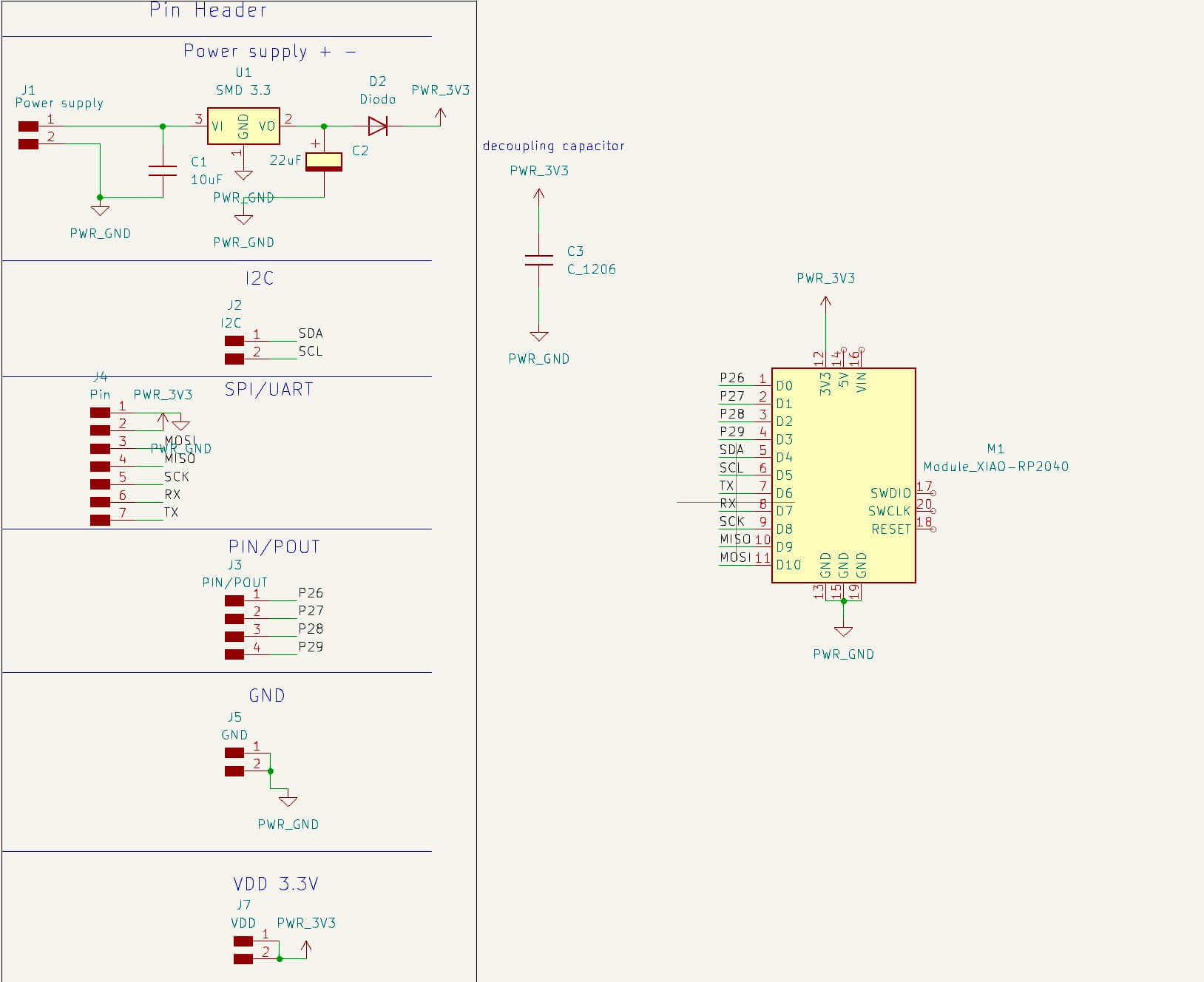
Once we are in the "Schematic Editor", it is necessary to select "Add symbols", since all the electronic components that we have will be found there. Selecting the option opens a new window, in which we can search for a specific component in the "search engine", ensuring that this component is found in the "fab" folder. When selecting our component, it should show us a view of the "schematic" and the "Footprint". In some cases, the components have a "Datasheet", in those cases it is recommended to see its information and know the different parameters that make up the component. If everything is correct, press "OK".
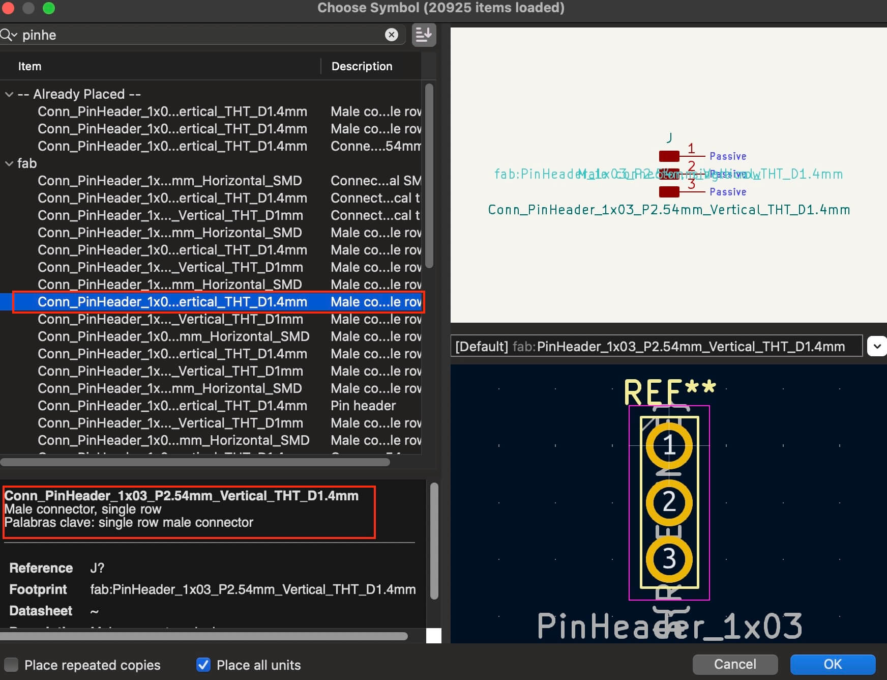
Once we press "OK", the component schematic can be placed anywhere in the work area. The next thing would be to place terminals to communicate with the outside, which can be used as analog/digital inputs and outputs or as communication ports ( I2C , UART and SPI ). To place the terminals, it is important to press "Add symbol (A)" again and in the search engine write "Pin header" where we can select the desired connector, in our case we will use the THT (Through-Hole Technology) types.
We place all the pins and order them, with the "Add label" option, we place labels to create the link according to the nomenclature and avoid wiring as well as to make a more organized design, we order and the schematic is as follows.
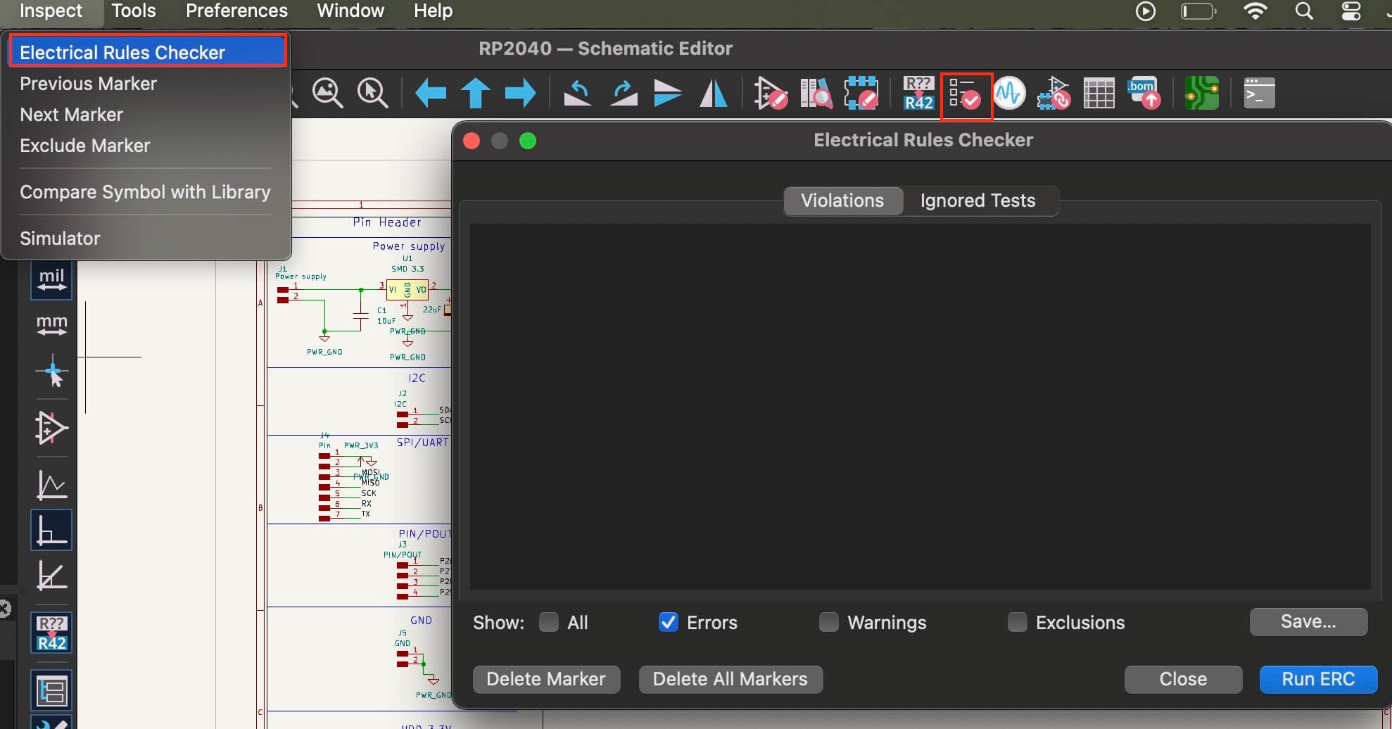
Once all the connections have been completed, the next step is to perform the "Electrical Rules Checker" or simply "ERC", the ERC consists of verifying the rules that must be followed to ensure that the electrical connections are made correctly under certain specifications. These rules are normally applied in the design of integrated circuits (ICs) and printed circuit boards (PCBs). In the following link some errors detected thanks to the "ERC" are presented.
To open the "ERC" we can press the icon shown in the image below or follow the path "Inspect - Electrical Rules Checker". This opens a new window and to start the review we must press "RUN ERC"
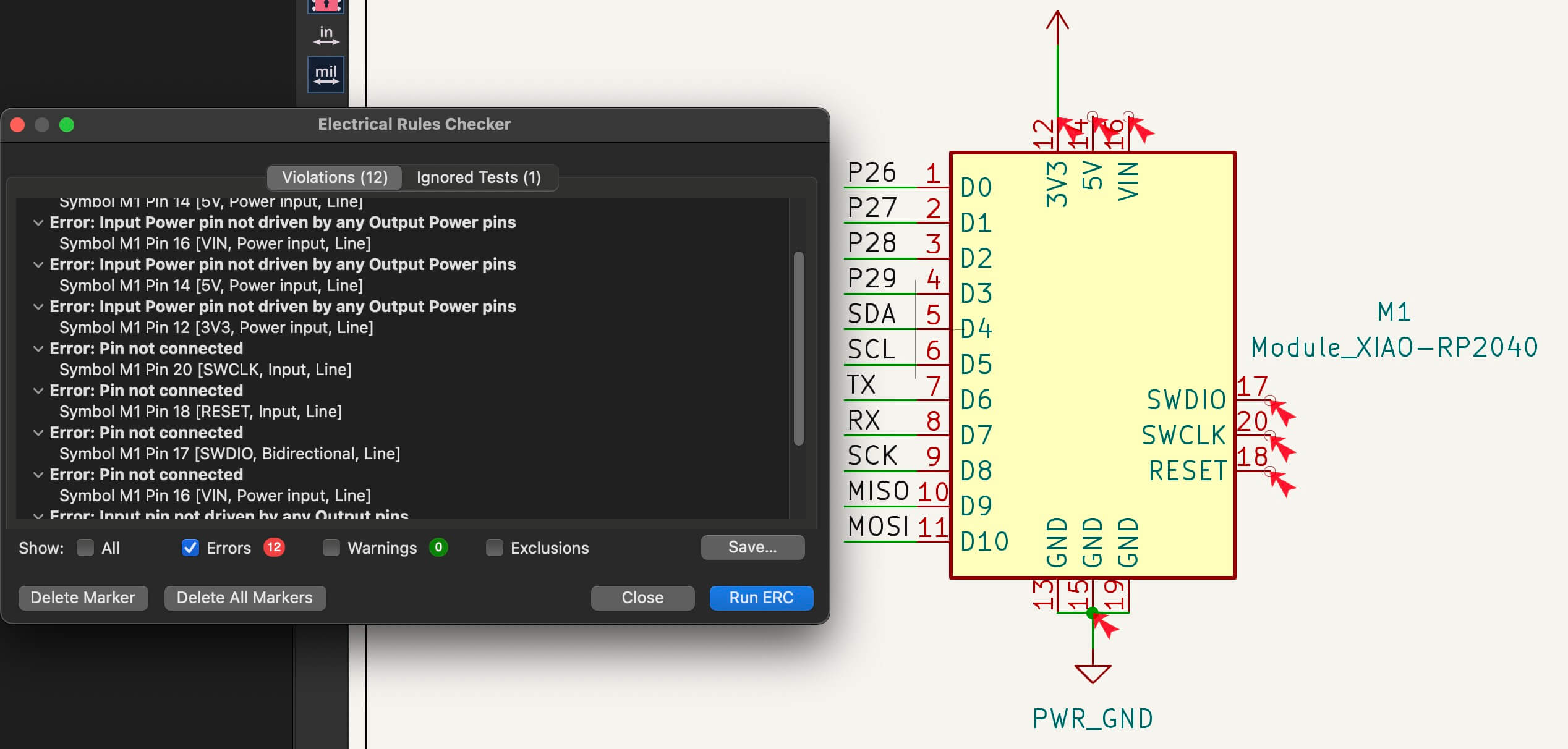
When running the "ERC", it will give us "Warnings" and "Errors", the warnings are alerts and the errors are violations of the design rules. As seen in the image below, there are 12 errors, which are related to the lack of connection of all the pins. Although they are errors, we are aware of why those pins are not connected, and in this case, we can ignore the errors.
If the editing of the schematic has finished, we can go to the "PCB editor", remembering that we can always return to the schematic to make changes.
PCB Editor
Once we are in the "PCB Editor", it is necessary to select "Update PCB from Schematic", which will open a new window where it shows us all the schematic elements that are going to be imported.
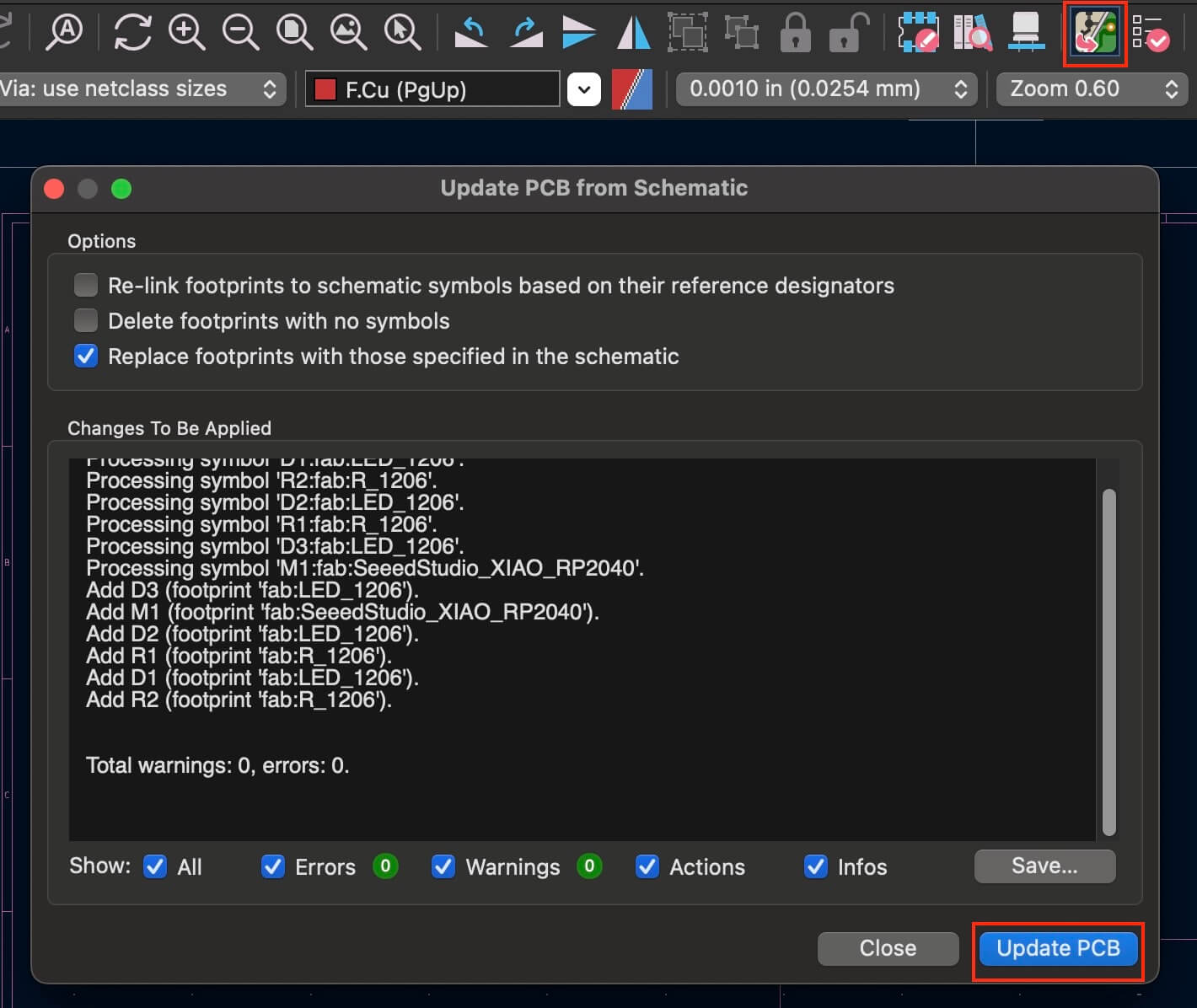
By pressing "OK" in the previous step, we place all the components but in an unordered way.
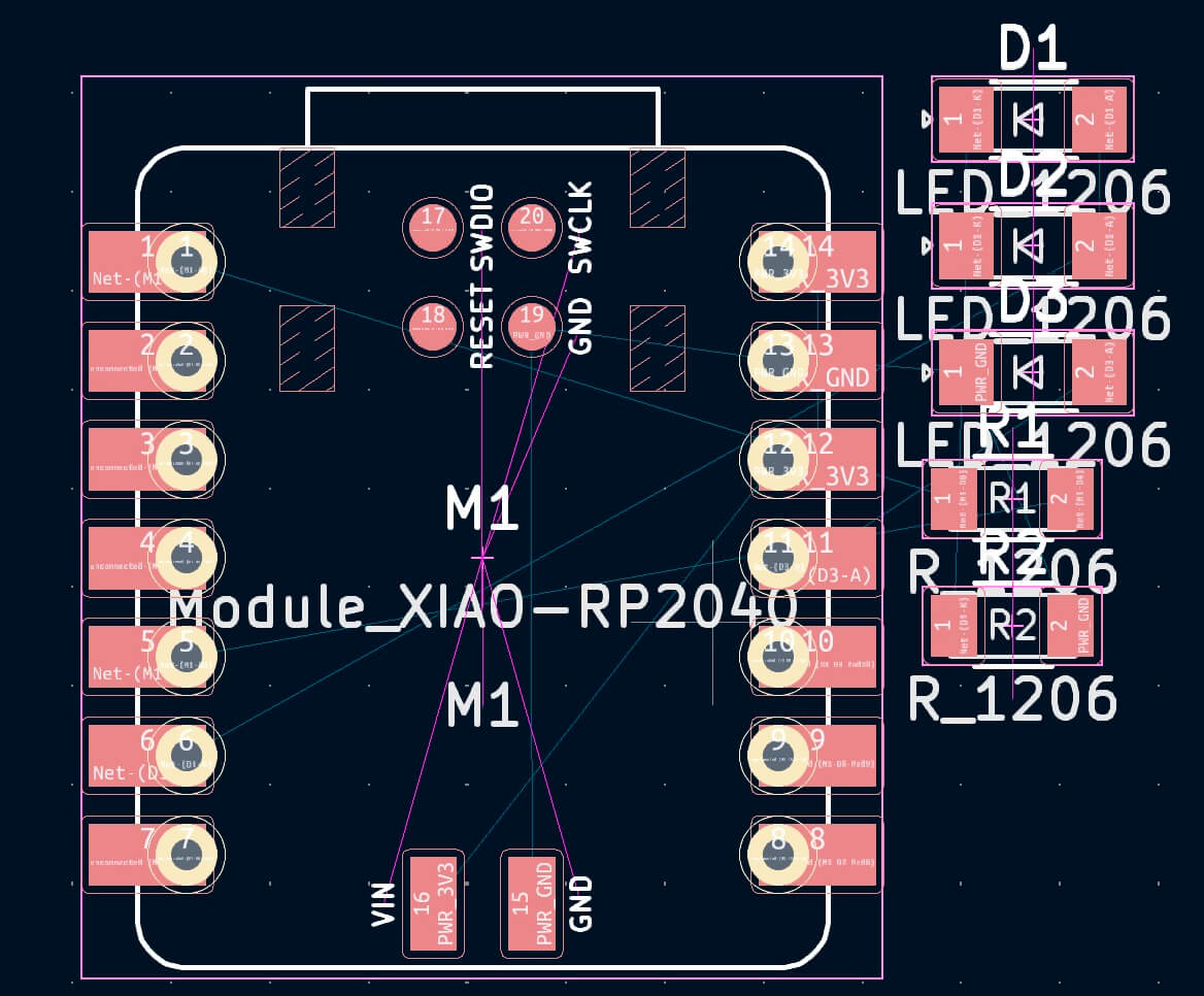
We must order all the components according to our requirements, as well as the position of the inputs and outputs of the board. Below is the distribution with which our board was designed.
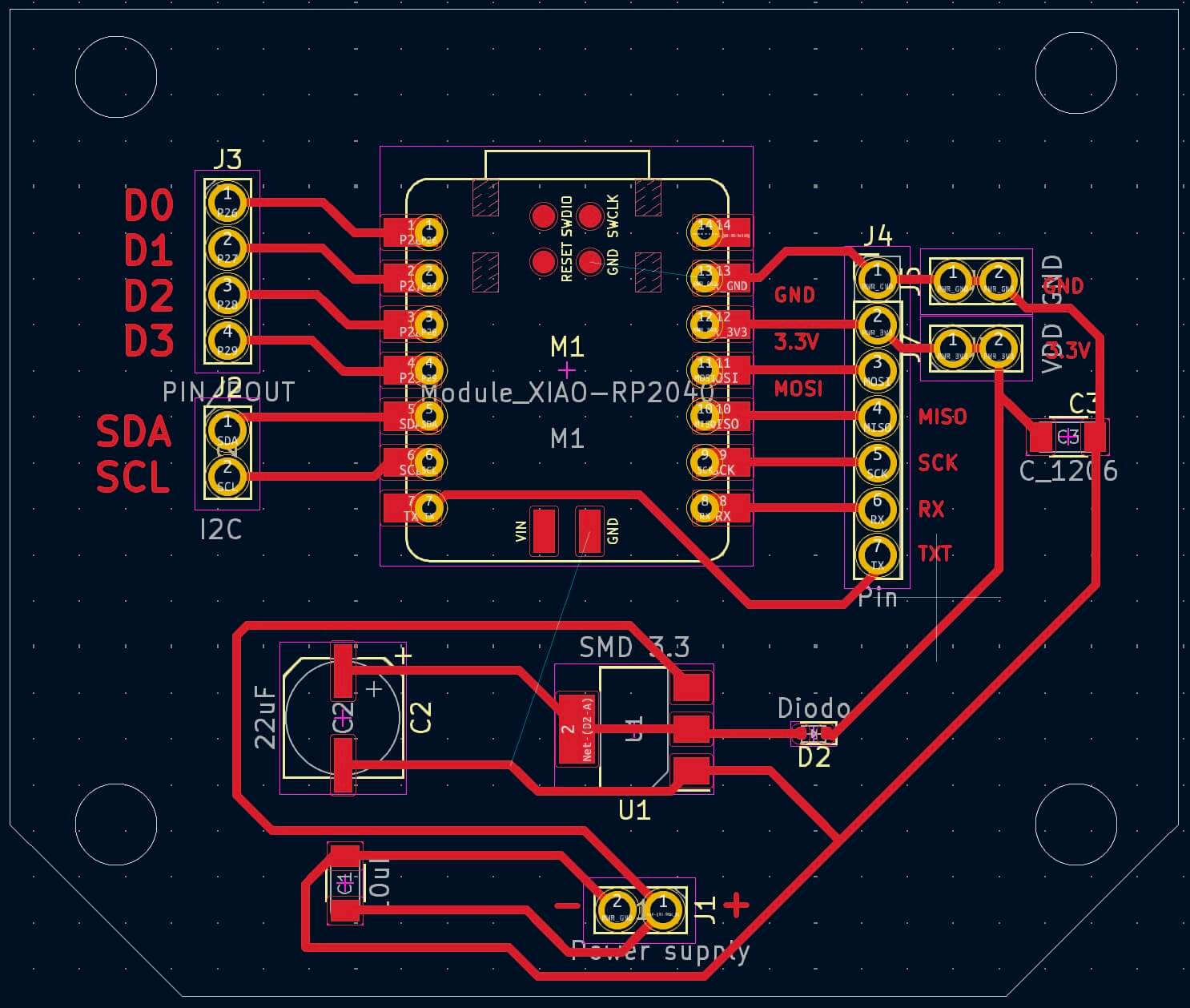
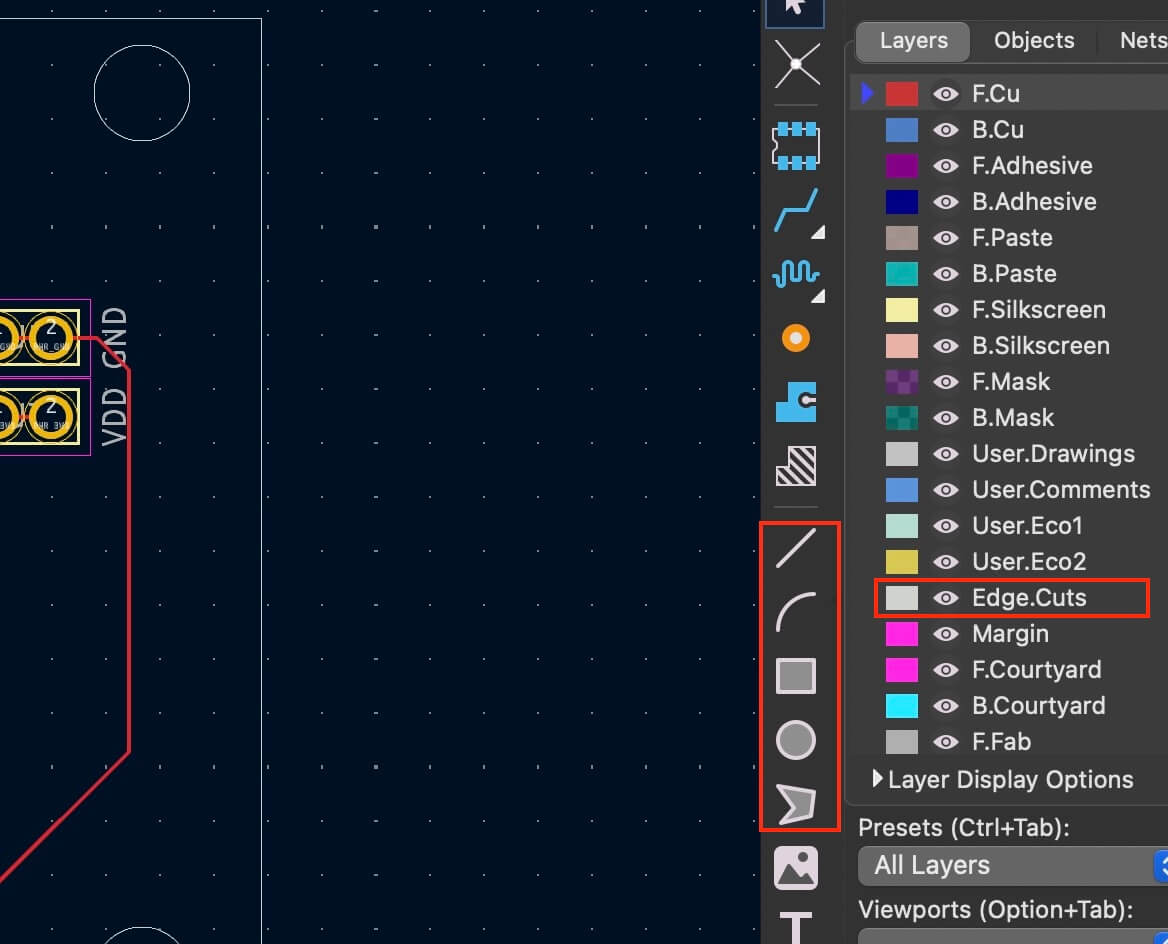
If the distribution of the components is correct, we can place a cutting edge, which is done by selecting "Edge.Cuts" and a type of stroke.
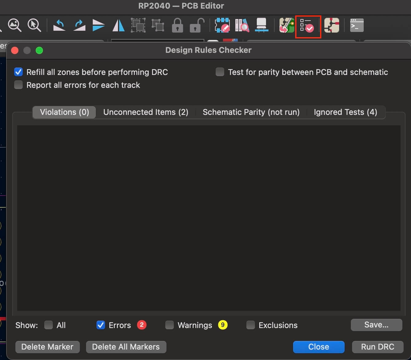
Before finishing, it is important to perform the "DRC", the following link shows basic and common types of DRC rules.
We press the "DRC" icon; This opens a new window, and we press "OK", when we do this, the design rules compare our design and show us all the violations and errors that exist, when we click on each error, it marks the place in the "Layout", where the error is located, so that the correction can be made. There are errors that we can omit under our consideration and based on knowledge of electronics.
To visualize what the PCB would look like, we go to the "View - 3D Viewer" menu.
PCB Calculator
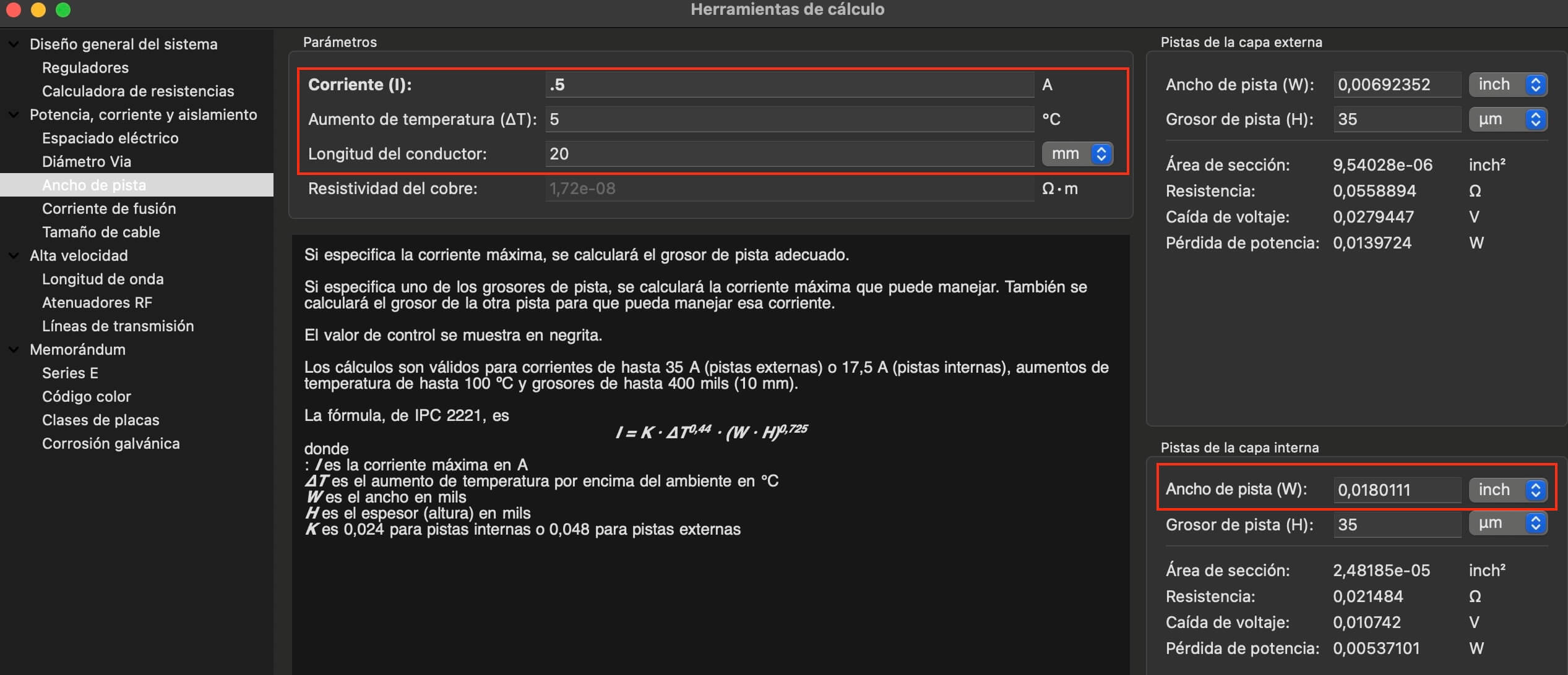
One of the most important tools of "KiCad" is "PCB Calculator", in it you can make all kinds of calculations regarding the "PCB". In order to access the calculator, it is necessary to press the "Calculator Tools" icon.
With the previous step, a new window opens in which we can choose the type of "calculation" we want to do. Among the elements that can be calculated, some are mentioned below.
- Track widths
- Fusion current
- Wire size
- Wavelength
- Transmission lines
- Color codes
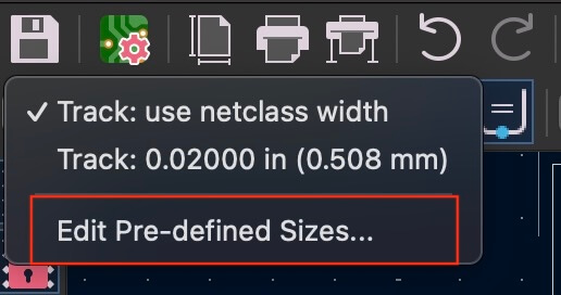
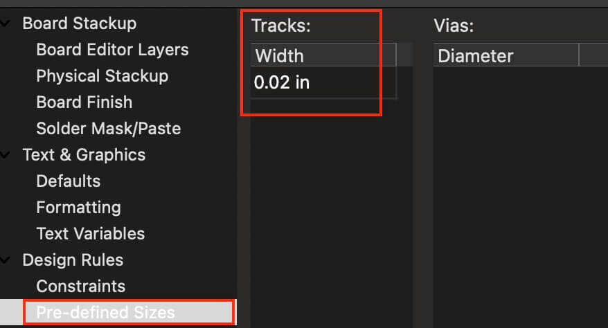
At the moment we are interested in knowing the track width, taking into account that the "XIAO RP2040" handles a maximum current of 500mA through its power pin, although the GPIO pins handle a maximum of 15mA, to maintain the same line width throughout the PCB it is decided to only do the calculation for a current of 500mA and a temperature increase of 5°C. Which results in an approximate width of "W=0.02 inch".
These new width data must be entered in the "PCB Editor" to perform the routing, the following images show the steps.
Design Rules
To access the design rules, press the icon indicated in the figure below, by doing so opens a window with all the configurations that can be made on the board. We head to " Design Rules", where we are going to focus on the most important elements in our design, such as:
- Minimum clearance
- Minimum track width
- Minimum through hole
- Hole to hole clearance
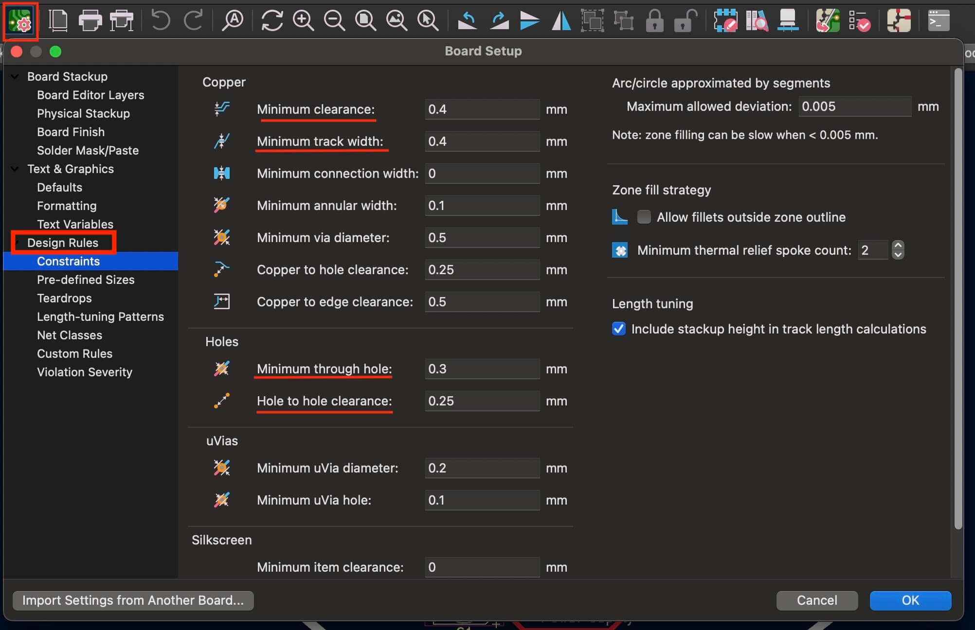
It is important to note that these values can be changed depending on our needs or specifications, in our case we will leave them with the default values.
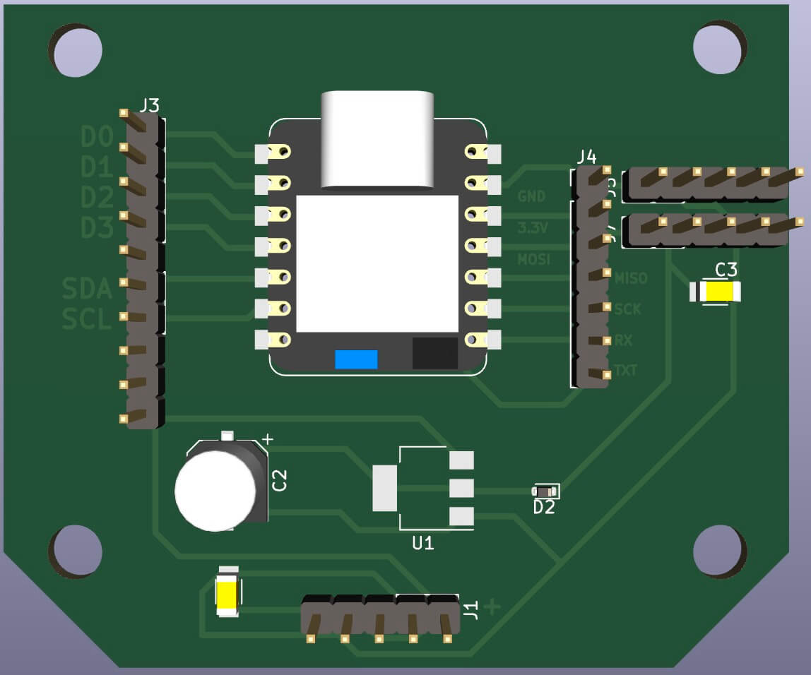
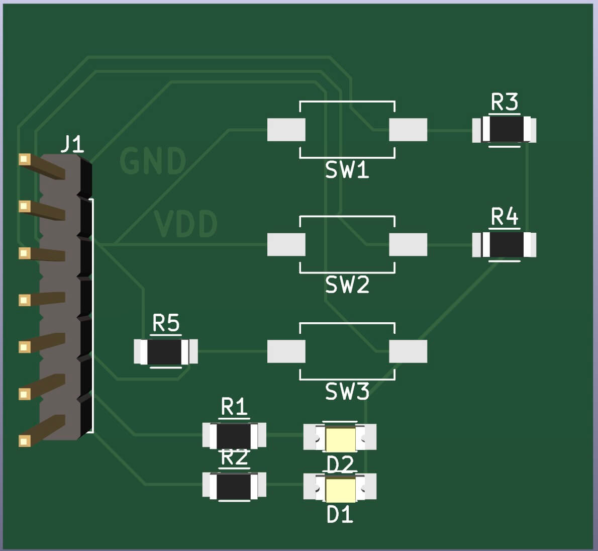
TEST PCB
As the main board only consists of inputs and outputs, it is necessary to design a test board to test the correct routing of the PCB. The following images show the schematic, as well as the "PCB" and the "3D" image.
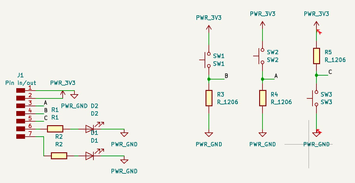
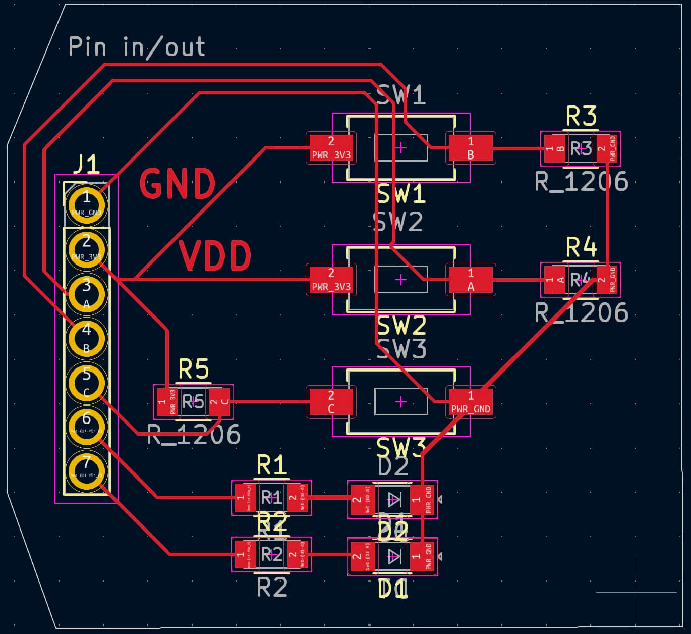
Let's note that the outputs of the test board have LEDs, which for protection must have a resistor. According to the “data sheets”,
the maximum voltage supported by the LED is \(3V\) and the nominal voltage is \(2.85V\) with a current of \(60mA\). If the output of the xiao RP2040
is \(3.3\) volts, it is necessary to calculate a protection resistor.
Applying Kirchoff's voltage and Ohm's laws, the following results are obtained:
\(R_{max}=\frac{V}{I}=\frac{V_R}{60 mA}=7.5\Omega\)
\(V_R=V_{CC} - V_{Dmax}= 3.3v - 3V=0.3\)
\(R_{min}=\frac{V_R}{60 mA}=5\Omega\)
So, there can be place a resistor between \(5\Omega\) and \(7.5\) \(\Omega\).
Design explanation
As you can see in the image, this consists of a regulator and two capacitors. The objective of placing the regulator is so that the XIAO RP2040 can be powered externally if desired, the 10 and 22uF capacitors are placed to filter the signals, and that the output is as clean as possible. It should be noted that this design was based on the manufacturer's datasheets, and that the capacitor values are based on the same datasheet, as shown in the image.
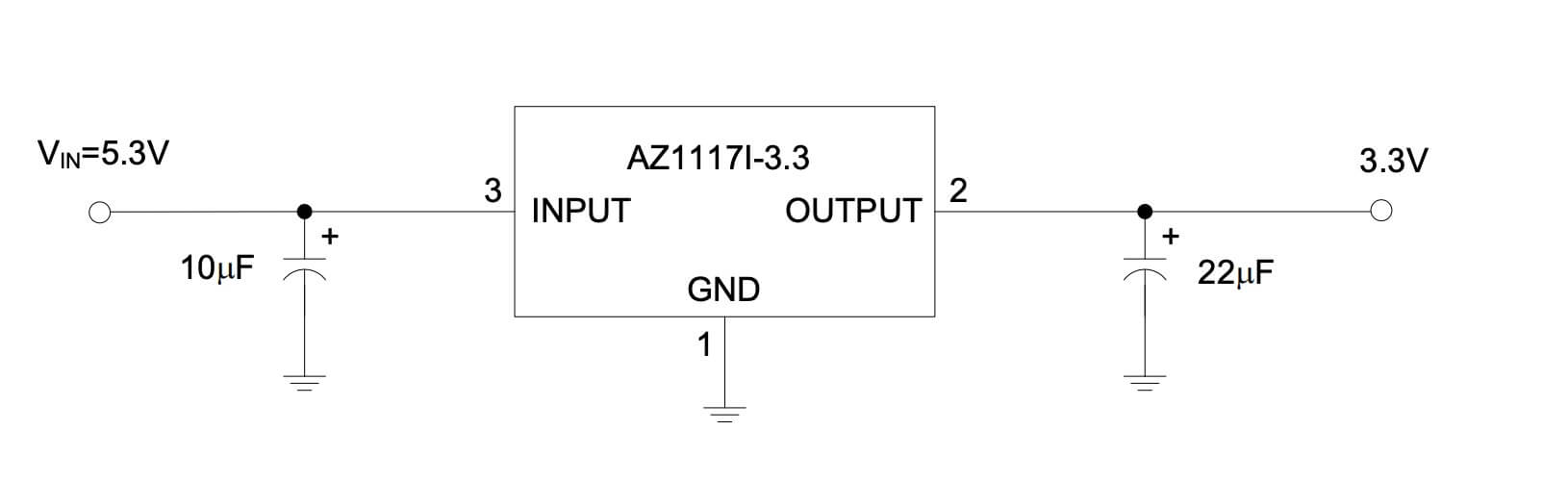
It's important to note that a diode was added to the regulator's output to prevent reverse current. While the provisionally proposed diode is silicon, it will most likely be replaced with a Schottky diode, as it only has a 0.3V voltage drop, leaving an output voltage of 3V, which is within the operating range of the XIAO RP2040.
Finally, a ceramic decoupling capacitor was tentatively placed to provide a local and constant source of power to the circuit, seeking to mitigate sudden changes in the power supply voltage. It can be noted in the layout that the decoupling capacitor is located very close to the XIAO's power input to prevent noise.
Learning outcome
This week we learned about electronic design automation (EDA), which is a tool that allowed us to design circuits with the objective of manufacturing PCBs following a series of steps and design rules (DRC and ERC). On the other hand, it is important to consider certain criteria when designing the diagrams, such as including capacitors between the power supply (recommended capacitor values from \(0.1μF\) to \(10μF\)) and GND with the objective of decoupling the signals, stabilizing the circuit voltages (avoiding fluctuations) and handling surge currents.