Electronic Design
Electronic design involves creating circuits and PCBs to achieve specific functions, considering factors like component selection, power requirements, and signal integrity. It requires a mix of theoretical knowledge and practical skills, from schematic design to PCB layout and manufacturing. Regarding the technical and theoretical aspects of circuits, I consider that my academic background has provided me with a solid understanding in this area. Nevertheless, the group assignment emphasizes the application of various tools that can assist not only in the manufacturing process of a PCB but also in the detection of issues such as damaged components, faulty pins, or signal inconsistencies.
This week, I will design a PCB for an ESP32 WROOM and give some general ideas for designing another board for a different microcontroller. There are multiple software options for PCB design, such as EasyEDA, Altium, Fusion360, Eagle, etc. However, since it is free and easy to use, I will use KiCad for my PCB design. Still, I will detail later why I will use KiCad to design practically all the PCBs during the FabAcademy.
Now, I could start explaining how the software works and introduce tools and board functionalities along the way. However, that would only result in a "recipe" for creating a specific PCB for the ESP32, not for other microcontrollers like the Attiny45, which even has a different architecture (as seen in the embedded programming group assignment). Therefore, I will first provide some general considerations to think about before opening any design software.
General considerations
- Setting a goal for the PCB: It may sound basic, but before even choosing a microcontroller, you need to define the board's limits and objectives. This simplifies the design and construction process.
- Check datasheets for key components: Review operating ranges like voltage, current, temperature, or frequency to ensure compatibility. This is crucial when working with complex circuits.
- Look for similar PCB examples: This is especially useful when working with microcontrollers. While the datasheet suggests components, looking at pre-made boards, like the Espressif Devkit for ESP32, helps form a clearer idea of what components are needed. From there, you can rely on your electronics knowledge to decide what is unnecessary.
- Choose a design software: Once the basic ideas are set, select the software for designing the PCB.
- Create the schematic diagram: In the chosen software, draw the circuit connections for the board.
- Design the PCB layout: Using the schematic, place the components and create connections on the PCB. Most PCB design software allows easy import of schematic components.
- Extras: Simulate, Validate, and Manufacture: The previous steps cover the PCB design process. From here, you can simulate the circuit in software or on a physical protoboard (with caution). Then, validate that the PCB meets its intended objectives. Finally, manufacture the board, whether by fabricating it yourself or outsourcing production.
For this week, I plan to design a PCB for the ESP32 WROOM. Below is a comparative analysis of various EDA software platforms, developed to identify the most suitable option for the specific requirements of the project to be implemented.
Feature Comparison Table
| Criterion | KiCad | Altium Designer | Eagle | EasyEDA |
|---|---|---|---|---|
| License and Cost | Free, open-source, no limitations for commercial use. | Proprietary, subscription-based, high cost. | Free tier available, but limited. Paid versions via Autodesk subscription. | Free with limitations. Primarily tied to JLCPCB services. |
| Platform Compatibility | Cross-platform: Windows, macOS, Linux. | Windows-only (native). Workarounds required for other OS. | Windows and macOS. | Web-based (no installation needed). Desktop version available. |
| Schematic & PCB Integration | Robust dual-environment with forward-annotation and DRC. | Highly integrated, with advanced design rule sets and constraint management. | Integrated, but less scalable for multi-layer boards. | Integrated interface, but limited rule customization. |
| Layer Support | Supports complex multi-layer boards with internal planes. | Optimized for high-density multi-layer boards (e.g., HDI). | Limited to 2 layers in free version; paid tiers offer more. | Up to 6 layers; optimized for JLCPCB processes. |
| 3D Visualization | Integrated 3D viewer with STEP model export and custom footprints. | Advanced 3D engine with MCAD integration (SolidWorks, Fusion 360). | Basic 3D view with limited export options. | Basic 3D preview for assembly, not customizable. |
| SPICE Simulation | Includes NGSpice integration for circuit simulation. | Integrated simulation environment with signal integrity tools. | External simulators required. Not natively included. | Only basic simulation via built-in tools. |
| File Ownership | Full ownership. All files are stored locally and open-format. | Local files, proprietary formats. | Cloud-dependent licensing, partial file control. | Cloud-centric; data tightly coupled with JLCPCB ecosystem. |
| Plugin & Scripting Support | Supports Python scripting and a wide array of community plugins. | Proprietary scripting environment, limited community-driven plugins. | Minimal scripting support. | No scripting functionality. Closed environment. |
Based on the comparison, I chose KiCad as the platform best suited to meet the project and future assignments. This because it allows you to start working immediately without worrying about licensing or access restrictions, which makes it ideal when working on multiple prototypes or personal projects. Since it's available on any major operating system, it is very easy to switch between computers without dealing with compatibility issues. The files it generates are completely under your control, with no dependencies on online services or locked platforms, which is convenient for managing backups or working offline. Although its interface may seem more complex at first, it provides all the tools needed for multi-layer routing, footprint editing, and even 3D visualization. It also offers automation through scripting, which can save a lot of time if you are repeating similar tasks. Overall, it is a very capable tool that gives you freedom and control without limiting how far you can go with a design.
Initially, I considered making a simple board for the microcontroller, but as I refined the design, I realized it closely resembled an Espressif Devkit, with differences in size, layout, and selected components. I included only the necessary features, such as GPIO connections and I2C/UART communication, basing much of my schematic on Espressif's design.
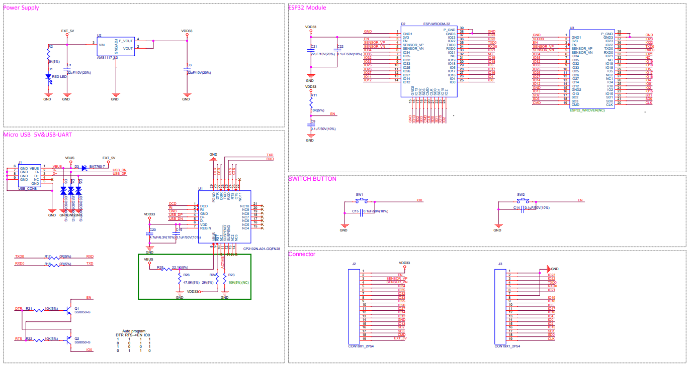
Figure 1: ESP32 WROOM PCB Espressif Design.
Additionally, while I intend to design a dedicated PCB for my final project, this board should also function as a backup for testing. This means the ESP32 needs a reliable voltage regulator to prevent damage from the battery voltage. To address this, I will use two voltage regulators: one for converting USB input (5V to 3.3V) and another for stepping down an external voltage (Vin to 5V). The output of this second regulator can then be connected to the first one to ensure a stable 3.3V supply for the microcontroller.
To build the PCB, it's essential to understand how each component functions within the schematic. I mention this because each component must have a corresponding footprint in the PCB design software to ensure proper placement and connectivity during fabrication. Without the correct footprints, the physical board won't match the schematic or, if there is no footprint attached to the component, the PCB will simply not be fabricated.
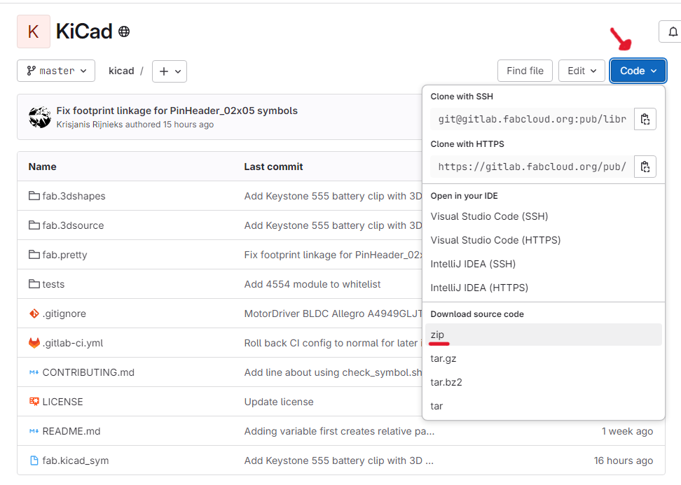
By default, KiCad includes some components with their respective footprints. However, for more complex circuits, this is not always the case. Our instructor, Oliver, provided us with a link to the Fab repository, which contains the necessary files to import additional components into KiCad. These components are also available in the lab, making PCB fabrication easier.
Here is the repository link and the step-by-step process to load new components and footprints into KiCad.
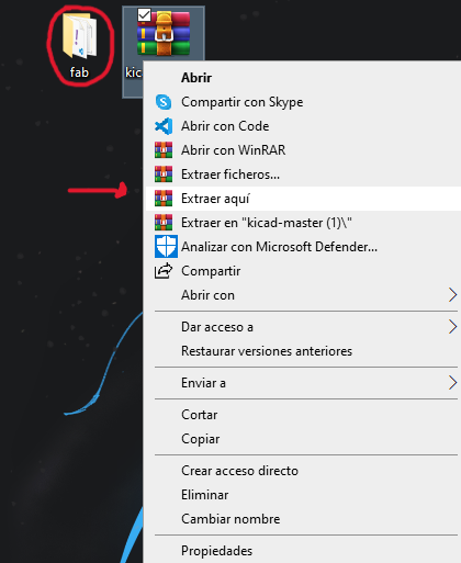
Download the libraries and decompress the files
Configure Symbol Library
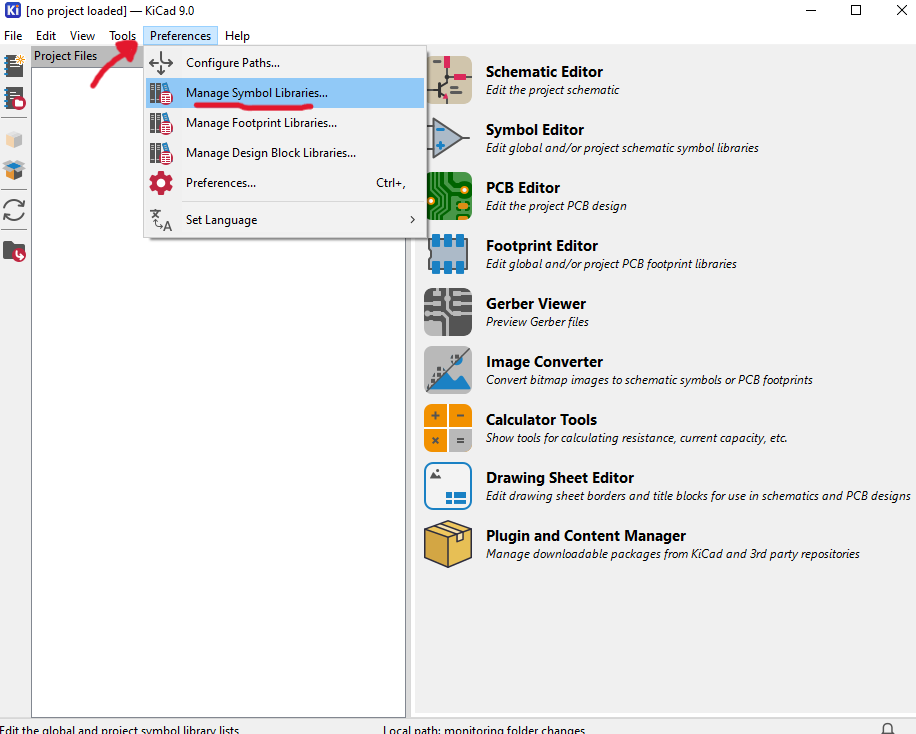
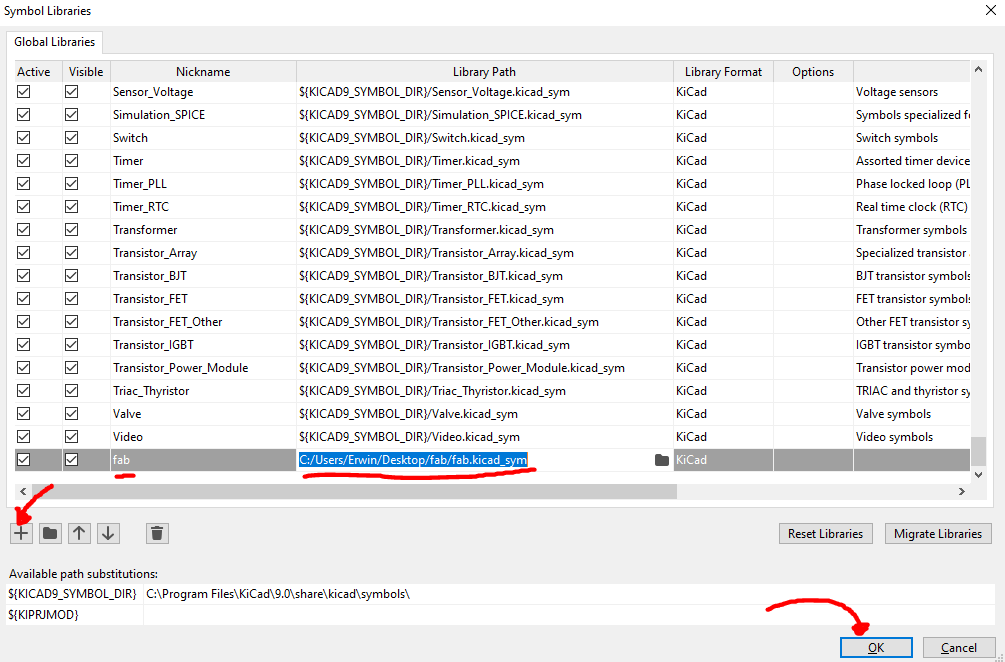
- Create an empty row: Add a new empty entry for the library.
- Name it with fab (in this case): Assign the name "fab" for consistency.
- Link the path to the “fab.kicad_sym”: Set the path to the correct symbol library file.
Configure Footprint Library
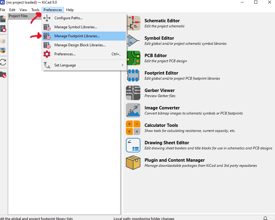
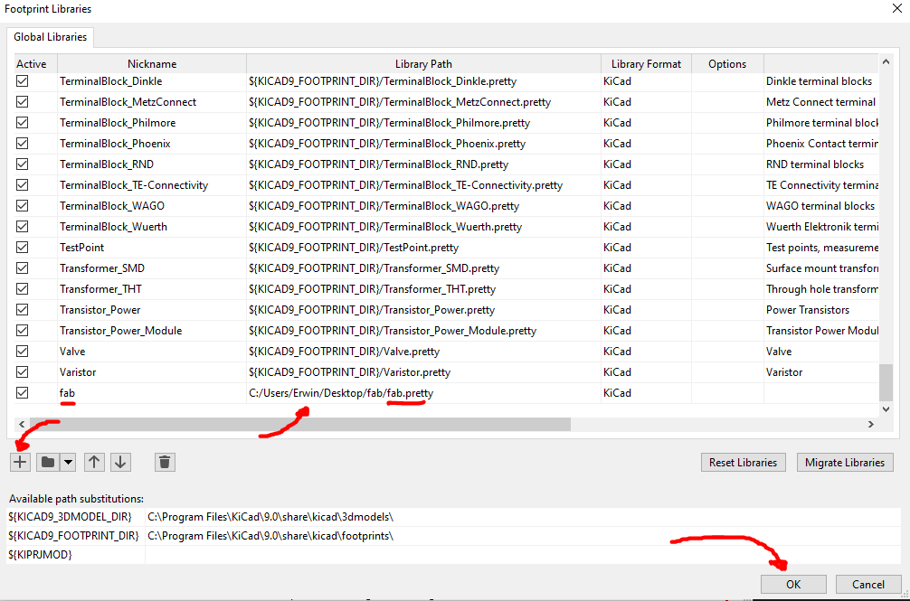
- Create an empty row: Add a new empty entry for the footprint library.
- Name it with fab (in this case): Assign the name "fab" for consistency.
- Link the path to “fab.pretty”: Set the path to the correct footprint library file.
Configure Paths
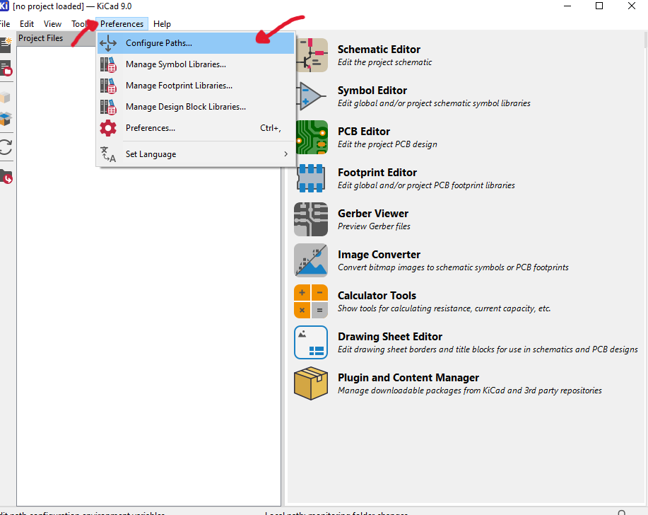
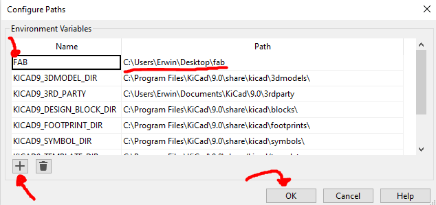
- Create an empty row: Add a new empty entry for the path.
- Name it FAB (in this case, notice it is in capital letters): Assign the name "FAB" in uppercase for distinction.
- Link it to the complete folder: Set the path to the main directory containing the libraries.
Once this is done, we can start our project. On the main menu, we can find various tools on the right to edit our project, including schematic editing, PCB layout design, and footprint management. Among these tools, there is one particularly useful for both the schematic diagram and PCB design. It allows calculations for component connections and helps determine the proper trace width. I will use this tool later for the trace width calculations.
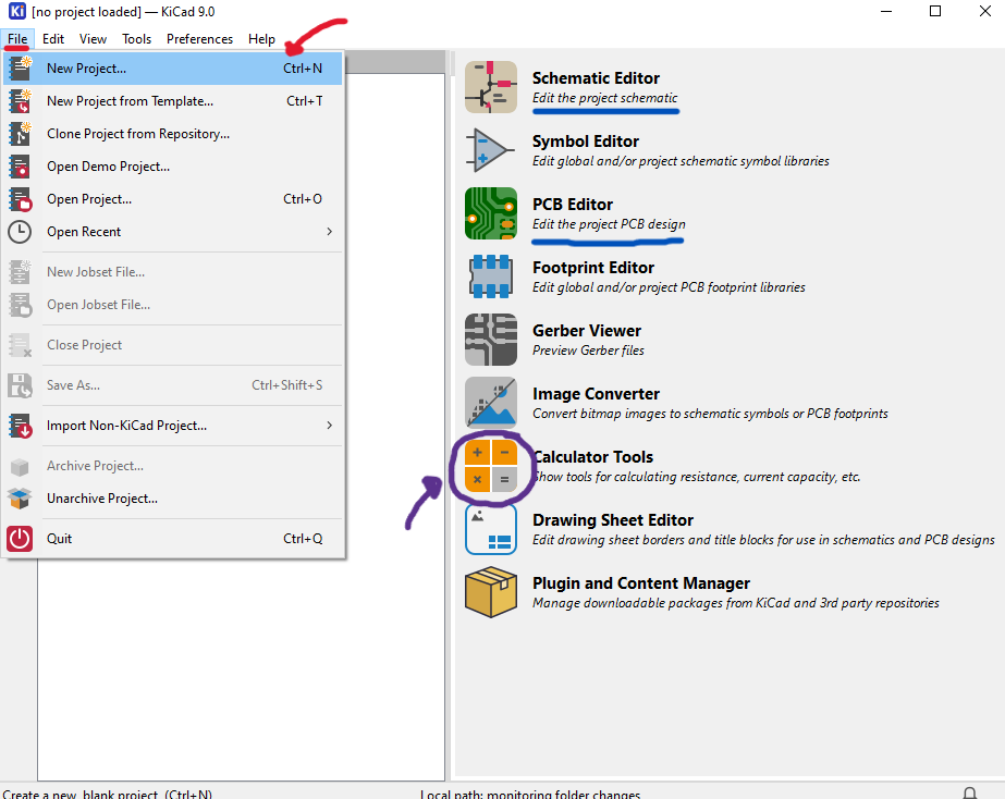
Figure 10: KiCad Main Menu.
To begin, we will start by editing the schematics. Here, we will create the connection diagram using the tools on the right to accomplish the following:
- Add Symbols (A): Here you can find and add components to the schematic (try to find fab library for footprint).
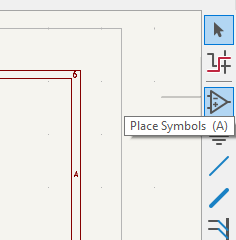
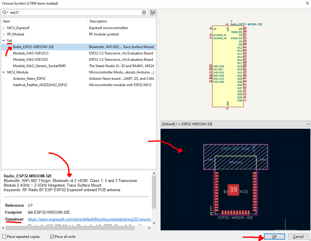
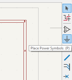
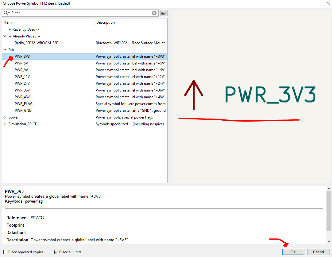
- Add Power Symbols (P): With this you can add power symbols that work like power labels (ground and different voltages).
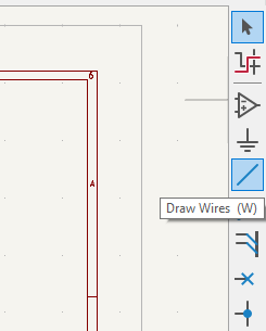
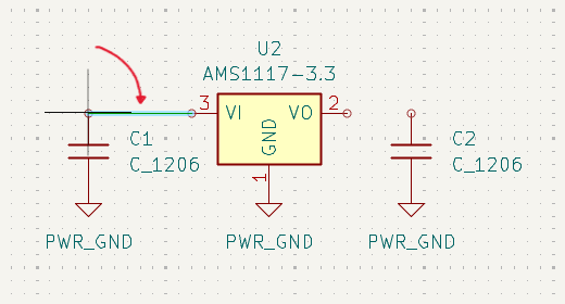
- Draw Wires (W): To connect components.
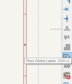
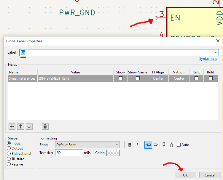
- Place Global Labels (Ctrl+L): To reduce wires and maintain a cleaner view, making a connection between two components without a visible wire.
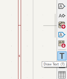
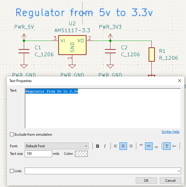
- Draw Text (T): If you want to add a note.
- No Connection Flags (Q): For pins that have no connection.
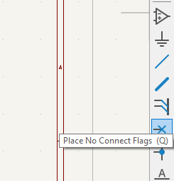
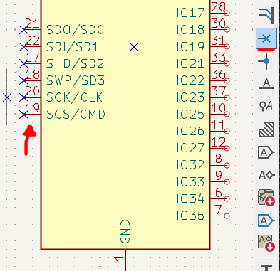
An important consideration for my board design is that the Espressif schematic includes a section on wiring a USB port and a USB-to-UART converter, which can be added for programming the ESP32. However, I will be using an external converter, so instead of integrating it into the board, I left the RX, TX, GND, and VCC pins accessible for easy connection. For the GPIOs, I just leave their pins accessible for easy connection. Finally, to test the board, I connected an LED to GPIO 15 and a button to GPIO 2. This way, once the board is manufactured, these components can be used to verify the board functionality.
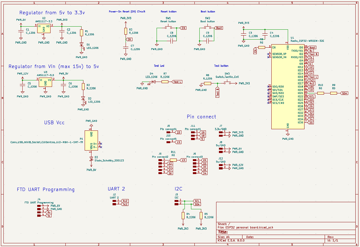
Figure 23: ESP32 custom board schematic.
One detail I want to highlight is that my original schematic was different. When it came time to lay out the PCB, I ran into several issues, so I made some changes. In some cases, I reduced the number of pins, rearranged them, and added 0-ohm resistors as bridges to make the connections easier.
To ensure everything is correct, KiCad provides a tool called "Electrical Rules Checker", which checks for electrical issues in the design. It helps identify possible mistakes, but it is not foolproof. We still need to analyze our connections carefully, as some warnings might simply indicate unused component pins, which is not necessarily an error if they were intentionally left unconnected.
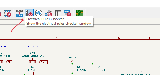
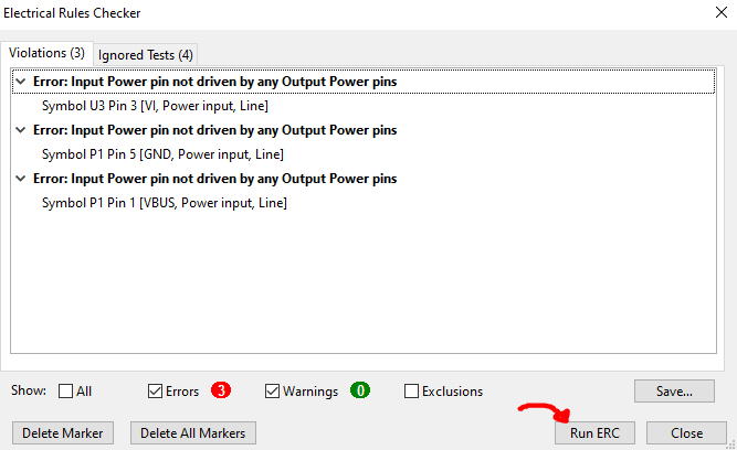
These errors reported by the Electrical Rules Checker are minor and will not affect PCB fabrication. They simply indicate that certain power input pins are not connected to components marked as power outputs, which KiCad expects for logical validation. However, as long as the connections are correct and properly labeled, they can be safely ignored. They are more related to schematic completeness than to actual electrical functionality on the board.
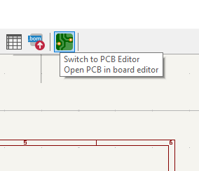
After fixing any errors or important warnings, we can move on to designing the PCB. To do this, we select the "Open PCB in board editor" option. Here, we will start working on the PCB layout by following these steps:
- Click "Update" at the top: To import schematic footprints.
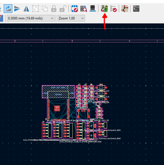
- Arrange the components: Position the components in a logical layout.
After fixing any errors or important warnings, we can move on to designing the PCB. To do this, we select the "Open PCB in board editor" option. Here, we will start working on the PCB layout by following these steps:
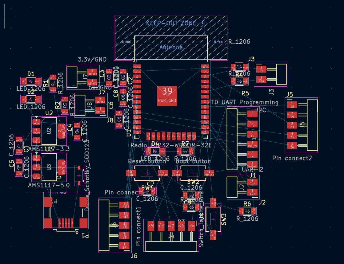
Figure 28: Arranging components in PCB editor (v1).
Another thing I want to highlight is that when placing the components, you can choose how to arrange them, but if you have limited PCB layers, it's best to plan their order based on the connections. In other words, focus on the hardest components to place and connect first, before the most important ones. I mention this because I did not consider it at first, and later I had to redesign the entire PCB.
In fact, while arranging the board, I was also making certain connections that I thought were a priority because of their complexity.
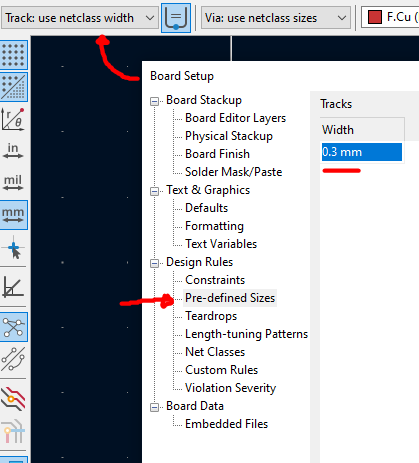
- Set the track width: Define the track width according to power requirements. I use the Calculator Tools mentioned earlier to determine the appropriate width.

- Route all the tracks: Connect all components using PCB traces.
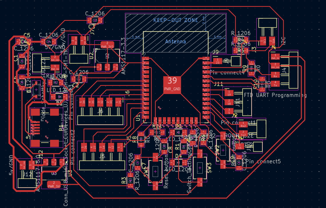
Figure 31: Laying out PCB tracks.
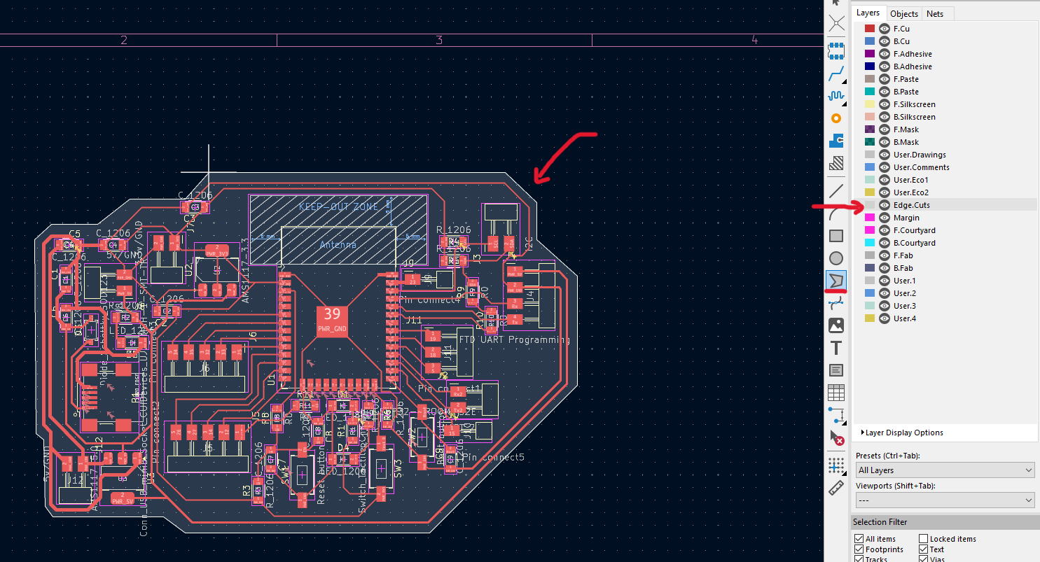
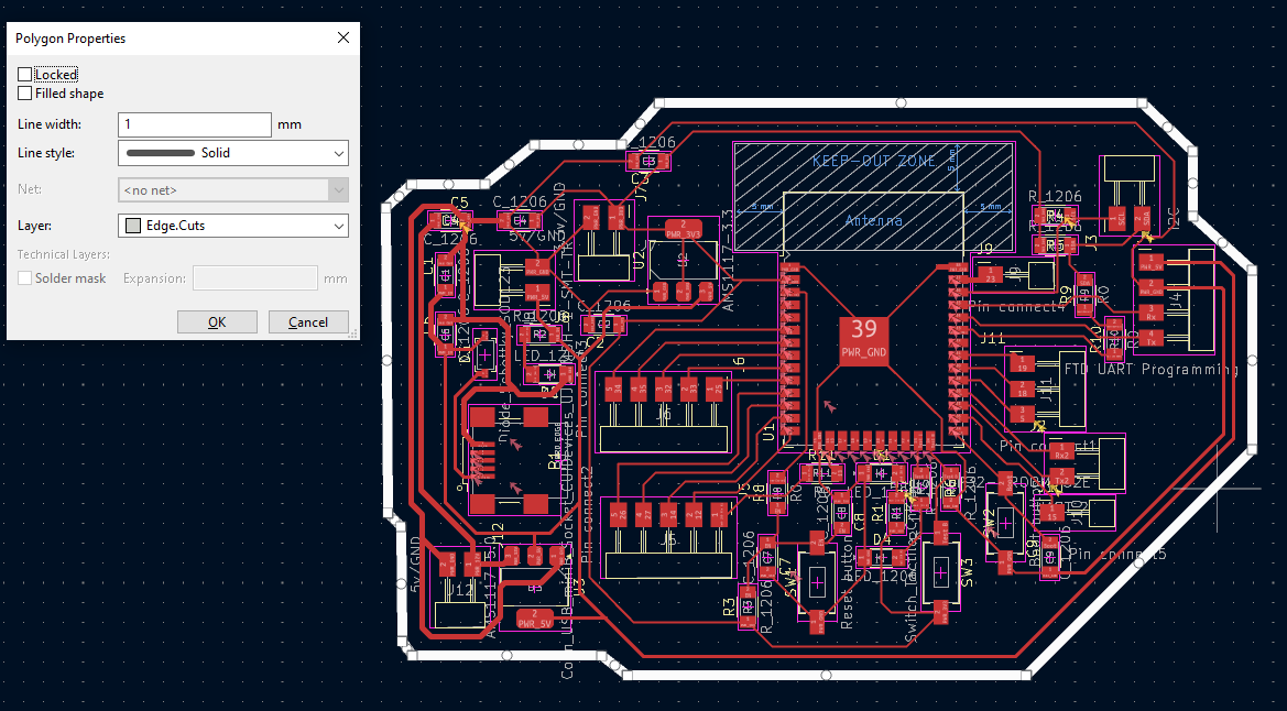
- Switch to the edge cuts: Create a 1mm border in any shape (this because of the diameter of the tool during the fabrication).
At first, I wanted to create a more visually appealing design. However, due to the complexity of the circuit, I did not distribute the components well enough to achieve a more interesting shape. I could go for a more extravagant design, but at this point, it would just be forcing the layout and wasting material. So, for now, this PCB will have a simpler shape.
Finally, just like the Electrical Rules Checker, KiCad has a Design Rules Checker for the PCB. It works similarly by identifying potential issues. Running this tool helps verify the design, and if any critical errors or warnings appear, adjustments should be made accordingly.
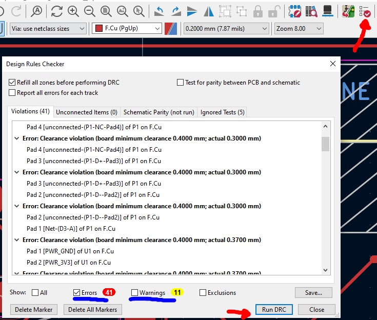
Figure 34: Running the Design Rules Checker in KiCad.
In this case, even though there are over 40 errors and 11 warnings, there is no reason to worry. Just like with the previous rules tool, it is important to review the marked errors carefully, as they aren't always critical. Here, for example, I get an error because I set a minimum spacing of 0.4 in the Board Setup, while some footprints have a spacing of 0.3-0.37. This is not a major issue, I set this parameter to help prevent soldering problems during manufacturing. So, as for the warnings, they are all related to the text. Since these will not affect the manufacturing process, they are completely negligible
After resolving the errors, the PCB design is complete. To get a better view, we can use the KiCad 3D Viewer. Here are the results…
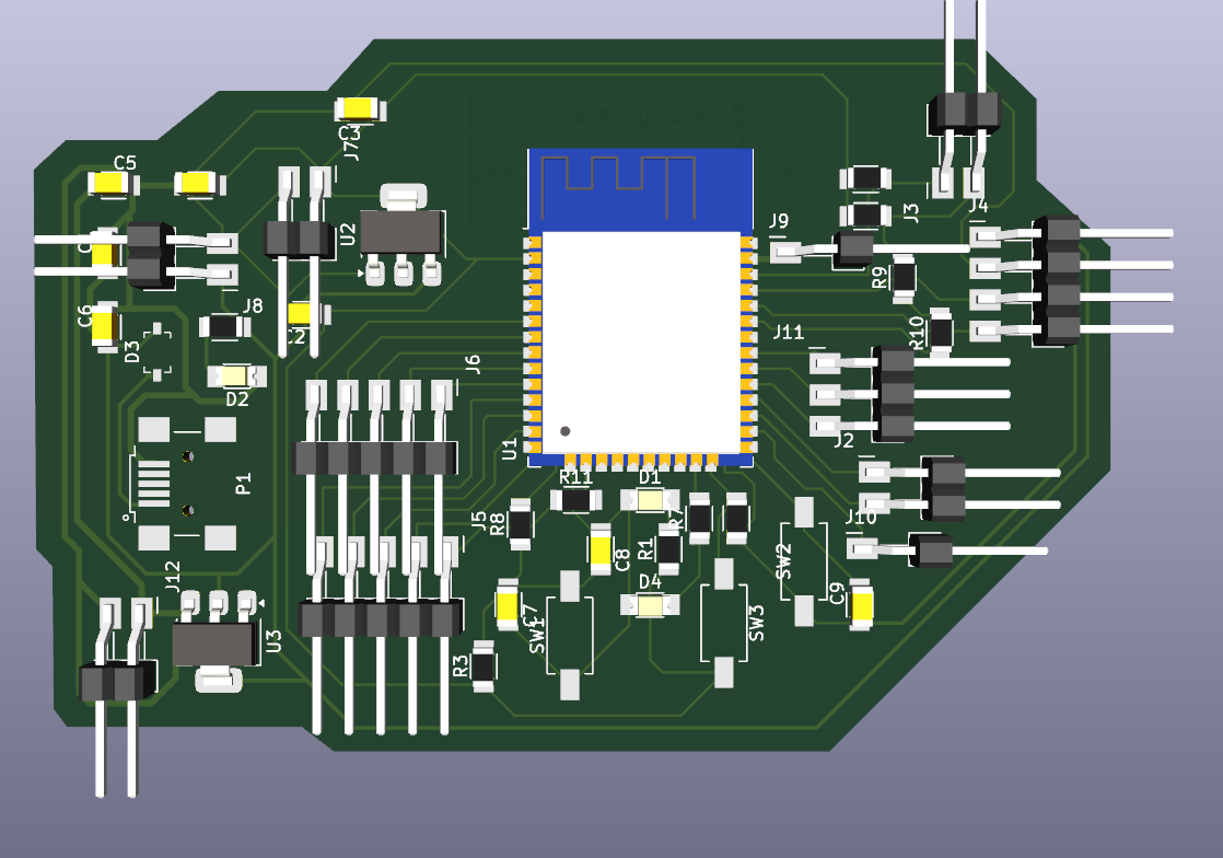
Figure 35: 3D view of the finalized PCB design.
The pins may look odd and could cause issues on the PCB, there is no nothing to worry about. Their orientation will be vertical once the PCB is made. I chose these superficial pins to avoid any manufacturing complications
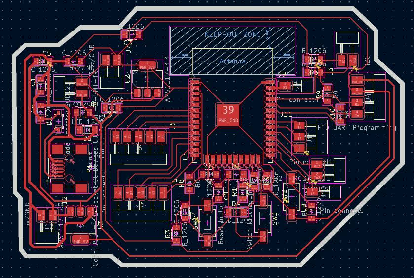
HEROSHOT! (The board looks better like this :3).
LEARNINGS
Without a doubt, the biggest lesson I learned here was not to underestimate PCB design. I already had some experience with KiCad, because a board I designed for the ATmega328P in a submarine project; and I have the necessary circuit design knowledge from my studies. However, I had never designed a board with surface-mount components, less for the ESP32. So, because of the pin distribution and component sizes, I had to make several adjustments on the fly.
Additionally, in previous projects, all my boards were manufactured in China, and I never made one myself. This added another layer of difficulty since I did not have a second layer for routing connections. This experience has truly shown me everything that goes into designing a PCB.
