Week 8 - Electronics production
In this week's group work, Antti instructed us on how to manufacture physical PCBs. I've previously made PCBs using the photoresist method and ordered others, but this was my first time making PCBs using the milling method.
PCB milling
For my individual work this week, I manufactured the PCB designed during week 6. Initially, I assumed through-hole coppering was possible so that I could use the bottom side of the board as a ground layer, but since it isn't possible, I had to modify my PCB layout in KiCad.
Since the bottom layer of the board was not easily available, some space had to be made for the ground wiring. I removed the option to use a 12 V power supply, as 5 V is likely sufficient to drive the servos and the fan. I also moved some wires closer together to create space for the ground wires on the top layer. For diagonal wires, the D shortcut ("Drag Track, Keep Slope") is convenient for this operation.
Below is the updated schematic with these changes applied:
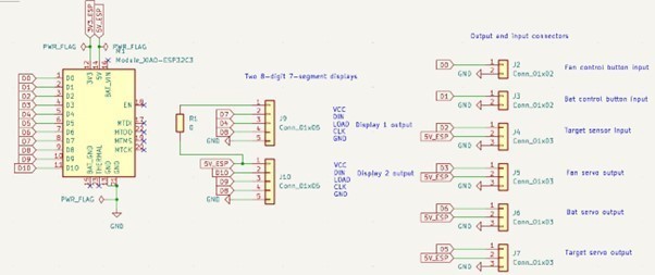
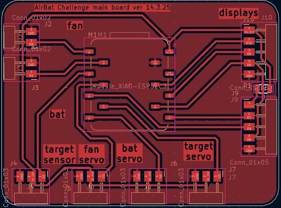
Here is the layout with everything placed on the top layer:
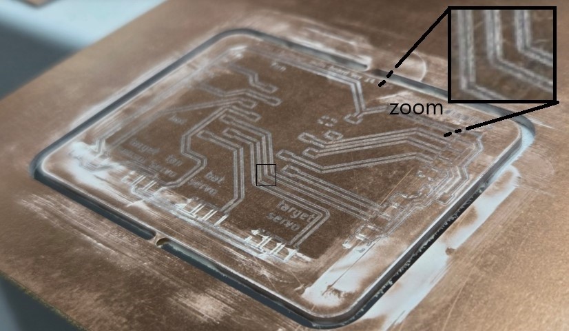
The board was manufactured in the same way as documented in the group work. However, the engravings did not fully cut through the isolation areas; only the edges of the isolated regions were milled with the 0.2 mm bit. Later, we realized that the LPKF CircuitPro software had a setting enabled that optimized the milling process by removing only the minimal amount of copper required for isolation gaps. With a solder mask coating, the board should still function correctly. I checked that there are no short circuits. Below is the board after milling, before cleaning:
Solder mask preparation
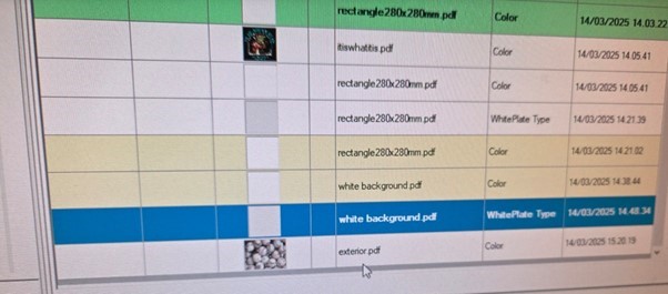
A solder mask and silkscreen were UV-printed on top of the PCB. The board was first cleaned with isopropyl alcohol to ensure good adhesion. To operate our Mimaki UJF-3042MkII UV printing machine, two PDF files are required: one containing the board outline (exterior.pdf) and another of exactly the same dimensions containing the solder mask and silkscreen design (interior.pdf). Areas of the PCB that should remain free of solder mask must be represented as solid white in the PDF file.
First, a printing position is selected using the Origin Setup function on the printer.
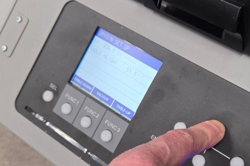
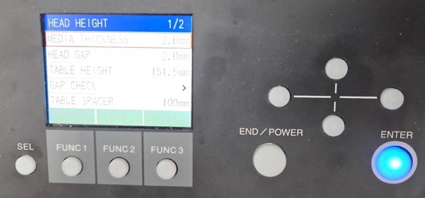
A media thickness of 2.6 mm was selected to match the thickness of the PCB.
The Mimaki RasterLink software was launched, and exterior.pdf, containing the board outline, was loaded first.
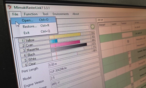
Exterior.pdf then appeared at the bottom of the list of printable items, where Print immediately was chosen.
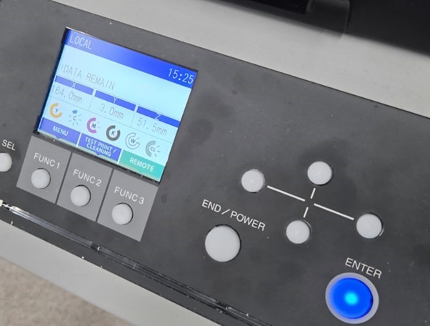
It then takes a few seconds until the printer display shows "Data remain", indicating that the file has been successfully sent to the printer. Then, press Remote. The board outline will be printed directly onto the printer table.
Next, the PCB is carefully aligned and fixed on top of the printed outline using double-sided tape. Then, the main graphic (interior.pdf) is printed onto the PCB in the same position, using the same process as before, except for color graphics it is advisable to use the "Special Plate" command with the options "Valid Pixel" and "Composite Automatically, Bottom" to create a white base layer beneath the main graphic, which improves the color quality of the final print.
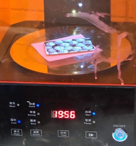
After printing, the UV-printed board can optionally be placed in a UV light tray for additional curing. This step is helpful for improving durability but is not strictly necessary.
Stuffing (PCB assembly)
The PCB only has a few surface-mount components, so I decided to solder these by hand. When attaching a component with many pins, I first melt a small amount of solder on one of the footprint pads and then place the component on top to hold it in position. After that, I solder the remaining pads by applying heat to the component leg for a few seconds, bringing in a small amount of solder, removing the solder wire, and then lifting the soldering iron once the solder has melted into a smooth, even joint:
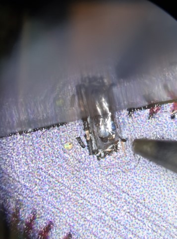
The pins for the ESP32-C3 need to be soldered horizontally so that they can slide easily on and off the headers. For this reason, the pins were soldered while being held inside a jig with straight headers. Additionally, the headers must be aligned properly on the board. To ensure this, the outer joints of the surface-mount headers were soldered first while the ESP32-C3 is physically connected. Then, the ESP32-C3 is carefully removed before soldering the remaining joints on the inner side of the headers.
Testing the microcontroller
Connecting to the microcontroller in the same way as described in the group work of week 6. Initially, I had trouble connecting because I chose the board “ESP32C3 Dev Module,” whereas in my case, I needed to choose “XIAO_ESP32C3. I tried a simple example program from the Arduino IDE called
DigitalReadSerial.ino.
		/*
		DigitalReadSerial
		Reads a digital input on pin 2, prints the result to the Serial Monitor
		This example code is in the public domain.
		https://www.arduino.cc/en/Tutorial/BuiltInExamples/DigitalReadSerial
		*/

		// digital pin 2 has a pushbutton attached to it. Give it a name:
		int pushButton = 2;

		// the setup routine runs once when you press reset:
		void setup() {
		// initialize serial communication at 9600 bits per second:
		Serial.begin(9600);
		// make the pushbutton's pin an input:
		pinMode(pushButton, INPUT);
		}

		// the loop routine runs over and over again forever:
		void loop() {
		// read the input pin:
		int buttonState = digitalRead(pushButton);
		// print out the state of the button:
		Serial.println(buttonState);
		delay(1);  // delay in between reads for stability
		}
This should print 0s in the Serial output when pin 2 is short-circuited to ground. However, this did not work: pin 2 remained in a zero state, except that it occasionally changed to 1 when I touched it with my finger. This was likely caused by static electricity or interference. I realized that I needed to enable the internal pull-up on pin 2 for this to work, so I did this by modifying one line:
One line changed to: pinMode(buttonPin, INPUT_PULLUP);
		/*
		DigitalReadSerial
		Reads a digital input on pin 2, prints the result to the Serial Monitor
		This example code is in the public domain.
		https://www.arduino.cc/en/Tutorial/BuiltInExamples/DigitalReadSerial
		*/

		// digital pin 2 has a pushbutton attached to it. Give it a name:
		const int buttonPin = 2; // GPIO2

		// the setup routine runs once when you press reset:
		void setup() {
		// initialize serial communication at 9600 bits per second:
		Serial.begin(9600);
		// make the pushbutton's pin an input:
		pinMode(buttonPin, INPUT_PULLUP); // Enable internal pull-up resistor
		}

		// the loop routine runs over and over again forever:
		void loop() {
		// read the input pin:
		int buttonState = digitalRead(pushButton);
		// print out the state of the button:
		Serial.println(buttonState);
		delay(1);  // delay in between reads for stability
		}
Now, the serial output correctly goes to 0 when pin 2 is short-circuited to ground:
Updates after week 8:
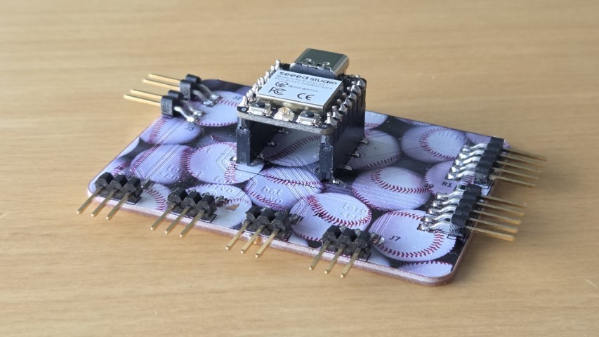
I designed and manufactured three PCBs overall:
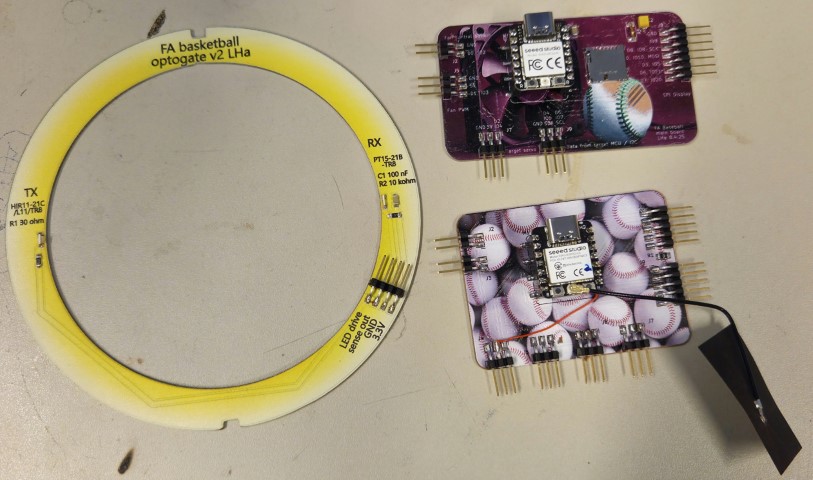
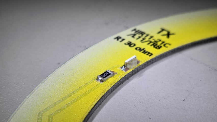
I placed the LED IR transmitter and phototransistor sideways pointing inwards towards the loop on opposite sides. (This was maybe Aleksi's idea?)
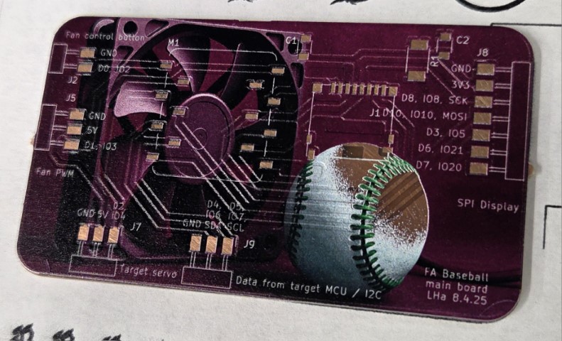
This was the new Board #1 for most of the game functionality, as described in week 11 documentation.
Design files
Board 1 Top copper layer Gerber file
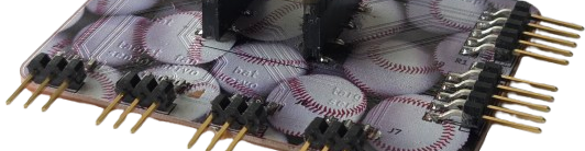
Board 1 UV printing main graphic (based on a ChatGPT prompt "Picture of a computer fan next to a baseball" combined with silkscreen from KiCAD)
Board 2 Top copper layer Gerber file
Board 2 UV printing main graphic (based on a ChatGPT prompt "Picture of baseballs to be used as a background" combined with silkscreen from KiCAD)
Optogate Top copper layer Gerber file
Optogate Edge cuts Gerber file