
Week 6 - Electronics design
This week's group work was to use the test equipment in our lab to observe the operation of a microcontroller circuit board. I hadn't used digital oscilloscope probes before, and I also got a refresher on how UART works.
For my individual work this week, I designed a PCB for my final project using KiCad, a free and powerful electronics layout software.
Fab Academy provides a component library specifically for the course, which I installed first by following these instructions
Design considerations
For my final project, I plan to use three number displays, two servos, two button inputs and one sensor.
Initially I have been planning to use SEEED STUDIO XIAO ESP32-C3 microcontroller. I'm concerned about whether it has enough I/O pins for all of the above external components. One way to achieve this is to use two 8-digit 7-segment displays with SPI communication (picture below) to display the three numbers and to share the CLK signal between the two displays. This way there seems to be just enough GPIOs available. Alternatively, a separate Arduino could be used to drive the displays. A speaker could also be a nice addition, but for now, I prefer to keep things simple.
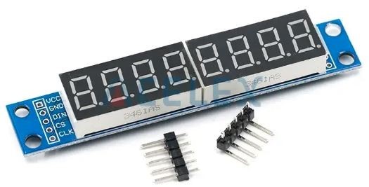
I may need 12V DC power to run the fan and servo motors. A convenient solution would be to use a PDC004-PD PD decoy module, which “tricks” a USB-C SMPS power supply into providing a fixed 12V output. I would then use a step-down converter to get 5V for the ESP32-C3. For now, I will simply add a 12V input on my PCB.
To keep my design flexible, I will use pin headers so that the microcontroller can be easily removed and replaced if needed. Fortunately, the XIAO ESP32-C3 already has a well-defined footprint in Fab Academy KiCad Library that can be used with pin headers.
PCB schematic entry
I placed the components and connected them with wires.
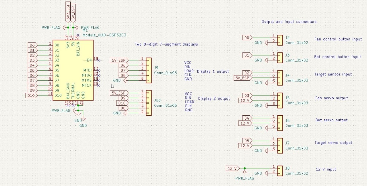
I ran an Electrical Rules Check (ERC) to detect missing connections.

The ERC initially showed an error: "Input power not being driven." I fixed this by adding PWR_FLAGs on the voltage supplies and ground. After this, the ERC ran clean with no errors.
Next I assigned footprints for all the components:

The components with no assigned footprint are highlighted in yellow. The XIAO ESP32-C3 footprint was already available since I used the Fab Academy component library. I manually assigned footprints to the headers. I chose 1mm hole size for the headers, which should be sufficient. Right-clicking a component → "View Selected Footprint" helped me verify that the holes are correctly spaced.

PCB layout design
Next I opened up the PCB editor:

First the PCB needs to be updated from the schematic to bring the footprints of the components defined in the schematic into the PCB editor.
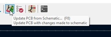
The footprints are initially just side by side like this:
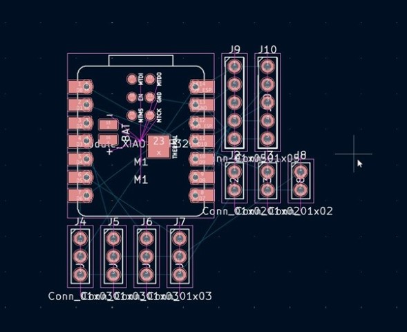
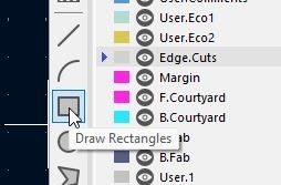
I first drew a preliminary outline for the board cut in the Edge.Cuts layer and later rounded it out by right clicking the outline and choosing Shape modification -> Fillet lines.
Initially, some traces crossed because I was routing on a single-sided board:
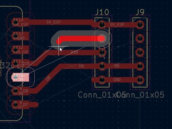
One solution would be to add a jumper (0Ω resistor) to cross the wires, but instead I went back to the schematic and rearranged the pin assignments, as the microcontroller allows flexible output selection.
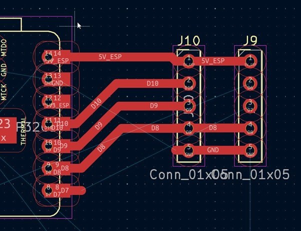
Finally, I created a copper pour connected to the GND pin using the "Draw Filled Zones" tool (Ctrl + Shift + Z) and filled it by pressing B.
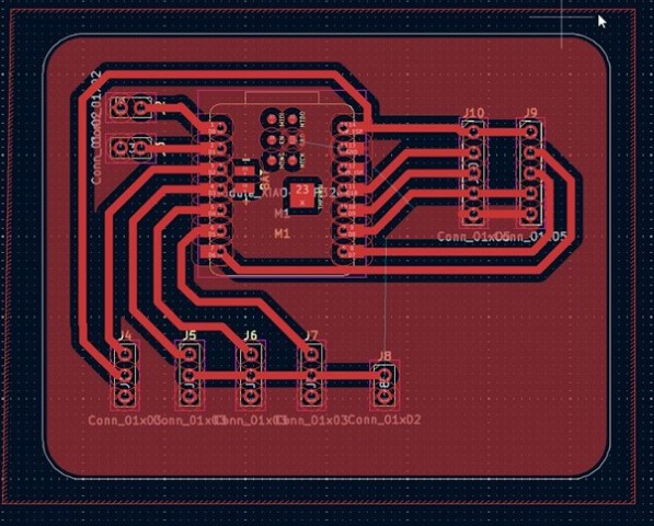
I did a Design Rules Check (DRC) to verify the manufacturability of the PCB. At this stage, the minimum trace width and other constraints are still unknown, as I don't know which manufacturing device I'll be using. I can increase the track width and clearance if needed.
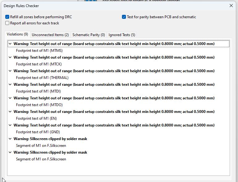
In the Violations tab (image below), I received some DRC errors related to footprint texts and silkscreen overlaps. These don't seem critical.
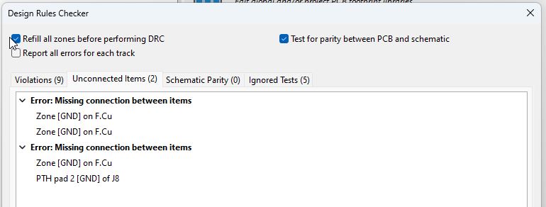
In the Unconnected Items tab, I noticed that a few ground connections were missing. To fix this, I added vias to connect the unconnected GND planes on the top layer to the bottom ground plane of the PCB. After making these adjustments, the DRC check ran clean on the Unconnected Items tab.
Later, I learned that we should only use surface mount devices (SMD) in Fab Academy. Therefore, I replaced the components with SMD footprints and rerouted the PCB. I also added a few decoupling capacitors to the 12 V line. The version 5.3.25 schematic and layout files are listed below, and a 3D render of the PCB can be found in the "hero shot" at the top of this page.
Later on, I changed the footprint of the XIAO ESP32-C3 to fab:Module_XIAO_Generic_SocketSMD to enable the use of SMD sockets for the microprocessor. I also reduced the board outline to provide more space for the connectors.
Exploring AI-Based PCB Design Tools
I briefly checked out flux.ai, which offers AI-assisted PCB design. While it looks promising for larger and more complex circuits, I found that for this simple PCB, manual layout in KiCad is still quicker and more efficient.
Update after week 6:
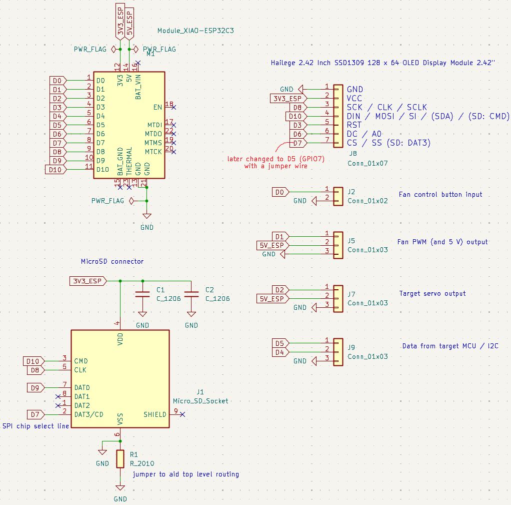
I ended up using the original board as "Board #2" and designed a new Board #1, which includes a microSD card for storing game scores. The schematic for Board #1 is shown below:
In addition, during week 9 I designed and made PCB placed inside the target loop including an "optogate" for ball detection.