In this group assignment, we focused on understanding and documenting the in-house
PCB production process.
Individual Assignment
The individual task was to design, fabricate, and test a custom
microcontroller development board.
Manuel Ayala-Chauvin Institution: Fablab - Universidad Tecnológica Indoamérica Year: 2025
Group Assignment: PCB Production Process Characterization (In-House)
Team: Manuel Ayala-Chauvin, Sandra Nuñez-Torres Institution: Fablab - Universidad Tecnológica Indoamérica Year: 2025
This report presents our group's collaborative experience in characterizing the process of
fabricating printed circuit boards (PCBs) in our lab. We carefully documented key parameters such as
feed rates, spindle speeds, depths of cut, and tooling setups, while also reflecting on the workflow
from start to finish.
Characterization of Design Rules
Parameter
Value
Feed Rate (X/Y)
120 mm/min
Plunge Rate (Z)
60 mm/min
Spindle Speed
10,000 RPM
Cut Depth (Traces)
0.1 mm
Cut Depth (Outline)
0.8 mm
Tooling
V-bit (0.4 mm), End mill (1.0 mm)
Workflow for PCB Manufacturing (Boardhouse)
Create and verify the PCB design.
Generate Gerber files and drill files from the design software.
Validate the files using Gerber viewers.
Submit files to a PCB fabrication service (boardhouse).
Confirm order specifications and make payment.
Receive and inspect fabricated PCBs upon delivery.
PCB Fabrication Process (In-House)
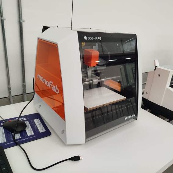
1. Equipment Used: Monofab SRM-20
Our team used the Monofab SRM-20 CNC milling machine, known for its precision on FR-4 or phenolic
copper-clad boards. It proved ideal for our prototyping needs.
2. Initial Test Run
To ensure everything was working properly, we started with a standard test design. This allowed
us to verify the basic setup and machine functionality before moving on to custom designs.
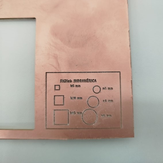
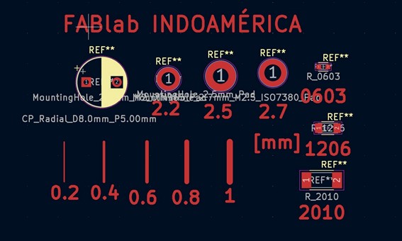
3. Calibration Design Selection
We selected specific calibration patterns from the Fab Academy library. These are designed to
help verify the accuracy and alignment of the machine across small and detailed geometries.
4. Preview and Design Check
As a group, we thoroughly reviewed the PCB design in our CAD software to confirm the geometry was
correct and error-free before exporting.
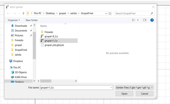
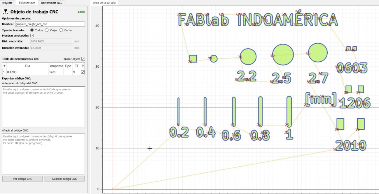
5. Generating Gerber and Drill Files
We exported the required Gerber files for traces and the accompanying drill files. This step was
crucial for preparing the layout for the milling process.
6. File Management
All generated files were saved and organized for easy import into FlatCAM during the toolpath
generation stage.
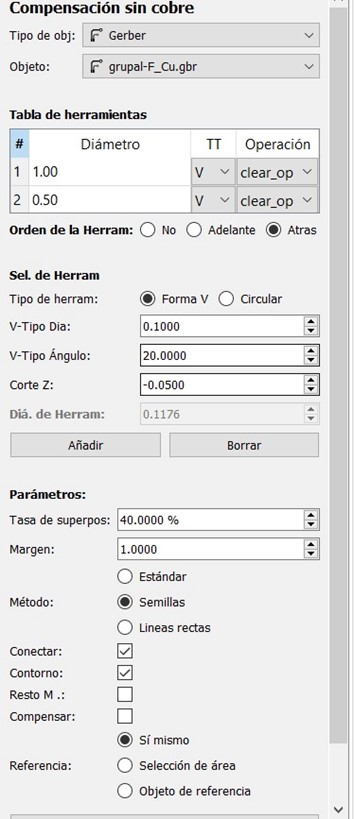
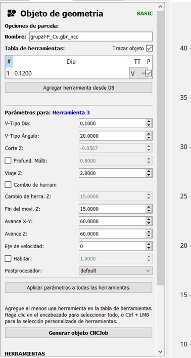
7. FlatCAM Setup
Using FlatCAM, we imported the Gerber and drill files to create toolpaths. This software allowed
us to fine-tune machining parameters before generating the final G-code.
8. Reviewing in FlatCAM
We carefully examined the imported files to ensure trace alignment and correct toolpath
generation.
9. Tool Selection
Our team opted for V-bit tools (typically 0.4 mm) for the trace isolation milling and a 1 mm flat
end mill for the board outline.
10. Machining Parameter Configuration
We configured the CNC settings as follows: 120 mm/min feed rate, 60 mm/min plunge rate, 0.1 mm
depth of cut for traces, 0.8 mm for outline cuts, and spindle speeds ranging from 8000 to 12000
RPM.
11. G-Code Generation
FlatCAM generated the final G-code files, which we saved for use in the SRM-20 milling software.
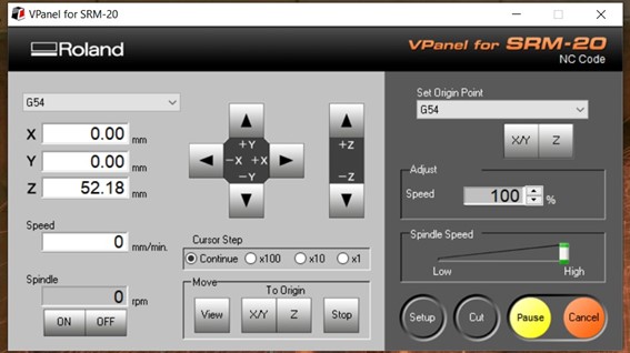
12. Machine Setup on SRM-20
We established the zero point (G54) on the material surface, ensuring alignment before starting
the job.
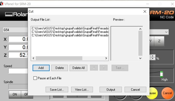
13. Loading Files to the CNC
The previously generated G-code was loaded onto the SRM-20 interface, and we confirmed all
settings matched our defined parameters.
14. Z-Axis Calibration
We carefully adjusted the tool height on the Z-axis using a manual calibration process to ensure
the first layer cut through the copper surface cleanly.
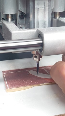
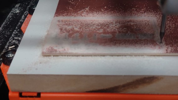
15. Milling Process
The CNC milling process was initiated. Each team member took turns supervising the job, checking
for consistent toolpaths and material removal.
16. Final PCB Output
The result was a clean, precisely milled PCB with accurate traces and a defined board outline,
ready for component soldering.
Conclusion and Group Reflection
This project allowed us to collaboratively explore each stage of the PCB fabrication process. From
design to milling, we gained hands-on experience in toolpath generation, machine calibration, and
file management. We also learned to work as a team, ensuring quality control at every step and
troubleshooting minor issues together. The process enhanced our understanding of digital fabrication
and PCB prototyping workflows.
Design, Fabrication, and Testing of a Development Board with ATtiny412
This project describes the complete process of creating a custom development board using the
ATtiny412 microcontroller. The objective was to cover each stage—from schematic design to
fabrication and testing—allowing for easy replication by students or electronics enthusiasts. The
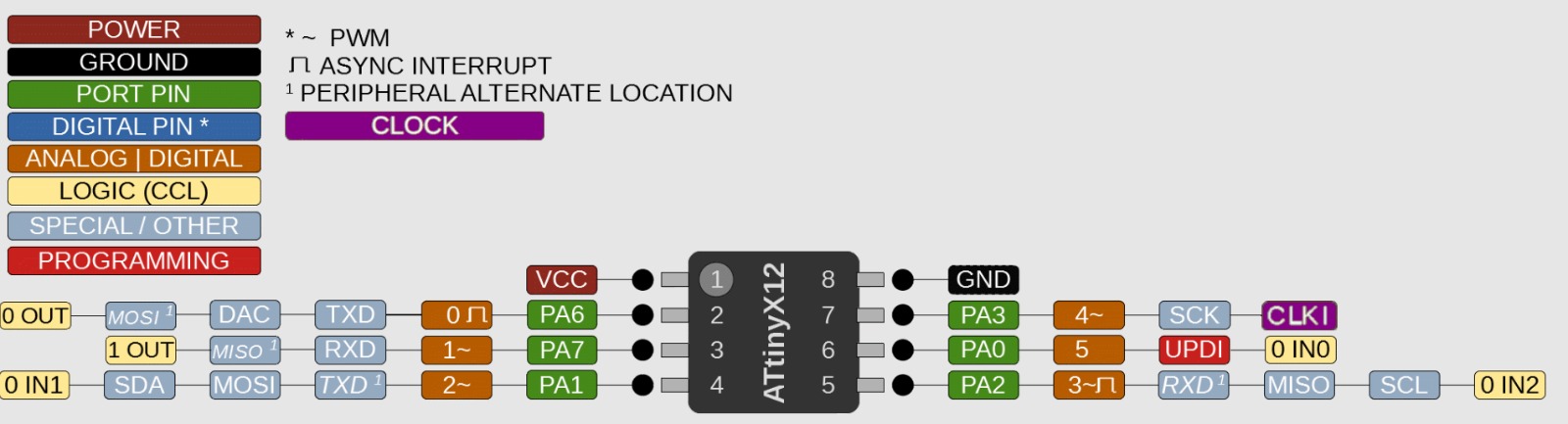
ATtiny412 was chosen due to its compact size, 5V operation, digital/analog I/O, and UPDI programming
interface.
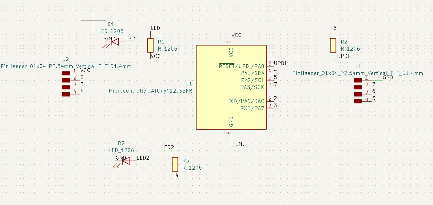
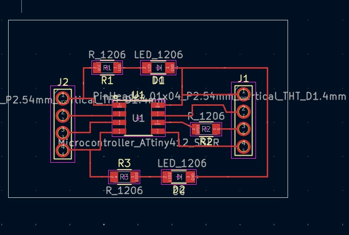
Figure 1: Layout overview of the ATtiny412 custom development board.
The PCB was designed to include a power LED indicator, I/O header pins, a test LED connected to pin
4, and a UPDI port with a programming resistor. The layout was optimized to shorten signal traces
and simplify assembly. Once completed, Gerber and drill files were exported and converted into .nc
format for fabrication using an SRM-20 milling machine.
Figure 2: Electronic schematic of the board, highlighting component connectivity.
Figure 3: Component layout optimization for better routing and compact design.
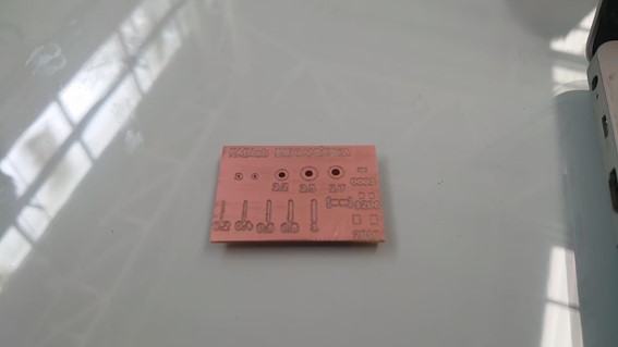
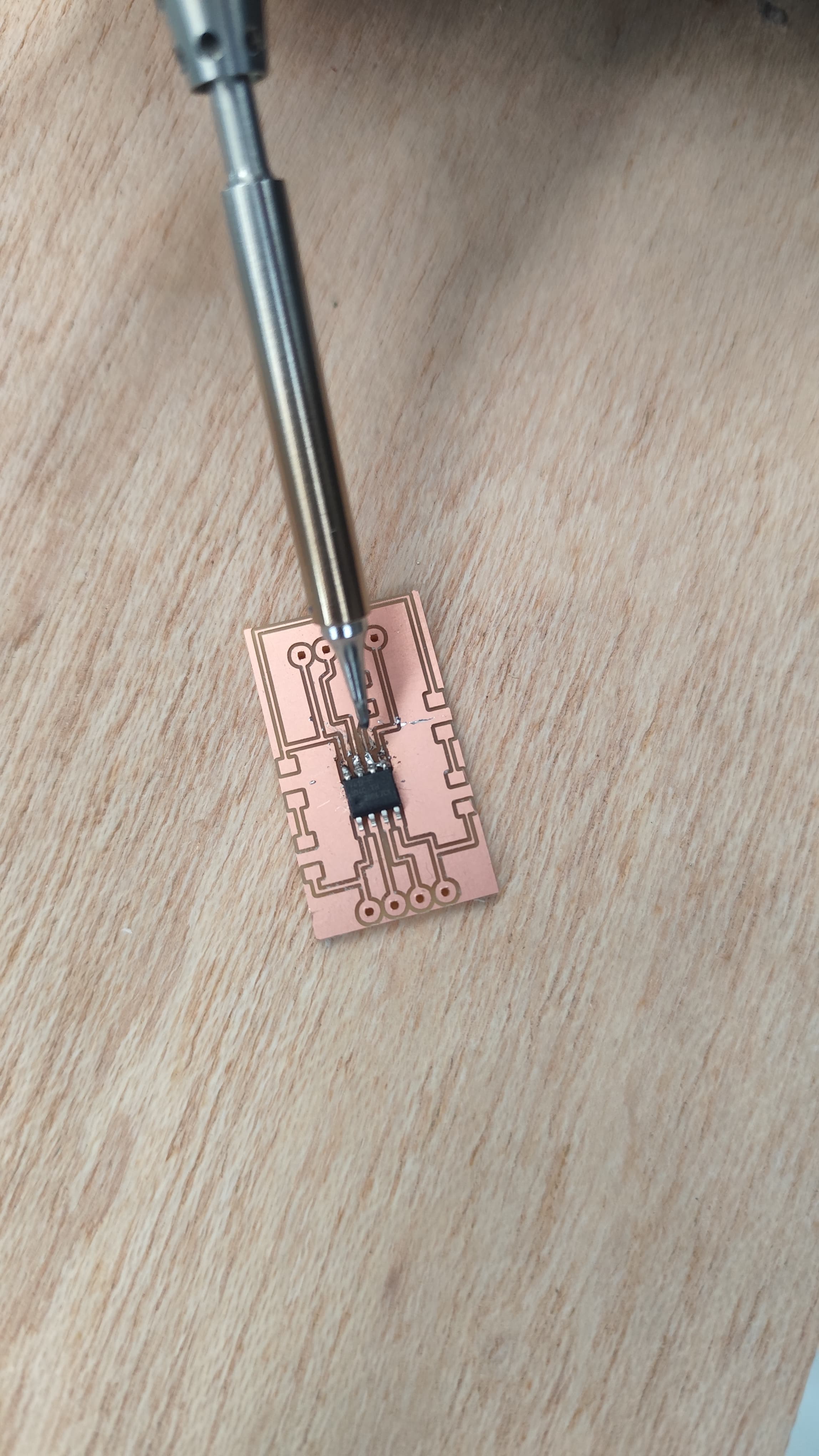
With the board fabricated, components including the ATtiny412, resistors, and LEDs were soldered onto
the PCB. A continuity test confirmed that all traces were correctly isolated and no shorts were
present.
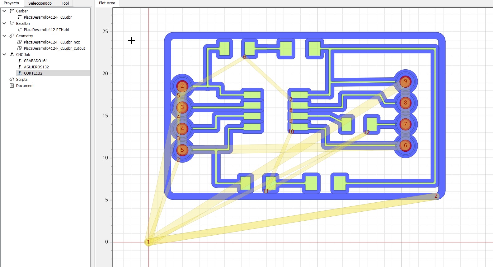
Figure 4: Interface used for generating milling paths for the SRM-20.
Figure 5: SRM-20 milling machine configured and ready for PCB fabrication.
Figure 6: Fully assembled ATtiny412 board after component soldering.
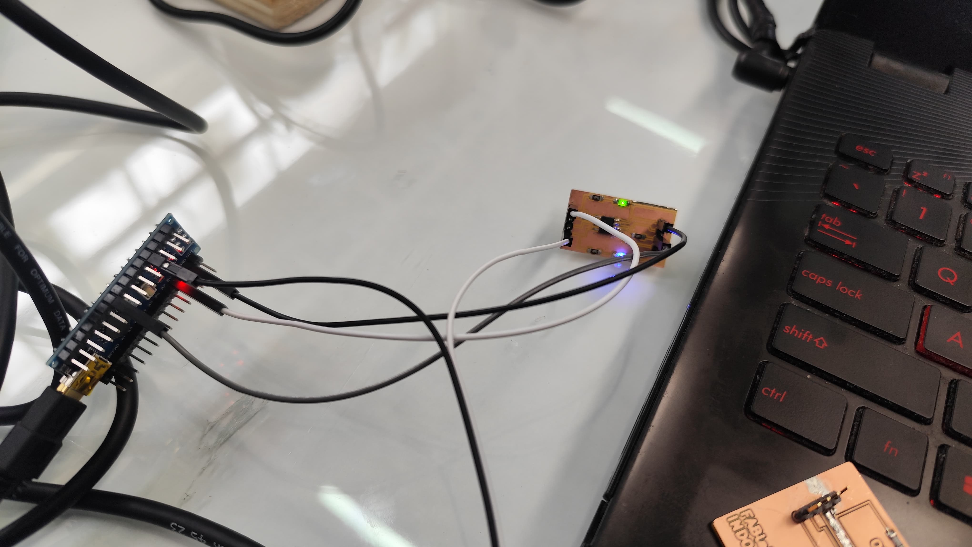
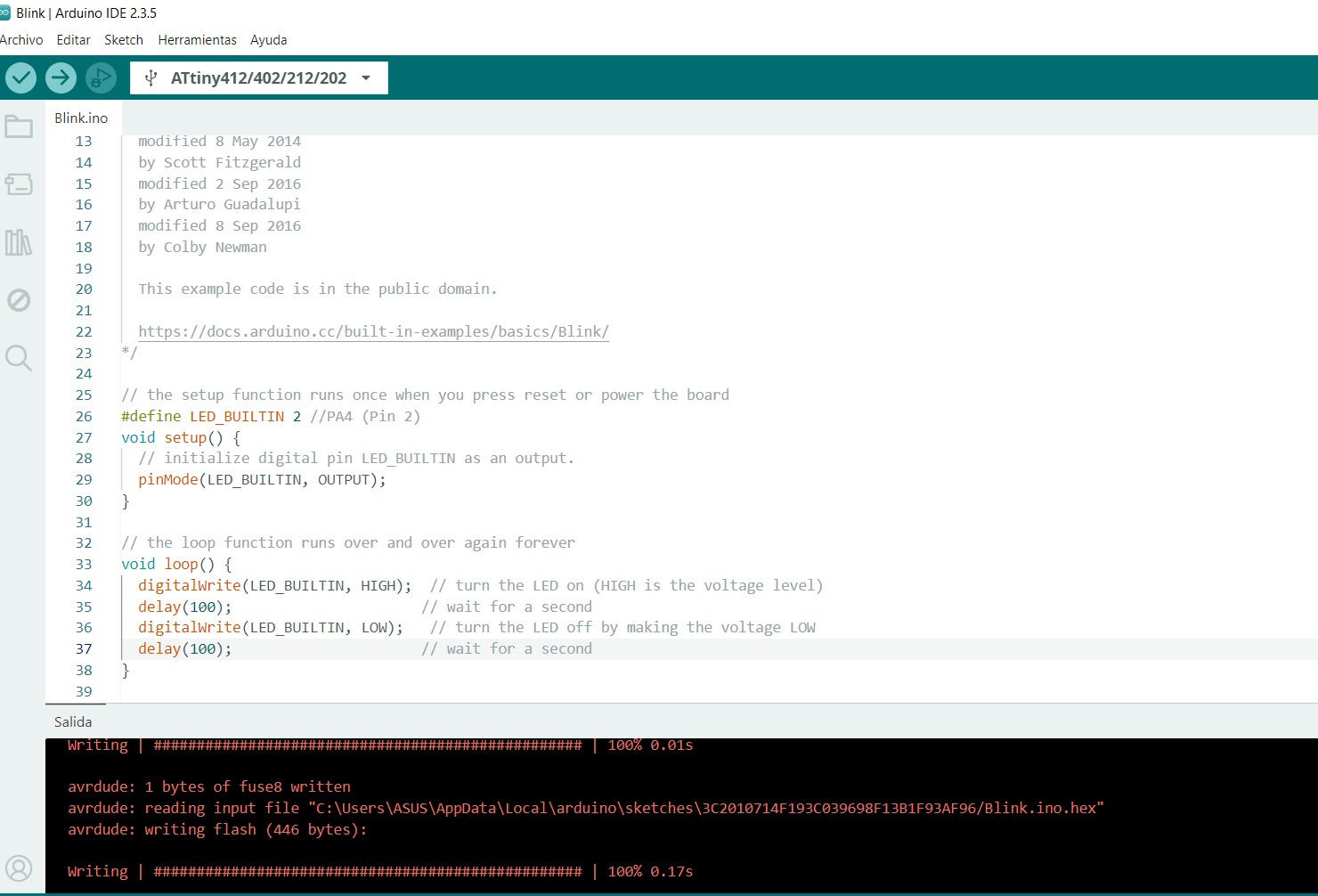
To program the board, an Arduino Nano was configured as a UPDI programmer. A test program was
uploaded to the ATtiny412 to blink the test LED on pin 4, confirming correct operation and
successful programming.
Figure 7: Programming setup using Arduino Nano as a UPDI programmer.
This hands-on project covered the entire workflow of developing a microcontroller board,
including
electronic design, manufacturing, and embedded programming. The result is a replicable and
educational prototype, ideal for both learning environments and DIY electronics experimentation.
Week 8: Conclusion
During Week 8, I gained comprehensive knowledge and hands-on experience in electronics
production, both at the group and individual levels. As a team, we successfully characterized
the in-house PCB production workflow, from the initial calibration tests to the fine-tuning of
parameters and final milling operations. This collaborative process deepened our understanding
of CNC milling techniques and the importance of precision in electronics fabrication.
Individually, I designed, manufactured, and programmed a functional development board using the
ATtiny412 microcontroller. This task enhanced my skills in schematic design, layout
optimization, milling preparation, soldering, and embedded programming. Programming the board
and testing it through a simple blinking LED program served as a tangible confirmation of the
board's functionality.
Overall, this week was a valuable opportunity to bridge theory and practice in digital
fabrication and electronics, building foundational skills for future embedded systems projects.
Resource Download
Click the button below to access and download all available materials.