- Group Assignment
- Observation of the Operation of a Microcontroller Board
- Individual Assignment
- Design of a Development Board Using an EDA Tool.
Manuel Ayala-Chauvin
Institution: Fablab - Universidad Tecnológica Indoamérica
Year: 2025
Manuel Ayala-Chauvin
Institution: Fablab - Universidad Tecnológica Indoamérica
Year: 2025
Team: Manuel Ayala-Chauvin, Sandra Nuñez-Torres
Institution: Fablab - Universidad Tecnológica Indoamérica
Year: 2025
We analyzed a basic circuit using an Arduino UNO, a red LED, a resistor, and a breadboard. The LED was observed to be ON, confirming that the circuit was correctly powered and functional.
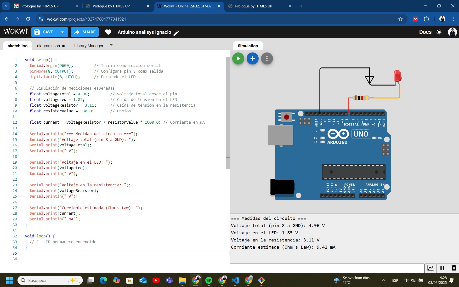
| Measured Parameter | Obtained Value |
|---|---|
| Voltage at Arduino digital output (control pin) | 4.96V |
| Voltage across LED (anode-cathode) | 1.85V |
| Voltage across resistor | 3.11V |
| Current through LED (calculated with Ohm's Law) | 9.42 mA |
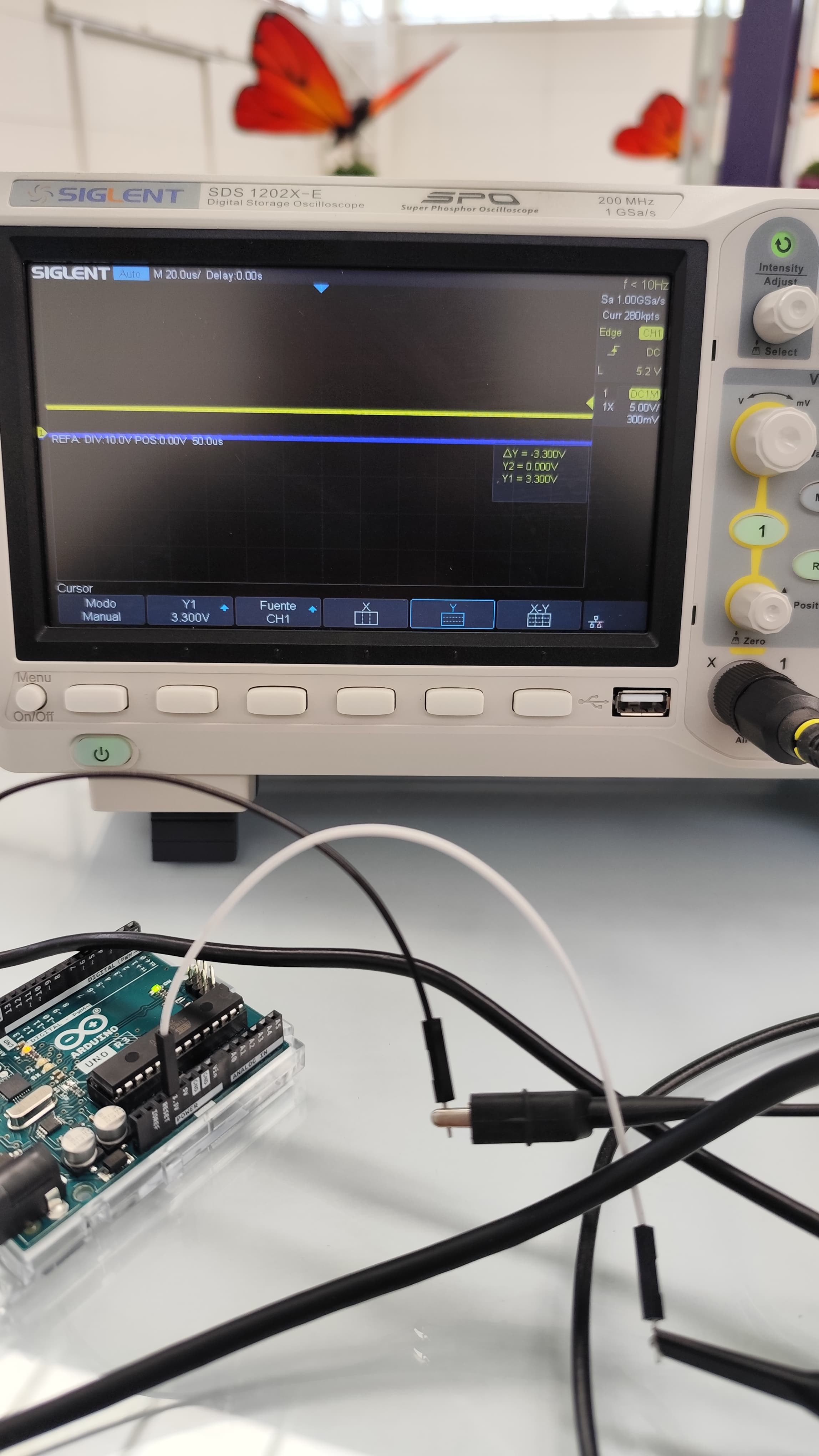
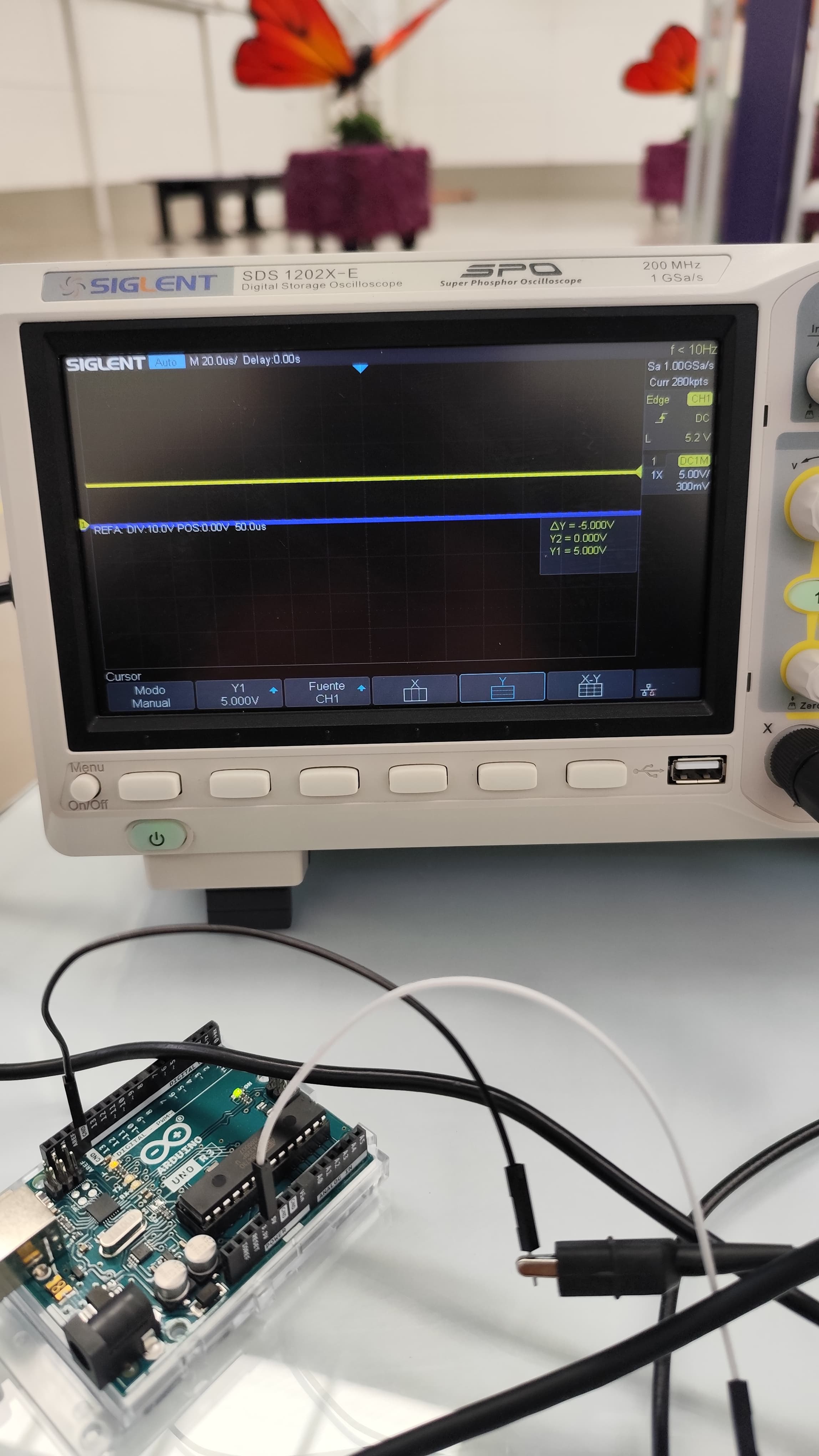
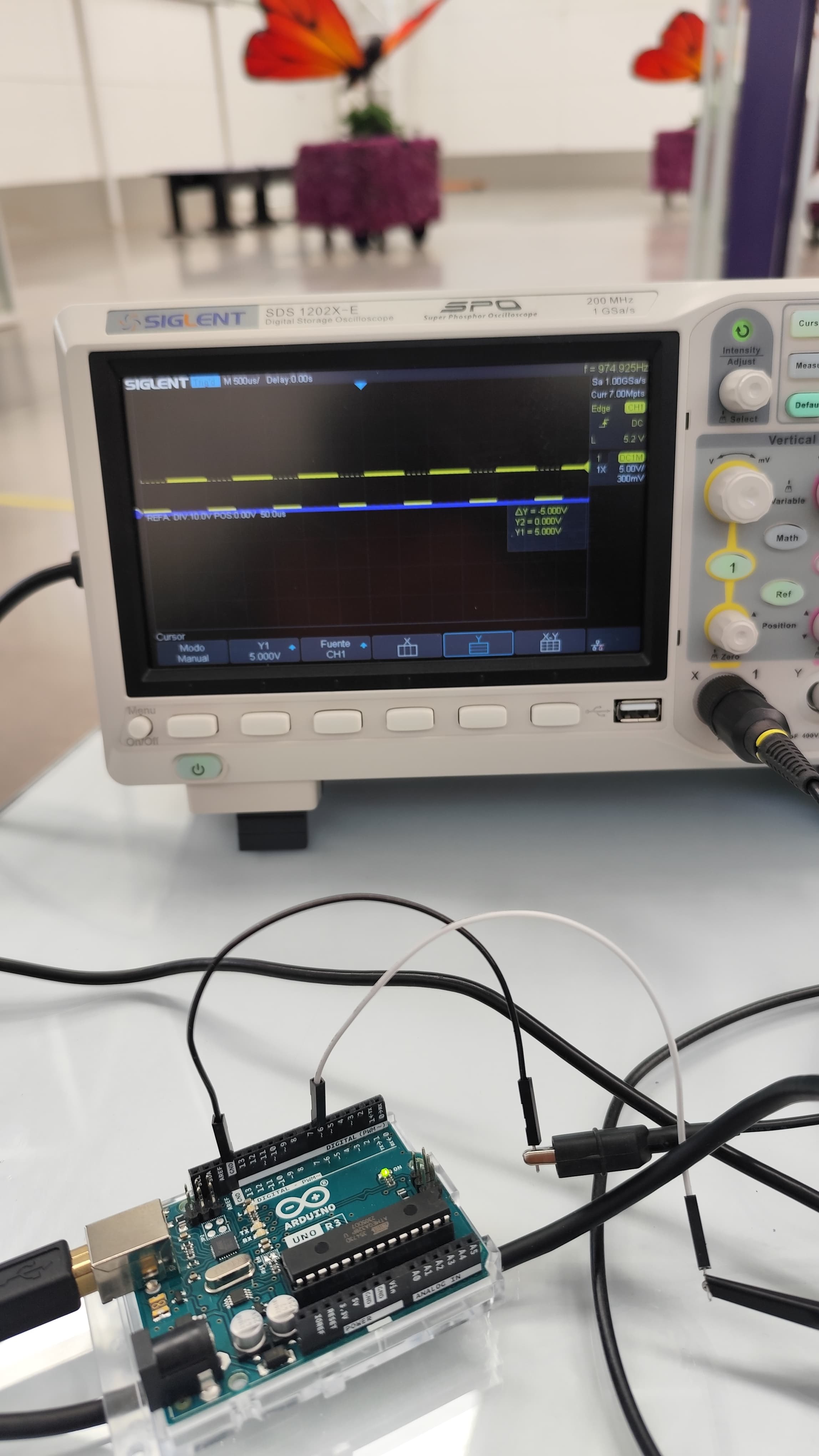
The goal is to use the oscilloscope to visualize the PWM signal generated by Arduino. This demonstrates how the duty cycle of the signal changes over time, affecting the LED brightness.
The images show an experiment using an Arduino Uno and a Siglent SDS 1202X-E oscilloscope to observe the PWM signal generated by the microcontroller.
The oscilloscope displays a flat line at 3.3V, indicating that the measured pin is in a constant HIGH state (no PWM modulation visible yet).
The oscilloscope shows a 5V signal, meaning the measured pin is in HIGH state without variations.
A pulsed (PWM) signal appears, with transitions between 0V and 5V. This confirms that Arduino is correctly generating the PWM signal.
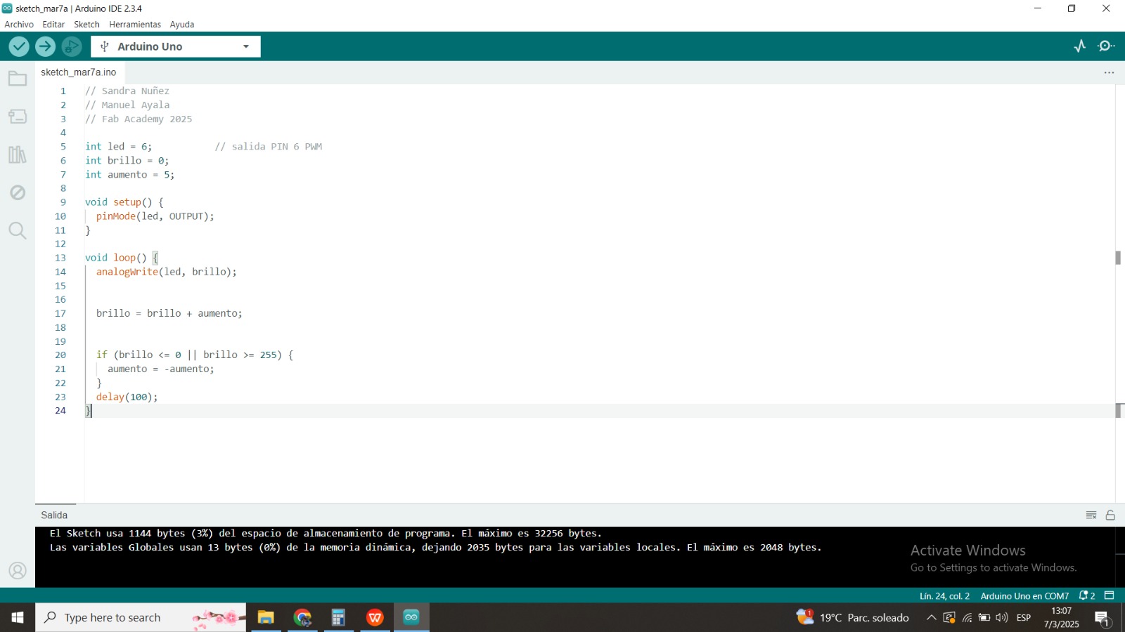
The Arduino code implements a progressive fading effect on an LED connected to pin 6 using PWM (Pulse Width Modulation).
led = 6; → Defines pin 6 as the LED output.brillo = 0; → Stores the LED brightness level (PWM value from 0 to 255).aumento = 5; → Defines how much the brightness increases or decreases in each
iteration.setup)pinMode(led, OUTPUT); → Configures pin 6 as an output.
loop)analogWrite(led, brillo); → Sends a PWM signal to the LED.brillo = brillo + aumento; → Increases or decreases brightness.aumento direction is
reversed.delay(100); → Waits 100 ms before the next update.The LED gradually increases in brightness until it reaches the maximum (255). Then, it gradually dims until it reaches 0. This cycle repeats indefinitely.
Click the link below to download the Arduino code:
PwmLED.inoThe circuit functions correctly based on the performed measurements. The LED receives the appropriate voltage, and the current remains within the recommended limits. Further testing could involve programming variations in the Arduino output signal and using an oscilloscope to visualize the waveform.
The goal of this assignment is to design a custom development board using an EDA (Electronic Design Automation) tool, incorporating components from the inventory and enabling interaction and communication with an embedded microcontroller.
For this project, the following components were selected:
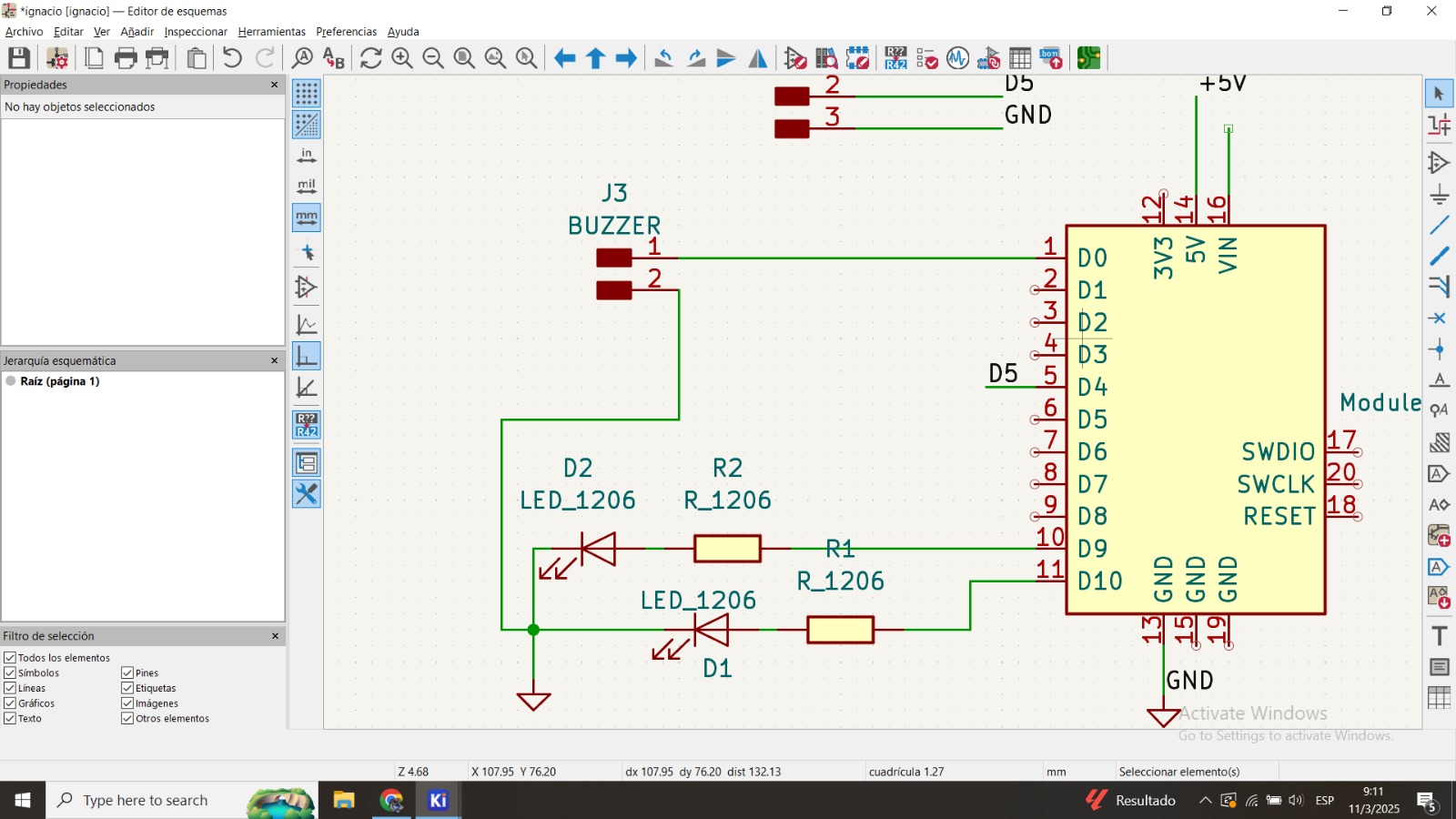
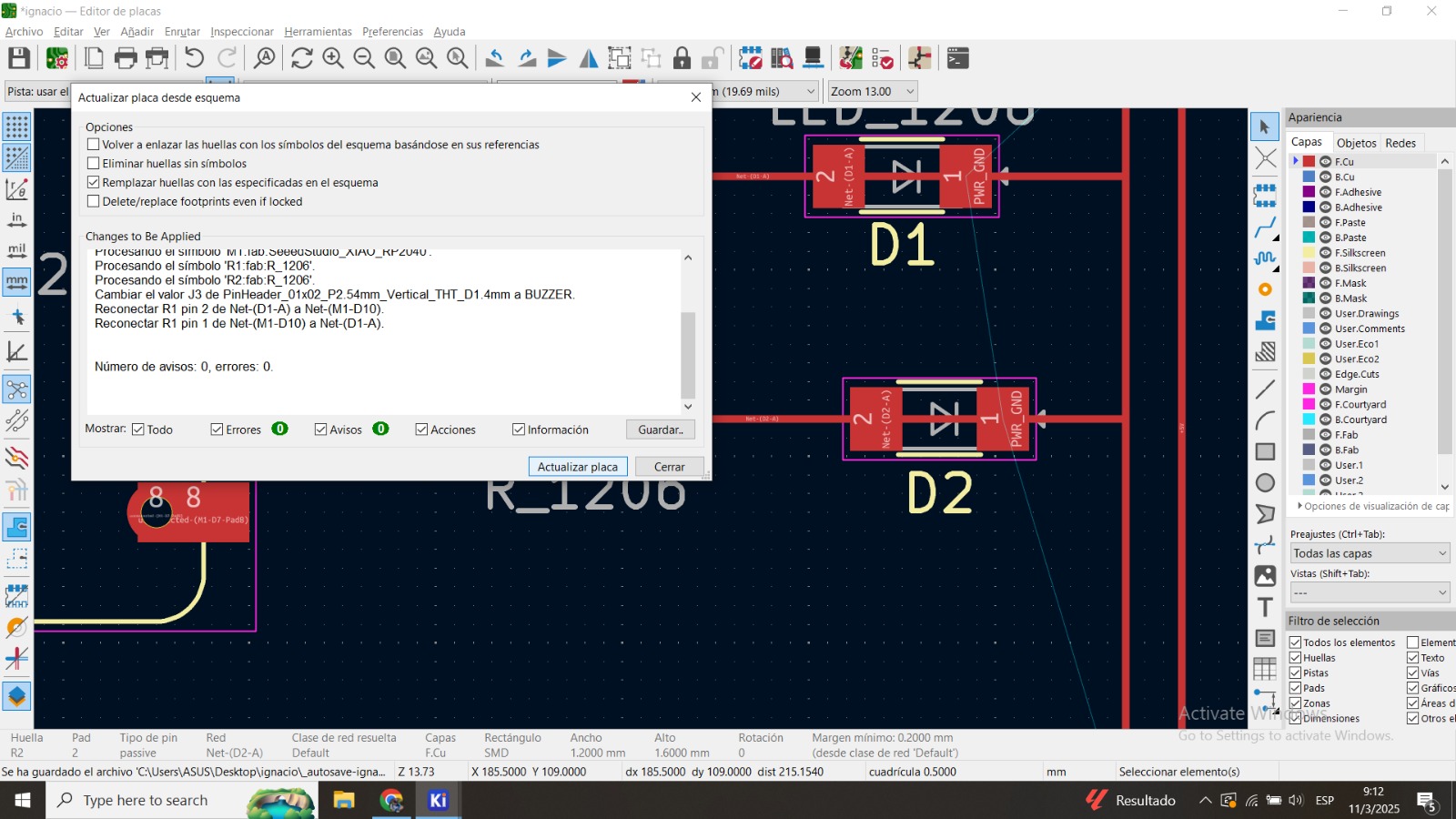
Using KiCad, the schematic was designed with:
The schematic was created in KiCad, ensuring proper electrical connections and component placement.
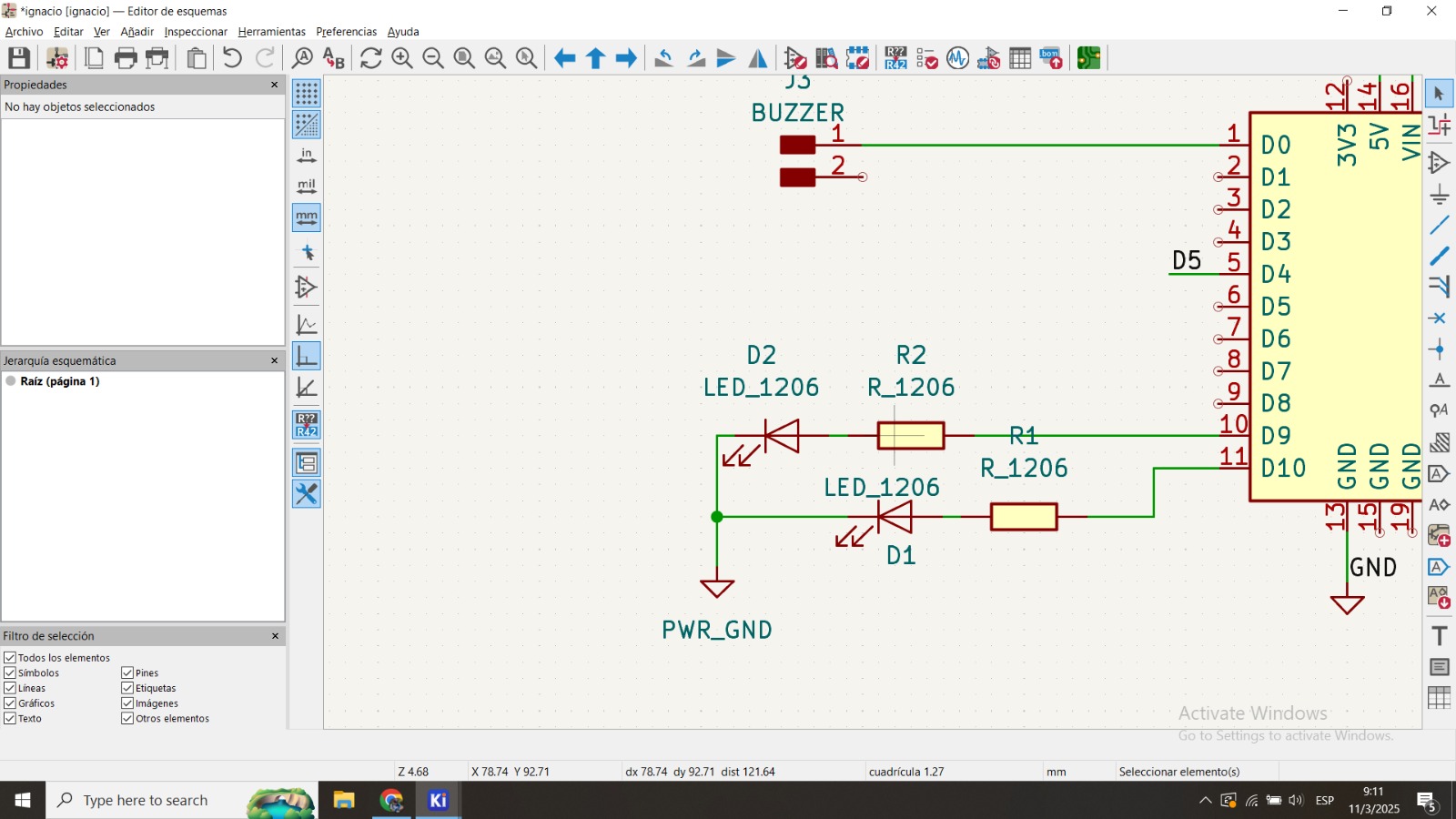
This circuit operates by using digital pin D5 of the microcontroller, which when set to HIGH allows current to flow to both a buzzer and two LEDs connected in parallel. Each LED is paired with a limiting resistor (R1 and R2) to protect the components from excessive current. When D5 is HIGH, the LEDs turn on and the buzzer emits sound, providing both visual and audible indication that the system is active. When D5 is set to LOW, the current is cut off, turning off the LEDs and silencing the buzzer, indicating the system is inactive.
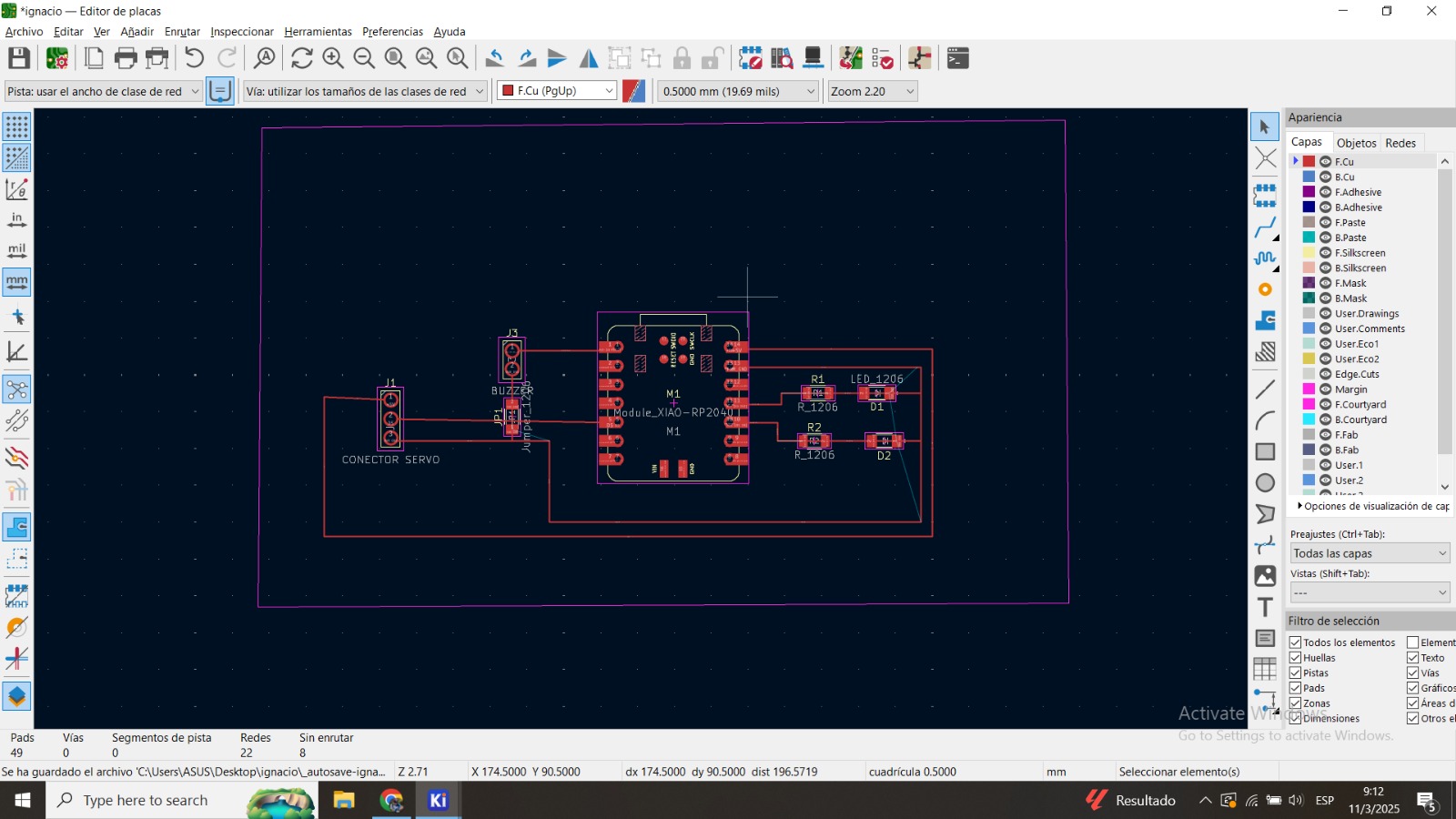
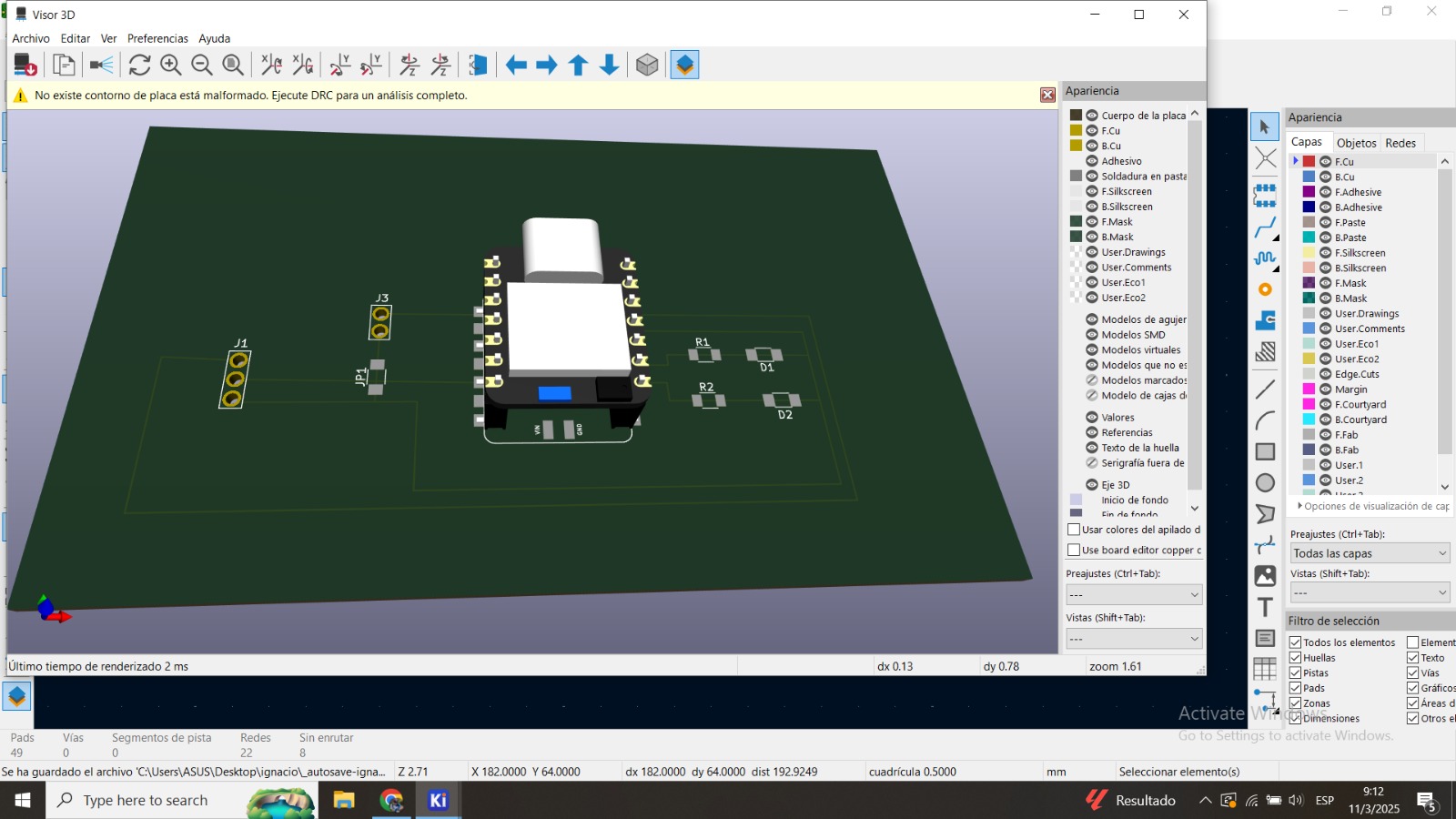
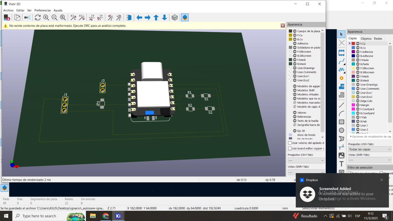
After verifying the schematic, the PCB layout was designed:
The placement of components ensures short signal paths, proper spacing, and clearances for manufacturability.
A 3D render of the PCB was generated to inspect the component placement and board design.
Final adjustments included:
The board is ready for fabrication and assembly. Further improvements could include:
The design meets the project requirements for embedded microcontroller interaction and peripheral communication.
This project provided a hands-on approach to designing a custom development board using EDA tools. It enhanced skills in:
This week was a valuable opportunity to deepen my understanding of electronic circuit design and analysis. Through the group assignment, I explored the behavior of a microcontroller-based circuit using an Arduino UNO, performed voltage and current measurements, and observed PWM signals through an oscilloscope. This provided a hands-on understanding of how microcontrollers interact with external components and how to properly analyze signal characteristics in real-time.
For the individual assignment, I used KiCad to design a custom development board that integrates a microcontroller, status LEDs, a buzzer, and a connector for a servo motor. The process included schematic creation, PCB layout design, 3D visualization, and validation through design rule checks. This exercise helped me strengthen my skills in EDA tools, component integration, and PCB manufacturing preparation.
Overall, this week enhanced my proficiency in both the theoretical and practical aspects of electronics design, setting a solid foundation for future assignments and the final project development.
Click the button below to access and download all available materials.
Download Resources