Characterize the design rules for your in-house PCB production process: document feeds, speeds, plunge rate, depth of cut (traces and outline) and tooling.
Document the workflow for sending a PCB to a boardhouse
Document your work to the group work page and reflect on your individual page what you learned
Individual Assignment:
Make and test a microcontroller development board that you designed
Have you answered these questions?
Linked to the group assignment page ✅
Documented how you made the toolpath ✅
Documented how you made (milled, stuffed, soldered) the board ✅
Documented that your board is functional ✅
Explained any problems and how you fixed them ✅
included a ‘hero shot’ of your board ✅
Group Assignment
Characterize the design rules for your in-house PCB production process: document feeds, speeds, plunge rate, depth of cut (traces and outline) and tooling.
Document the workflow for sending a PCB to a boardhouse
Document your work to the group work page and reflect on your individual page what you learned
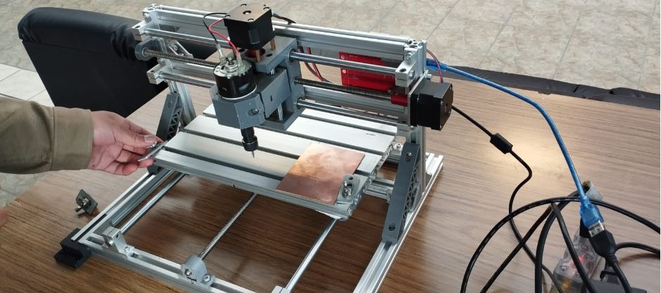
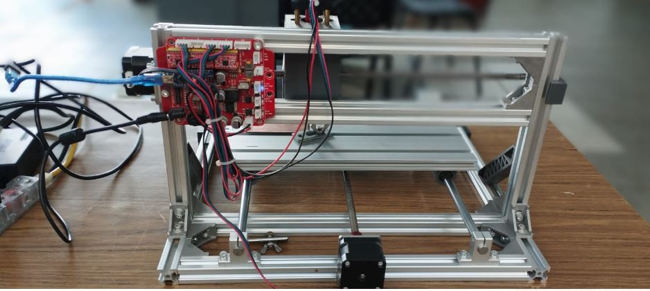
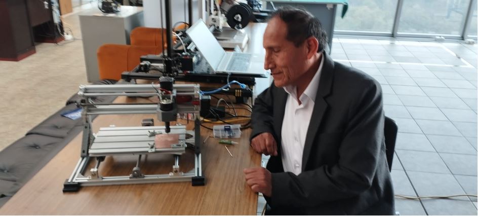
The group project was carried out at the UNCP Fab Lab. We used a small CNC-PBC machine in this lab. Initially, it presented some problems, such as looseness in some of the engine mount bolts. We had to make some adjustments and also install the finest 0.1 mm and 0.2 mm cutters. We then used the CNC milling machine and performed some initial motion tests.
Motion testing on CNC PCB (printed circuit board) milling machines is essential to ensure the equipment's accuracy, repeatability, and safety before milling the board. In addition, no-load testing is also essential to verify that the axes move according to the programmed path.
Reflections
During the process of making the board as an exercise, it was not complicated, but I had to do some tests before working the milling process with the real board, the movement tests, the displacement, as well as the calibration of the X,Y,Z axes were essential to ensure the displacement of the axes with precision and thus obtain better results for the manufacturing of our PCB.
The PCB manufacturing process with PCBWay is quite simple and automated, ideal for both prototypes and mass production. You just need to have the file ready in the software being used for the design, in our case kiCAD, and then generate a manufacturing file called Gerber. This file is then uploaded to the PCBway website where you can enter various data such as the number of layers, dimensions, PCB thickness, among others. I think it's a good option, but production using our own CNC PCB machines is even better.
Individual Assignment
Make and test a microcontroller development board that you designed
extra credit: make it with another process
To carry out the PCB manufacturing process, we will use the electronic design worked on in the Kicad software, the same one that was made during week 6. First, we will show the arrangement of the components in the 3D view and then we will detail the steps we followed to manufacture our PCB.
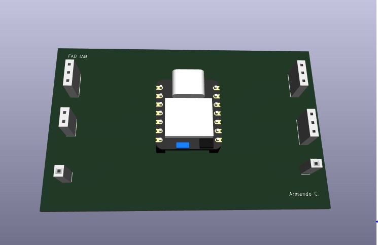
View of the PCB components
The 3D view shows the PCB electronic components
The 3D view of the top layer allows us to see the layout of the components on the designed board and see what it would look like once the PCB is manufactured.
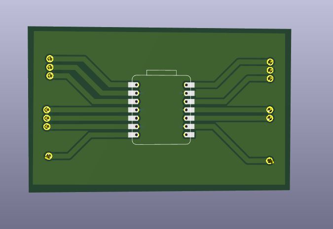
3D view of the bottom layer
The 3D view of the bottom layer allows us to see the traces drawn on the designed board and see what it would look like once the PCB is manufactured.
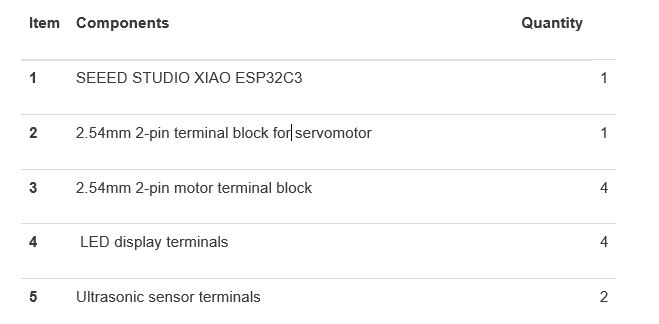
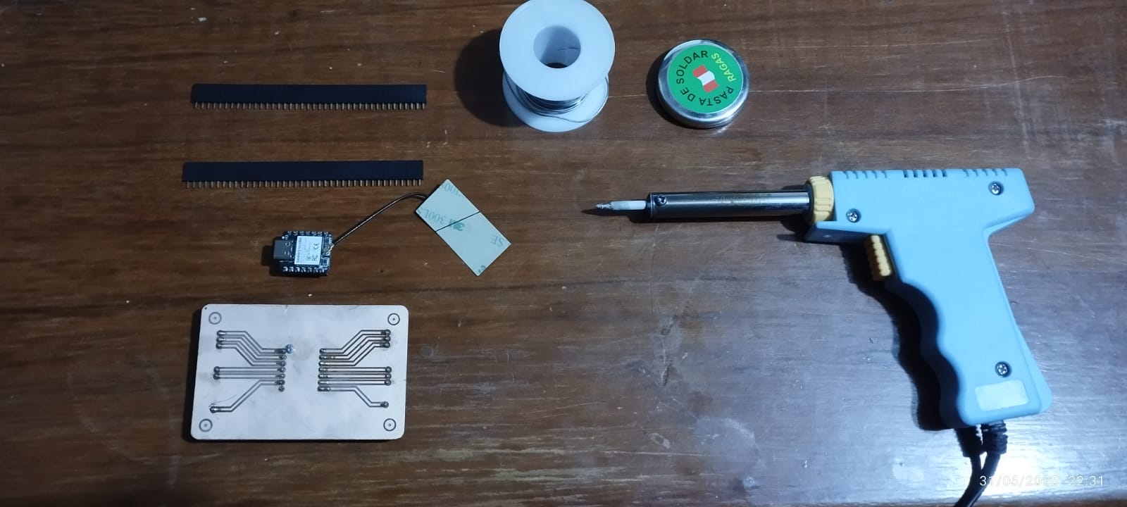
List of materials to be used
The 3D view shows the PCB electronic components
Making the PCB
The steps to follow are as follows: download the Gerber file generated in KiCad and then import it into FlatCAM, a free and open-source application that allows you to take your designs to a CNC mill. You can open Gerber, Excellon, or G-code files, edit them, or create them from scratch and generate G-code. Isolation routing is one of the many tasks FlatCAM is perfect for; it's written in Python and runs smoothly on most platforms.
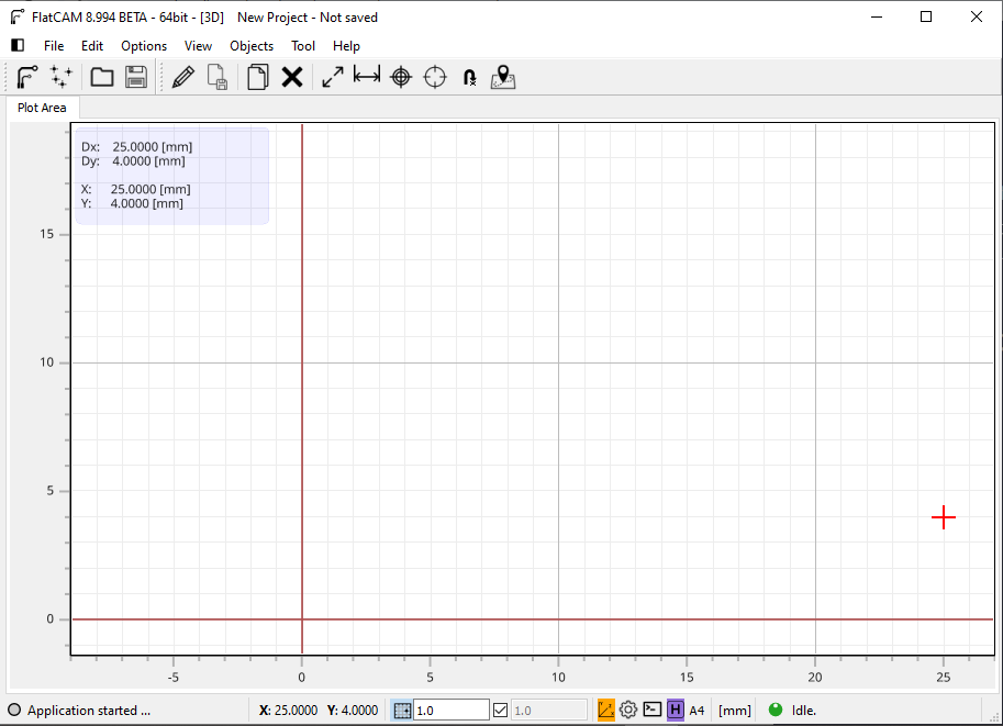
Open the FlatCam 8.994 BETA Program
Launch the FlatCAM application
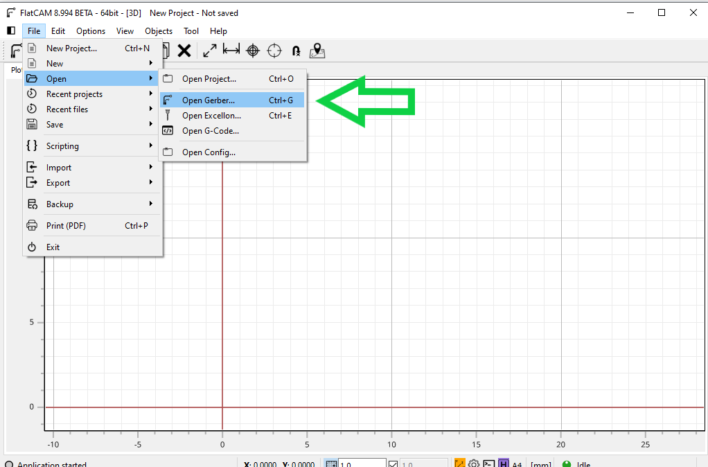
Import the Gerber File
Go to the File menu and open the Gerber file generated in Kicad as a manufacturing file.
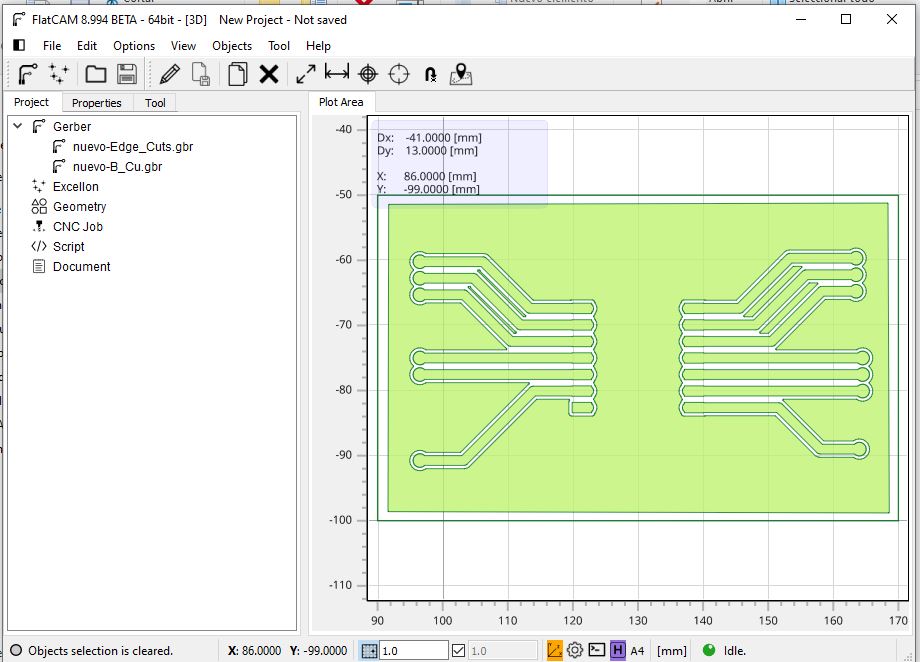
software FlatCam 8.994 BETA
Our Gerber file was imported into FlatCAM
Tool Path Generation
In FlatCAM, toolpaths are the paths that the milling cutter or drill bit will follow on the CNC machine to create the PCB. These are generated from Gerber files (for copper, masks, etc.) and Excellon files (for holes).
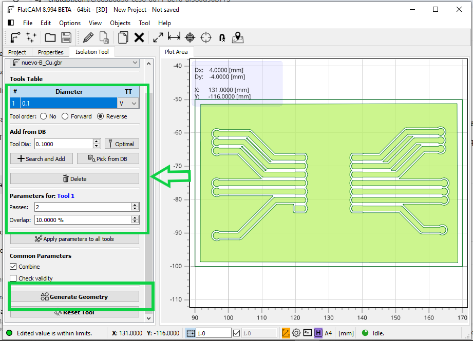
Isolation Routing
This path eliminates copper around the tracks, To do this, go to Project and select a Gerber file, in this case the layer below. In the "Isolation Routing" section, configure: Tool dia (milling cutter diameter): 0.1 mm, number of passes: 2. Pass overlap: % overlap between passes: 10%. Then, click to generate the geometry.
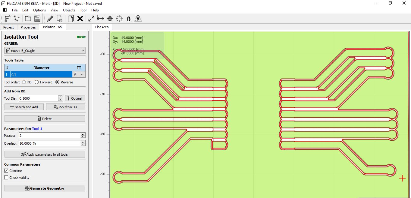
Geometry Generation
A new geometry file will be created
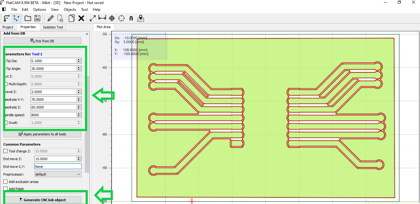
Generates G-code of the Insulation
In this option we view the parameters for the tool, in this case the 0.1mm cutter, with an angle type of 30°, "XY" speeds of 70mm/s, "Z" at 60mm/s, then click on apply parameters and the next step is to click on Generate Job.
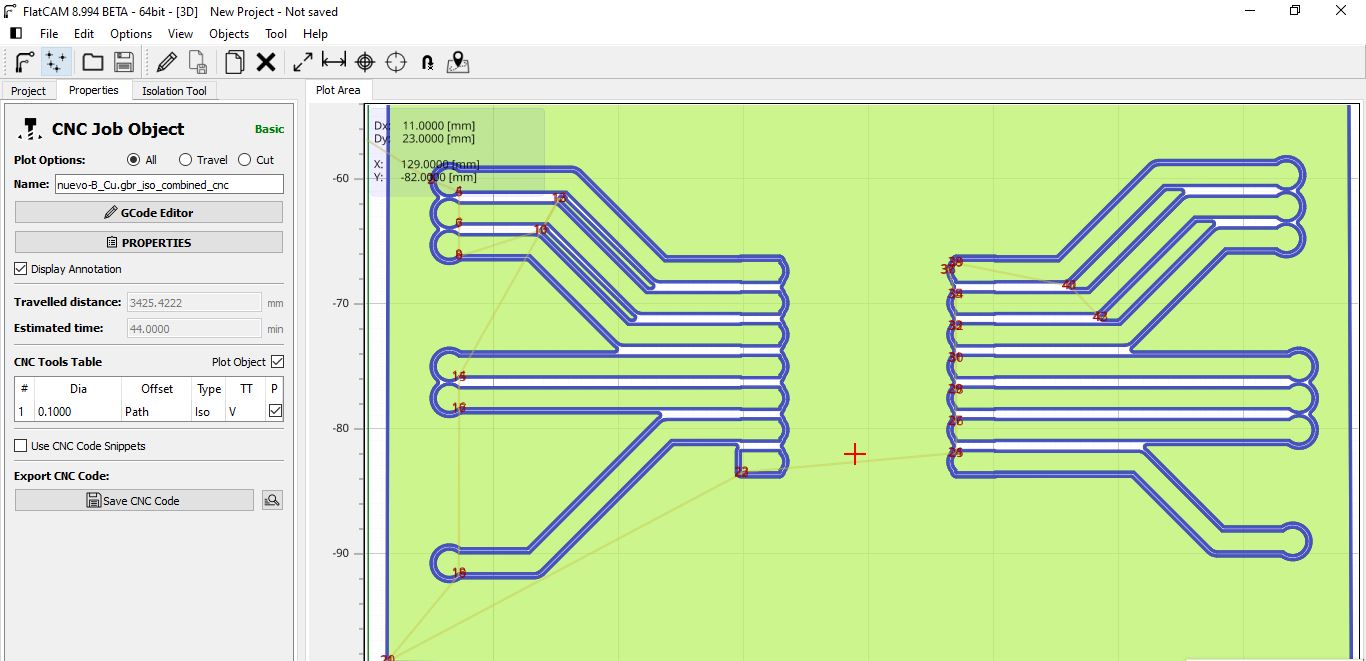
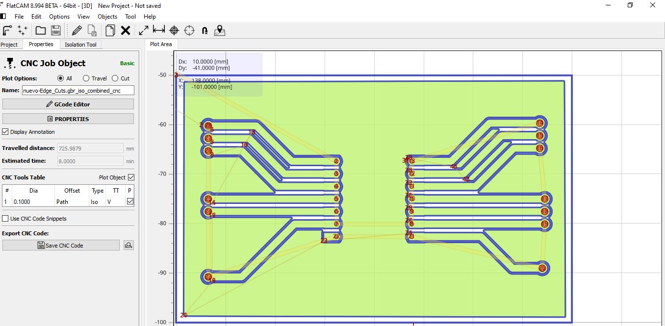
CNC Job Object
Once the insulation, cutout and copper cleaning paths have been completed, the work object is generated, where the G-code file that the CNC machine will execute can be generated.
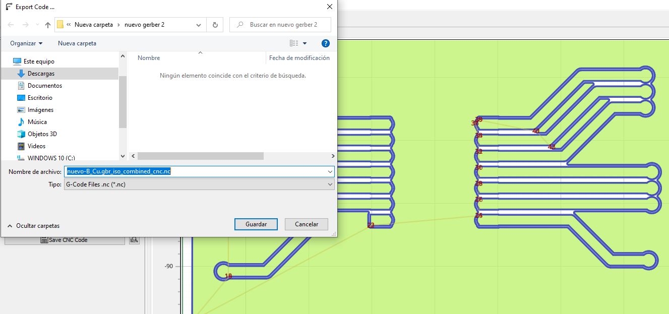
Save the Generated G-code
Once you have generated the CNC Job Object in FlatCAM and verified it, the last step is to save the G-code to a destination folder for use on your CNC machine.
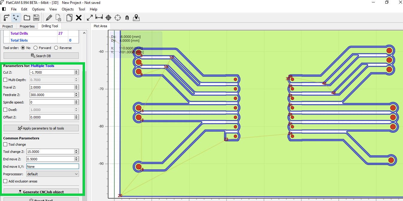
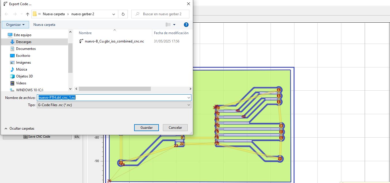
Generating G-code for Drilling in FlatCAM (final step)
We open the Excellon file, which contains the perforations of our card, the .drl file, is one of the files that is generated for manufacturing.
Configure CNC Job Parameters
We set the drilling parameters: 0.8 mm (drill bit used), Z travel 1.0 mm, and Z feed rate 60–120 mm/min.
We save the G-code file
After configuring the parameters, click Generate, and flatCAM will create a new CNC Job object. We'll save it in a destination folder with the G-code file for the holes, ready to load into the CNC machine and drill the holes in the PCB. These files are saved separately.
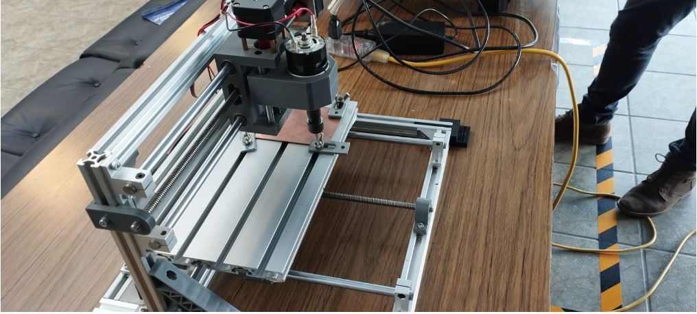
The next step is to firmly position the Bakelite substrate on the CNC machine bed and begin milling the PCB tracks. Ensuring a firm and stable hold of the Bakelite is crucial to achieving optimal precision throughout the milling process. Once started, the CNC machine will execute the G-code file instructions to accurately mill the tracks according to the previous design.
Plate to be placed on the PCB
Here is the plate to be placed on the PCB.
Board fixed on the PCB
The image shows the board fixed to the PCB, it is held in place by 04 fasteners to prevent the board from moving.
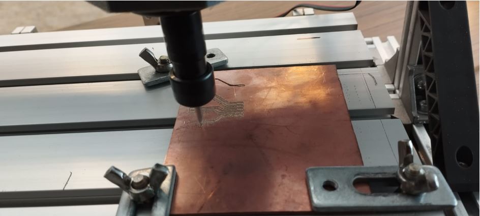
Printing lines
In this process we can verify the printing lines that the PCB is making.
Printing lines
We continue checking the printing lines that the PCB is making. In this case, the time will be approximately 10 minutes.
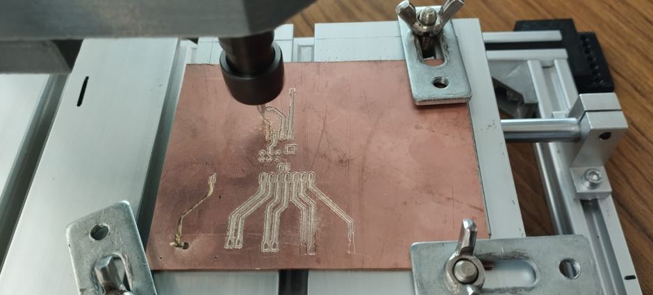
Here we see the progress of the printing lines; we are almost halfway there
80% progress
Did you have any problems?
Yes, I had an error adjusting the motor support, since it was not adjusted properly, which caused a faulty trajectory. The machine was stopped to correctly adjust the cutter, a new coordinate was given and the corresponding trajectory started.
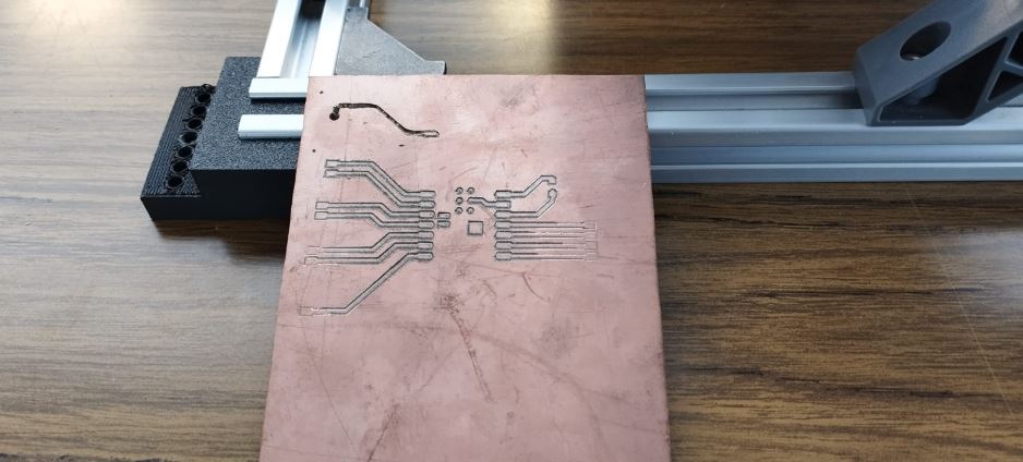
Finished impression
In this first test we did not have good results, since some tracks were not well traced, so we performed a second CNC machining of our PCB design.
The plate is shown with the aforementioned errors
Due to the errors we had in the first test of the plate printing, which was displayed on said plate, this had to be corrected by performing a second test, with the configuration of the tool mentioned above, which had a satisfactory result which is shown in the following figure.
Second CNC machining of the PCB
For this second test we had better results, since the leveling of the PCB surface was checked and automatic Z height tests were performed.
Two cards were made to see the quality of each one.
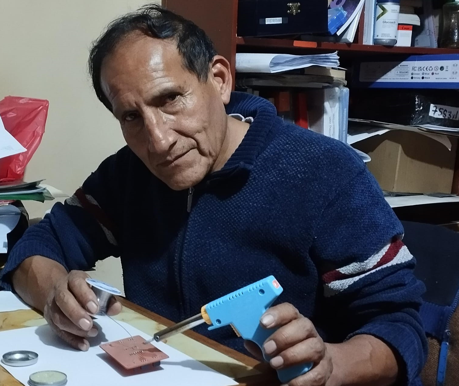
Soldering process of components on the PCB
Components we will use
The components to be used are the following: Bakelite, tin, solder paste, single-row female connector with a 2.54 mm vertical through hole and solder pad.
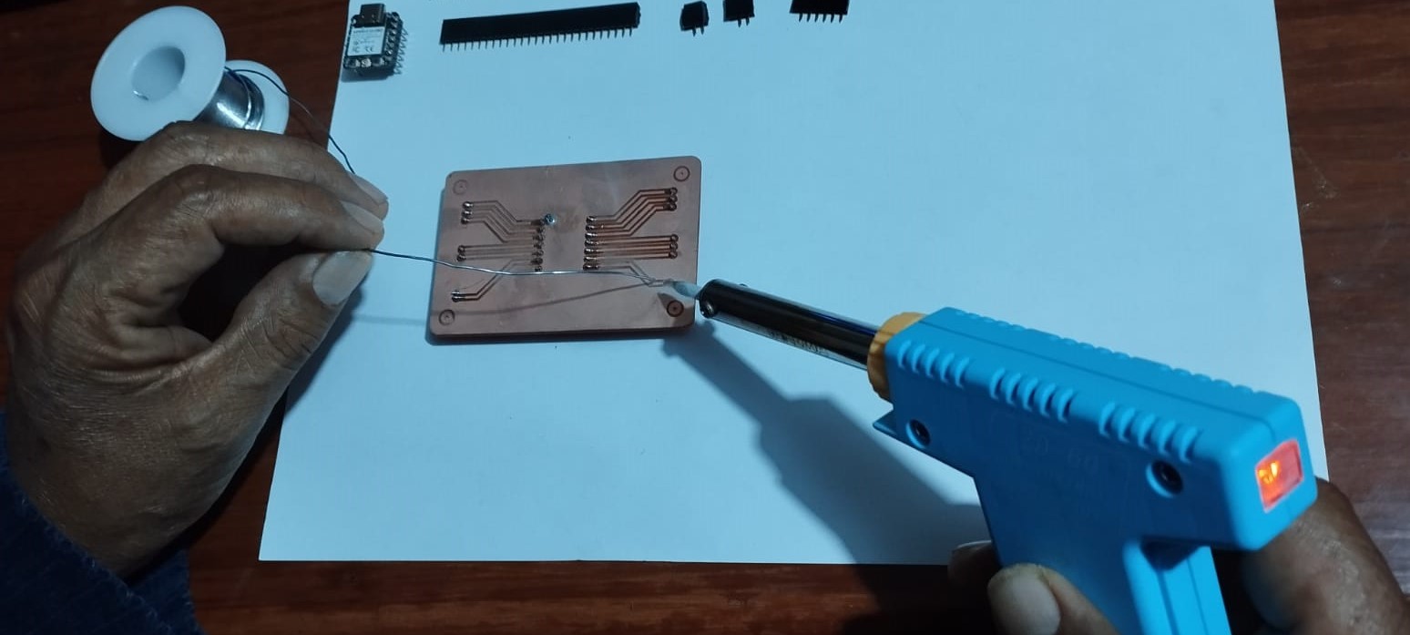
Proper welding process
We heat the pin and the track simultaneously by applying the soldering iron tip where they touch. After 1-2 seconds, apply the solder to the contact point (not directly to the soldering iron tip).
For the soldering process: A fine-tip soldering iron (350–400 °C) was used, then a flux-cored leaded solder wire (60/40 Sn-Pb) was applied to each pad. The through-pin headers were placed in their respective positions and carefully soldered.
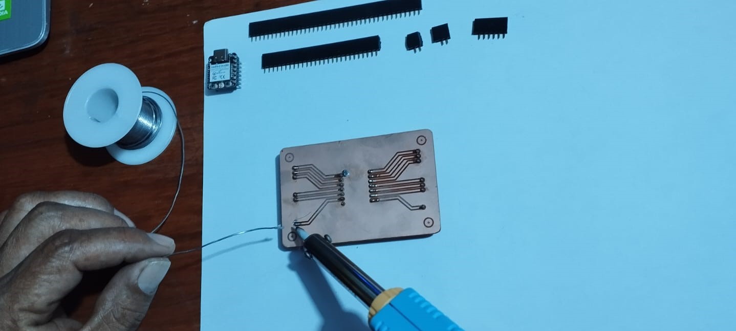
Soldering pin header
In this process we are soldering the pin header where the microcontroller will go.
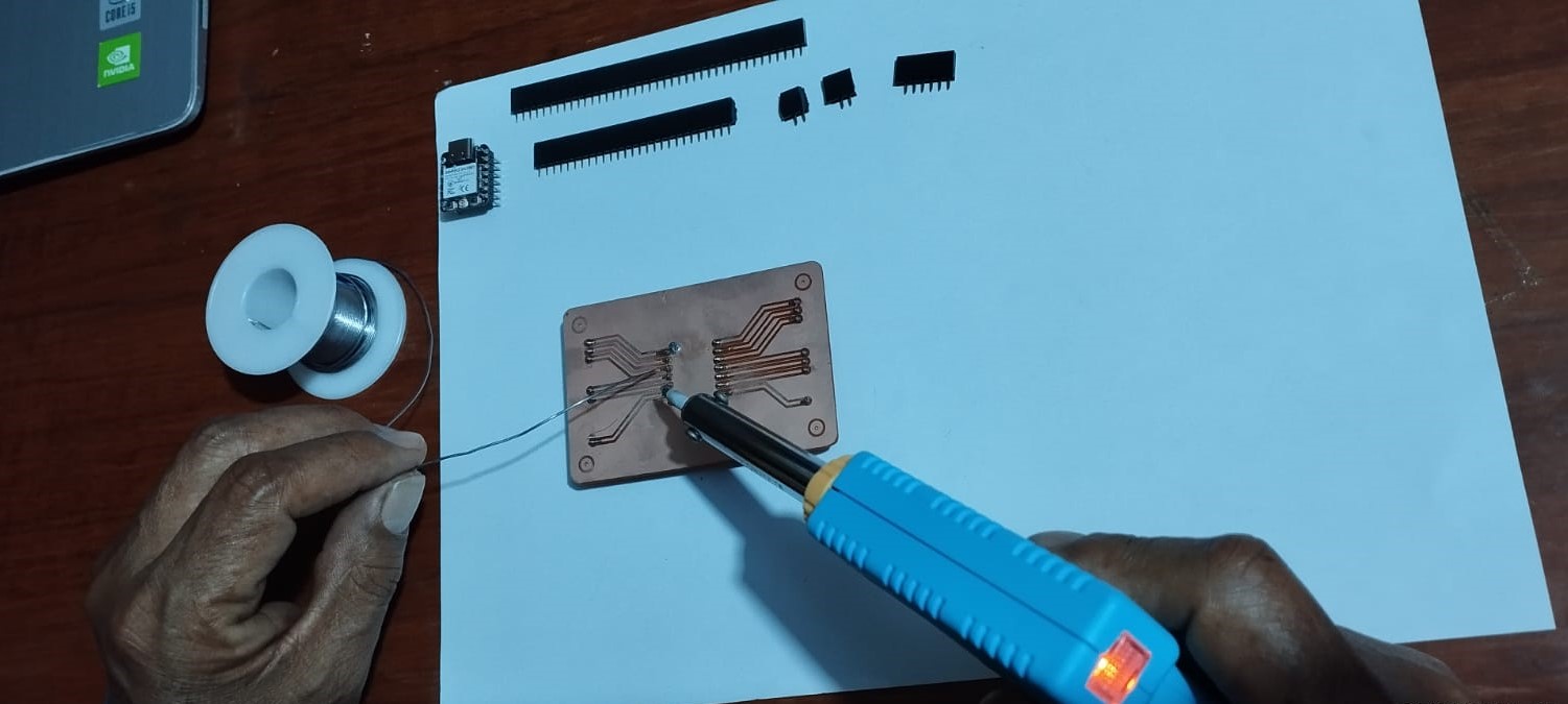
Soldering pin header
To solder the through-pin headers, we must place the tip of the soldering iron in contact with the component pin, then the copper pad, then wait 1 to 2 seconds for both to reach temperature.
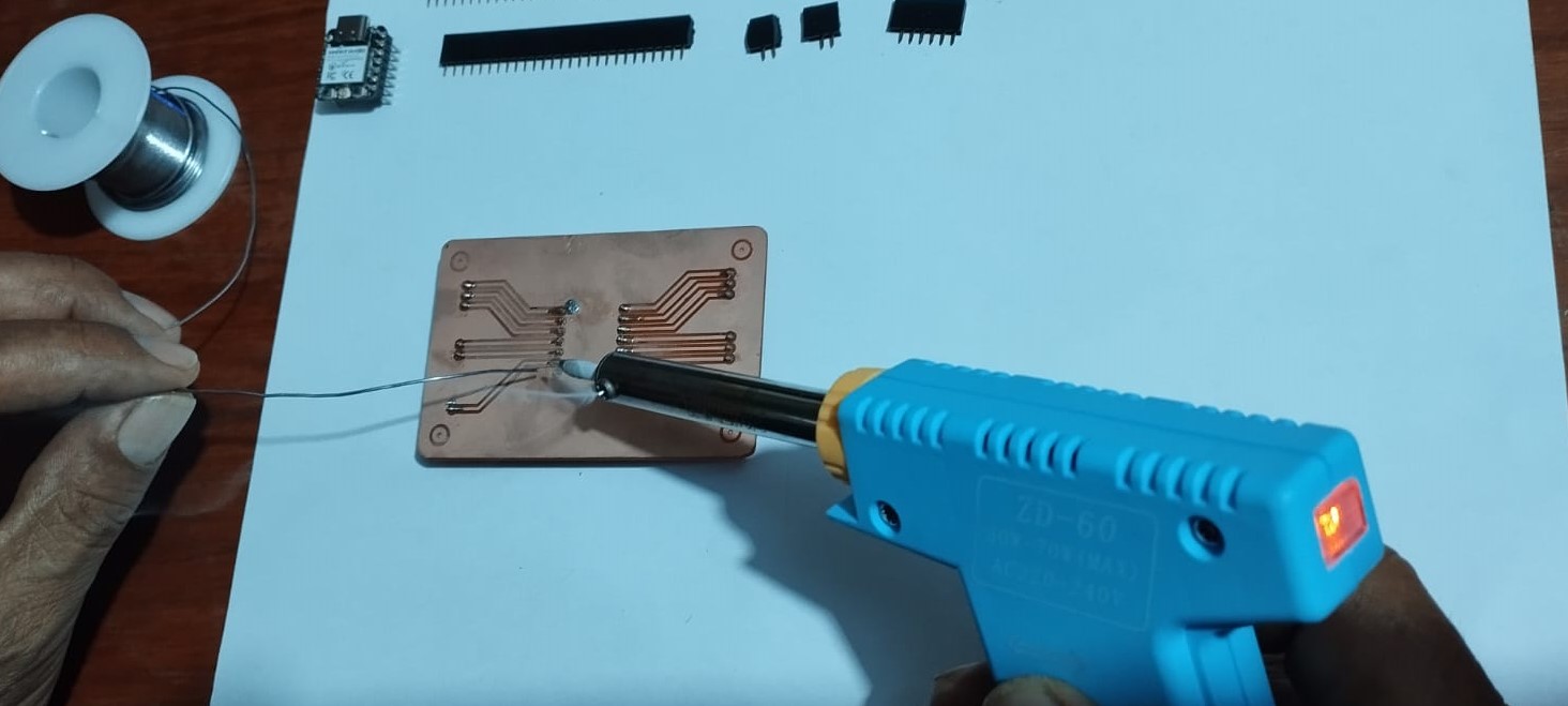
Through-hole soldering
We proceed to solder the other end of the tracks, where the two and three pin headers will go.
In this way, all the components are finished soldering, in this case all the through-pin headers, trying to ensure that the soldering is done correctly.
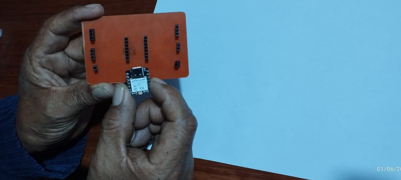
Placing the microcontroller
Once we have finished soldering all the through pin headers, we place the microcontroller in its position.
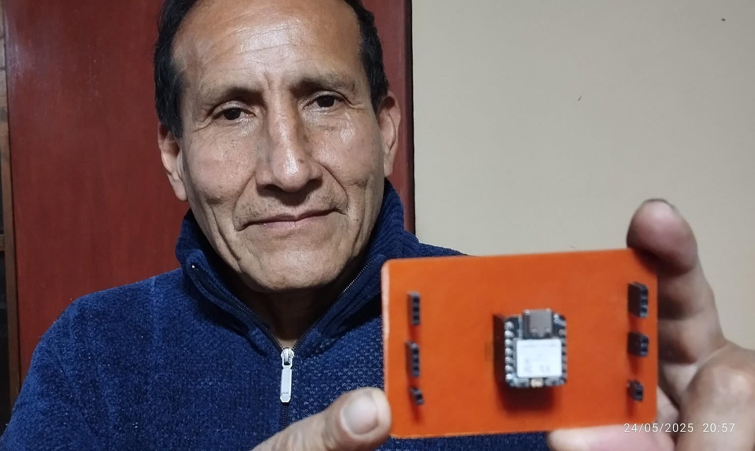
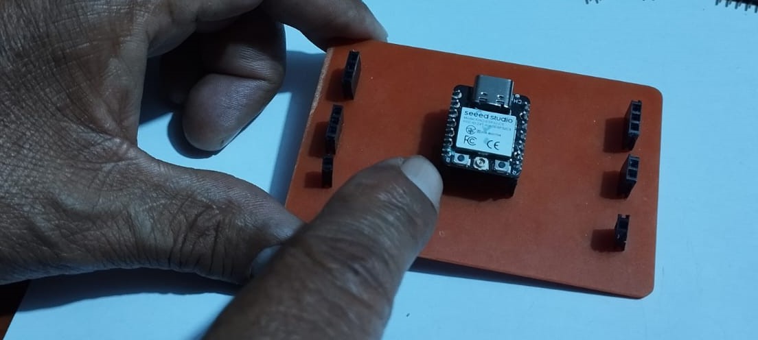
Microcontroller inside the PCB
The microcontroller has snapped into place, and the PCB is now ready for testing.
View of the weld on the bottom layer
You can see that the welding is fine, just as we expected, there is no short circuit.
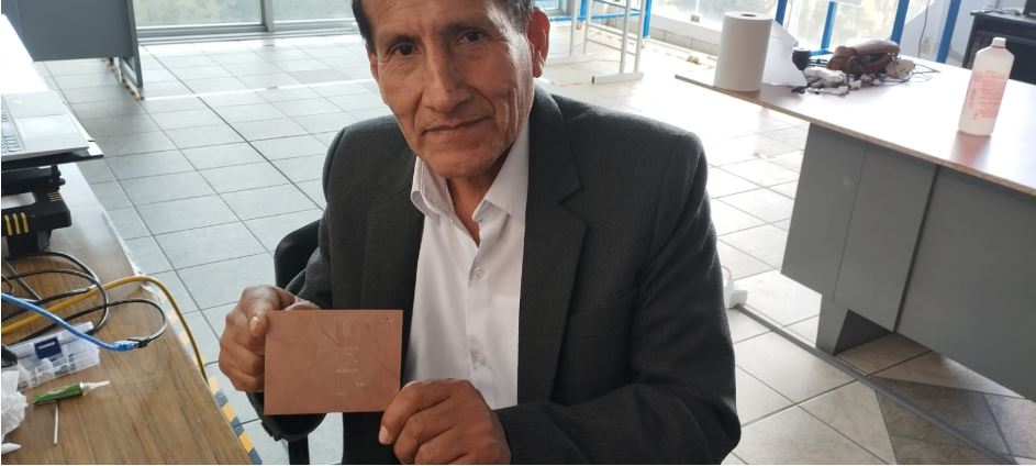
Finished PCB
The components were properly soldered, ensuring good electrical contact. The board was ready for testing and integration with the rest of the system.
Test a microcontroller development board
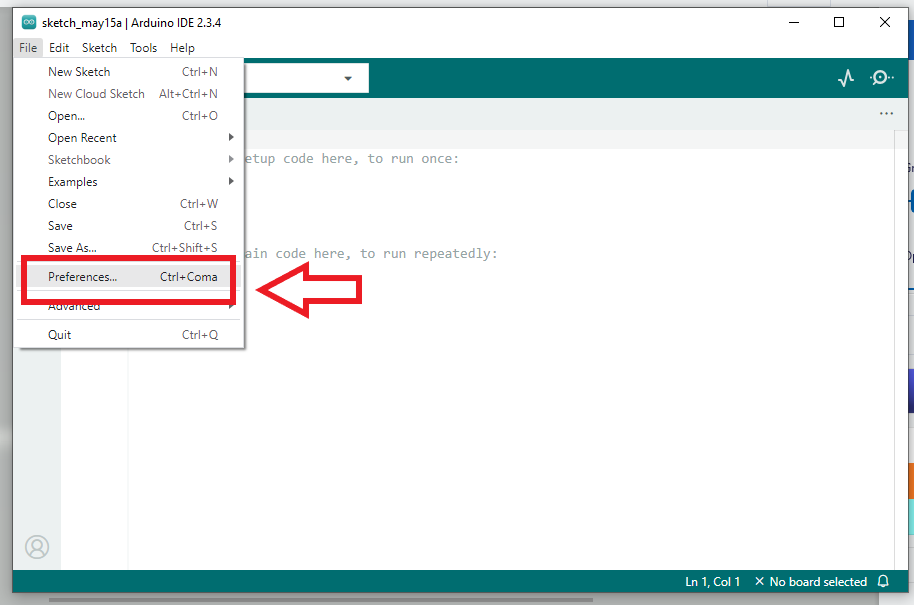
To test our microcontroller development board, we will do so using the Arduino IDE. To do this, we download it from its main page. Once installed, we will follow these steps:
Step 1: Install ESP32 Board Support
Open the Arduino IDE.
Go to File > Preferences.
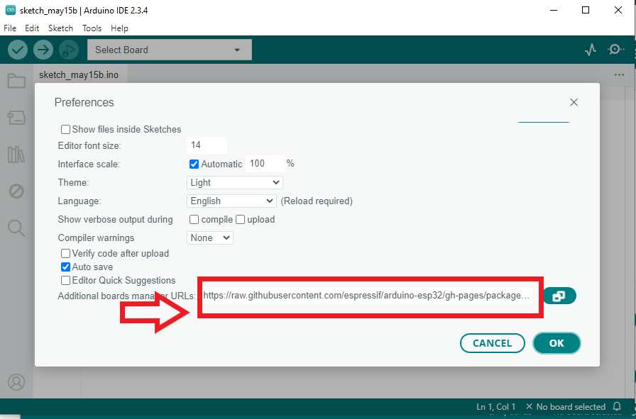
In the "Additional Board Manager URLs" field, add the following URL:
https://raw.githubusercontent.com/espressif/arduino-esp32/gh-pages/package_esp32_index.json
Click "OK" to save.
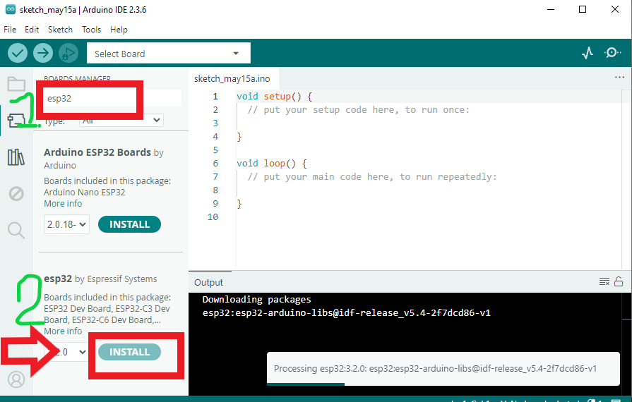
Go to Tools > Board > Boards Manager.
Search for esp32.
Click "Install" on the package named esp32 by Espressif Systems.
Step 2: Select the Correct Board
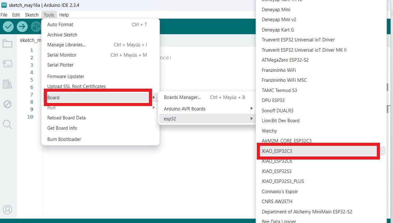
Go to Tools > Board.
Select ESP32C3 Dev Module or Seeed XIAO ESP32C3 if available.
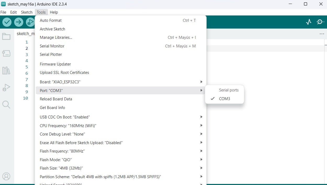
Go to Tools > Port and select the COM port assigned to your board.
If the port is not visible, press and hold the BOOT button on the board while uploading the sketch.
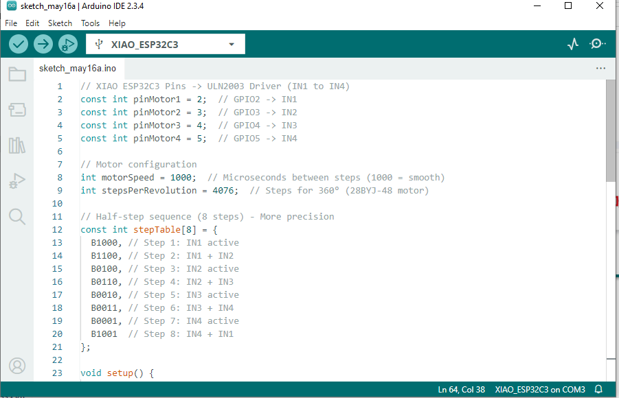
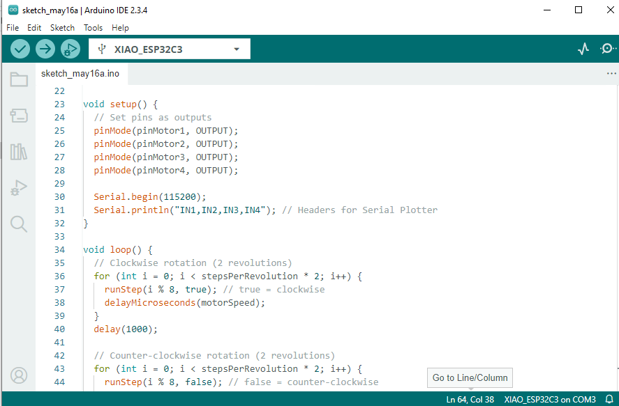
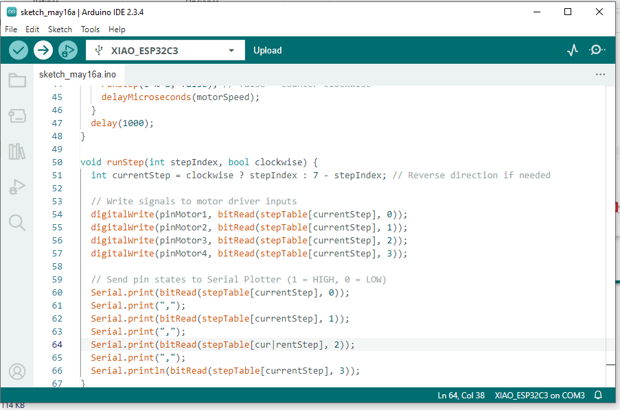
Control of a Stepper Motor
For the first test, as part of our project we are going to control a 28BYJ-48 stepper motor with a ULN2003 driver using our designed XIAO ESP32-C3 board, first we will load the code to the Arduino IDE, we connect our board to the COM3 port and compile, the code loaded correctly. The video shows the control of the stepper motor
Stepper motor demo in action
Conclusions
In conclusion, this project requires a lot of technical skills, in my experience I have previously had the opportunity to work in a microsoldering laboratory, which is why it was not so complicated to solder the components, but apart from that it requires a lot of patience to manufacture the PCB, it was the first time doing this job, which I really liked the way we can manufacture our own PCBs, which requires a lot of patience in every step of the process, satisfactory results can be achieved in the production of electronics using a CNC milling machine and the XIAO ESP32-C3 microcontroller.


.jpeg)
.jpeg)
.jpeg)
.jpeg)